EP1265361A2 - Complementary signal generation circuit - Google Patents
Complementary signal generation circuit Download PDFInfo
- Publication number
- EP1265361A2 EP1265361A2 EP02090206A EP02090206A EP1265361A2 EP 1265361 A2 EP1265361 A2 EP 1265361A2 EP 02090206 A EP02090206 A EP 02090206A EP 02090206 A EP02090206 A EP 02090206A EP 1265361 A2 EP1265361 A2 EP 1265361A2
- Authority
- EP
- European Patent Office
- Prior art keywords
- node
- signal
- drain
- gate
- effect transistor
- Prior art date
- Legal status (The legal status is an assumption and is not a legal conclusion. Google has not performed a legal analysis and makes no representation as to the accuracy of the status listed.)
- Withdrawn
Links
- 230000000295 complement effect Effects 0.000 title claims abstract description 68
- 230000007274 generation of a signal involved in cell-cell signaling Effects 0.000 title claims abstract description 52
- 238000012546 transfer Methods 0.000 claims description 56
- 239000003990 capacitor Substances 0.000 claims description 19
- 230000005669 field effect Effects 0.000 claims 49
- 238000004519 manufacturing process Methods 0.000 abstract description 30
- 230000008859 change Effects 0.000 abstract description 22
- 230000003111 delayed effect Effects 0.000 abstract description 12
- 230000001934 delay Effects 0.000 abstract description 4
- 238000010586 diagram Methods 0.000 description 21
- 230000000694 effects Effects 0.000 description 10
- 238000004088 simulation Methods 0.000 description 6
- 238000012423 maintenance Methods 0.000 description 3
- 238000000034 method Methods 0.000 description 3
- 230000009467 reduction Effects 0.000 description 3
- ATJFFYVFTNAWJD-UHFFFAOYSA-N Tin Chemical compound [Sn] ATJFFYVFTNAWJD-UHFFFAOYSA-N 0.000 description 2
- 238000013461 design Methods 0.000 description 2
- 238000005259 measurement Methods 0.000 description 2
- 230000003071 parasitic effect Effects 0.000 description 2
- 230000008054 signal transmission Effects 0.000 description 2
- 235000013599 spices Nutrition 0.000 description 2
- 230000004075 alteration Effects 0.000 description 1
- 230000003321 amplification Effects 0.000 description 1
- 230000005540 biological transmission Effects 0.000 description 1
- 238000012938 design process Methods 0.000 description 1
- RGNPBRKPHBKNKX-UHFFFAOYSA-N hexaflumuron Chemical compound C1=C(Cl)C(OC(F)(F)C(F)F)=C(Cl)C=C1NC(=O)NC(=O)C1=C(F)C=CC=C1F RGNPBRKPHBKNKX-UHFFFAOYSA-N 0.000 description 1
- 230000003993 interaction Effects 0.000 description 1
- 230000001788 irregular Effects 0.000 description 1
- 238000012986 modification Methods 0.000 description 1
- 230000004048 modification Effects 0.000 description 1
- 238000003199 nucleic acid amplification method Methods 0.000 description 1
- 230000004044 response Effects 0.000 description 1
- 230000011664 signaling Effects 0.000 description 1
Images



Classifications
-
- H—ELECTRICITY
- H03—ELECTRONIC CIRCUITRY
- H03K—PULSE TECHNIQUE
- H03K3/00—Circuits for generating electric pulses; Monostable, bistable or multistable circuits
- H03K3/01—Details
- H03K3/011—Modifications of generator to compensate for variations in physical values, e.g. voltage, temperature
-
- H—ELECTRICITY
- H03—ELECTRONIC CIRCUITRY
- H03K—PULSE TECHNIQUE
- H03K3/00—Circuits for generating electric pulses; Monostable, bistable or multistable circuits
- H03K3/02—Generators characterised by the type of circuit or by the means used for producing pulses
- H03K3/353—Generators characterised by the type of circuit or by the means used for producing pulses by the use, as active elements, of field-effect transistors with internal or external positive feedback
- H03K3/356—Bistable circuits
- H03K3/356104—Bistable circuits using complementary field-effect transistors
- H03K3/356113—Bistable circuits using complementary field-effect transistors using additional transistors in the input circuit
Definitions
- the present invention relates to a complementary signal generation circuit, and relates in particular to a complementary signal generation circuit for receiving a signal and for generating, for the input signal, a complementary signal that includes an in-phase signal and an antiphase signal.
- LVDS Low-Voltage Differential Signaling
- a fast signal transmission/reception circuit is a technique employed for transferring data using a complementary signal that includes an in-phase signal and an antiphase signal having a small amplitude of about 0.4 V.
- LVDS is characterized by providing excellent noise resistance, low power consumption and high-speed operation; however, LVDS also has two problems. The first problem is waveform distortion caused by jitter, and the second problem is waveform distortion due to fluctuation of a transistor characteristic, such as a threshold voltage, that is caused by the primary manufacturing factor.
- the jitter since with LVDS complementary signals are transmitted along a pair of signal lines, not only does jitter occur in a reception circuit, but also the jitter may cause the phase of a complementary input signal to shift in the opposite direction, so that it is difficult for an output signal cross point, a term used to designate a point whereat an in-phase signal and an antiphase signal intersect, to be located and maintained near a position representing 50% of the amplitude of the signals.
- eye pattern standards are specified for a fast interface, such as SONET/SDH, InfiniBand or FiberChannel, and cross point locations are set so they are near locations representing 50% of the amplitude of signals.
- An eye pattern method is employed to observe a target signal by superimposing an eye pattern on a clock cycle. Using this method, it is possible to efficiently observe the waveform distortion of an input signal and the fluctuation of an output waveform that are caused, for example, by jitter or a signal delay that occurs as the result of amplification.
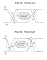
- FIG. 1A is a diagram showing the fluctuation of an output waveform due to jitter and a shaded area, defined by the eye pattern standards, that the waveform should not overlap. If a cross point can-not be maintained at a location near the 50% point of the amplitude of the signals, the eye pattern will be distorted and the standards will not be satisfied.
- the second problem is that, as is shown in FIG. 1B, the inclination of the leading/falling edge of an output signal fluctuates due to the characteristic change that is caused by a primary manufacturing factor. Since the fluctuation of the inclination due to the characteristic change that is caused by the manufacturing factor is large, and the fluctuation direction may differ for both complementary signals, cross points may be generated at various positions, such as P91 to P95, or no cross point may be generated, so that a satisfactory margin relative to the eye pattern standards can not be obtained.
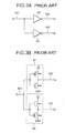
- FIG. 2 is a circuit diagram showing a first conventional complementary signal generation circuit. An input signal 101 is passed through inverters 15 and 16, and is output as an in-phase signal 103, and is also passed through the inverters 15, 16 and 17, and is output as an antiphase signal 102.
- the effect produced by the jitter and the distortion of the eye pattern is smaller than that for the LVDS.
- the number of inverter stages from the input to the in-phase output differs from the number of inverter stages from the input to the anti-phase output, i.e., in the first case it is two and in the second it is three.
- the output waveform fluctuates due to the characteristic change caused by the manufacturing factor, and distortion of the eye pattern occurs.
- the sum of the delay of the inverter 17 and the delay produced by the inverter 18 must be substantially equal to the delay produced by the inverter 16, so that the inclination of the change of the in-phase signal 103 must be much greater than the inclination of the change of the antiphase signal 102. Accordingly, the change in the inclination of the in-phase signal 103 accompanied by the characteristic variance of the transistor would be increased.
- FIGs. 3A and 3B are circuit diagrams showing a complementary signal generation circuit disclosed in Japanese Patent Laid-Open No. 03-258015.
- an inverter 81 and a buffer circuit 82 constitute a complementary signal generation circuit, and a signal 101 is input to the inverter 81 and the buffer circuit 82.
- the inverter 81 inverts the input signal 101, and generates an antiphase signal 102, while the buffer circuit 82 uses the input signal 101 to generate an in-phase signal 103.
- the inverter 81 is so designed that a p channel MOS transistor Qp21 and an n channel MOS transistor Qn21 are connected in series between a power source and the ground
- the buffer circuit 82 is so designed that an n channel MOS transistor Qn22 and a p channel MOS transistor Qp22 are connected in series between a power source and the ground.
- the absolute value of the gain of the inverter 81 is large near the point representing 50% of the amplitude, while the absolute value of the gain of the buffer circuit 82 is small, the response to a change in the input signal 102 differs between the inverter 81 and the buffer circuit 82. Therefore, in the second conventional complementary signal generation circuit, when a transistor characteristic, such as a threshold voltage, is changed due to a manufacturing factor, the delay and the inclination of the waveform vary for each complementary signal, and it is difficult to adjust a cross point so as to satisfy the eye pattern standards.
- a transistor characteristic such as a threshold voltage
- a complementary signal generation circuit comprises:
- the capacitor of the first RC series circuit may be constituted by a P channel MOS transistor, the source and the drain of which are connected to the first power source and the gate of which is connected to the first node
- the capacitor of the second RC series circuit may be constituted by a P channel MOS transistor, the source and the drain of which are connected to the first power source and the gate of which is connected to the third node.
- the first transfer gate of the first RC series circuit may include:
- the complementary signal generation circuit of the basic configuration may further comprise:
- the complementary signal generation circuit of the basic configuration may further comprise:
- both the source of the first P channel MOS transistor and the source of the second P channel MOS transistor may be connected to a third power source for supplying a higher voltage than the fist power source.
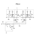
- the complementary signal generation circuit of FIG. 4 comprises: a flip-flop 1, a first RC series circuit 2, a second RC series circuit 3, and a complementary signal generator 6.
- This complementary signal generation circuit receives a signal 101, and outputs externally an antiphase signal 102 and a in-phase signal 103.
- the complementary signal generator 6 includes inverters 11 and 12.
- the inverter 11 receives input signal 101, and outputs a first internal signal 104 having a phase opposite to that of input signal 101, and inverter 12 receives the first internal signal 104 and outputs a second internal signal 105 having the same phase as input signal 101.
- the flip-flop 1 includes: a transistor Qp1, which is a first p channel MOS transistor; a transistor Qp2, which is a second p channel MOS transistor; a transistor Qn1, which is a first n channel MOS transistor; and a transistor Qn2, which is a second n channel MOS transistor.
- the first RC series circuit 2 includes: a transistor Qp3, which is a third p channel MOS transistor; and a transfer gate G1, which is a first transfer gate.
- the second RC series circuit 3 includes a transistor Qp4. which is a p channel MOS transistor; and a transfer gate G2, which is a second transfer gate.
- the capacitance between their gates and the channels is used as a capacitance element, and for transfer gate G1 and transfer gate G2, the ON resistance is used as a resistance element.
- the source and the drain of transistor Qp3 are connected to a power source VDD, which is a first power source, to which the source and drain of transistor Qp4 are also connected.
- the transfer gate G1 includes an n channel MOS transistor and a p channel MOS transistor. The sources of these transistors are connected and are also connected in common to the gate of transistor Qp3, the drains thereof are connected and are also connected in common to the gate of transistor Qn1 in flip-flop 1.
- the gate of the n channel MOS transistor is connected to the power source VDD, and the gate of the p channel MOS transistor is connected to a ground level that is a second power source.
- the transfer gate G2 includes an n channel MOS transistor and a p channel MOS transistor, the sources of which are connected and are also connected in common to the gate of transistor Qp4, and the drains of which are connected and are also connected in common to the gate of transistor Qn2 in flip-flop 1.
- the gate of the n channel MOS transistor is connected to power source VDD, and the gate of the p channel MOS transistor is grounded.
- the gate of transistor Qp4 is connected via transfer gate G2 to the gate of transistor Qn2 and the output terminal of inverter 12
- the gate of transistor Qp3 is connected via transfer gate G1 to the gate of transistor Qn1, the output terminal of inverter 11 and the input terminal of inverter 12.
- the source of transistor Qp1 and the source of transistor Qp2 are connected to power source VDD, while the gate of transistor Qp1 is connected to the drains of transistors Qp2 and Qn2 and the gate of transistor Qp2 is connected to the drains of transistors Qp1 and Qn1.
- the sources of both transistor Qn1 and transistor Qn2 are grounded.
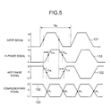
- H along the vertical axis represents a high level
- Y indicates an intermediate level
- L indicates a low level
- the intermediate level (Y level) is the level at 50% of the amplitude calculated from the low level (L) and the high level (H level).
- the input signal 101 is a signal whereby a change in level H or level L is repeated at cycle Tin, and is transmitted to the input terminal of inverter 11.
- the inverter 11 inverts input signal 101 and outputs a first internal signal 104 to the gate of the transistor Qn1, which is one of the input terminals for flip-flop 1, to the input terminal of inverter 12 and to transfer gate G1 of first RC series circuit 2.
- the inverter 12 generates a second internal signal 105 by inverting the first internal signal 104, and transmits second internal signal 105 to the gate of transistor Qn2, which is the other input terminal of flip-flop 1, and to transfer gate G2 of second RC series circuit 3.
- the second internal signal 105 is delayed more than the first internal signal 104 by a time equivalent to the length of the distance required for the transmission via inverter 12.
- the flip-flop 1 has two holding states in which either the transistor Qp1 or the transistor Qp2 is maintained ON.
- the determination of the holding state is dependant on which of the internal signals, the first internal signal 104 or the second internal signal 105, goes to level H.
- the first internal signal 104 and the second internal signal 105 alternately go to level H at cycle Tin.
- the flip-flop Based on the holding state that is determined, the flip-flop outputs the in-phase signal 103 from the drain of transistor Qn1, which is one of the output terminals, and outputs antiphase signal 102 from the drain of transistor Qn2, which is the other output terminal.
- the first RC series circuit 2 is equivalent to a circuit wherein a resistor and a capacitor are connected in series.
- the transfer gate G1 is always in the ON state, and this ON-resistance of transfer gate G1 serves as resistance element of the series circuit, while the capacitance between the gate and the channel of transistor Qp3 serves as capacitance of the series circuit.
- the first RC series circuit 2 is connected between the gate of transistor Qn1 and power source VDD, and acts as an effective load on inverter 11.
- second RC series circuit 3 acts as an effective load on inverter 12.
- the level change of input signal 101 is transmitted as a level inversion operation performed by the logical elements along the signal path, and the levels of antiphase signal 102 and in-phase signal 103 are changed.
- the logical elements along the signal path indicate inverters 11 and 12 and transistors Qn1, Qn2, Qp1 and Qp2.
- the number of logical stages which represents the number of level inversion operations performed by the logical elements, is different.
- in-phase signal 103 rises through the level inversion operation performed by transistor Qp1.
- the input signal 101 is transmitted along signal path L2 consisting of four logical stages for which the level inversion operation of transistor Qp1 is added to signal path L1. Since the number of logical stages along signal path L2 is greater by one than that for the signal path L1, the rise start time of in-phase signal 103 is delayed from the fall start time of antiphase signal 102.
- the transistor Qp1 is so designed that its ON resistance is smaller than that for transistor Qn2, and the inclination of the waveform is greater for the rise of in-phase signal 103 than for the fall of antiphase signal 102.
- a delay time THL from the time at which input signal 101 rises and goes to level Y to the time at which antiphase signal 102 falls and goes to level Y, and delay time THH, the period before in-phase signal 103 rises and goes to level Y, are measured by using circuit simulation. Based on measurement results, transistors Qp1 and Qn2 are designed so that the timings for them correspond to delay times THL and THH. Thus, antiphase signal 102 and in-phase signal 103 go to level Y at the same time and pass through cross points p1 and p3.
- antiphase signal 102 rises as a result of the level inversion operation performed by transistor Qp2.
- the input signal 101 is transmitted along a signal path L4 consisting of three logical stages and formed by adding the level inversion operation of transistor Qp2 to signal path L3. Since the number of stages along signal path L4 is larger by one than along signal path L3, for antiphase signal 102 the rise start time is delayed more than is the fall start time for in-phase signal 103.
- transistor Qp2 Since transistor Qp2 is so designed that its ON resistance is smaller than of transistor Qn1, the inclination of the waveform when antiphase signal 102 rises is larger than when in-phase signal 103 falls.
- a TLH delay time, from the time the input signal 101 falls and goes to level L to the time antiphase signal 102 rises and goes to level Y, and the delay time TLL, the period before in-phase signal 103 falls and goes to level Y, are measured by using a circuit simulation. Based on the measurement results, transistors Qp2 and Qn1 are designed so that the time for them correspond to delay times TLH and TLL. Thus, antiphase signal 102 and in-phase signal 103 go to level Y at the same time and pass through cross points p2 and p4.
- FIG. 6 is a diagram showing the function of the circuit in FIG. 4.
- the solid lines indicate original antiphase signal 102 and original in-phase signal 103, and P11 and P13 denote original cross points not affected by jitter.
- P11 and P13 denote original cross points not affected by jitter.
- Jitter occurring in the circuit is a phenomenon whereby, when multiple signal paths differ, irregular fluctuation is generated during the signal delay period by an effect produced by a parasitic element.
- antiphase signal 102 When the rise of input signal 101 is delayed by jitter, antiphase signal 102 is delayed along signal path L1, and in-phase signal 103 is delayed along signal path L2. Since almost all of signal path L2 is common to signal path L1, the delay time for antiphase signal 102 is substantially equal to the delay time for in-phase signal 103.
- delay times THL and THH are increased in the same manner. Since the increase in delay between the fall of antiphase signal 102 and the rise of in-phase signal 103 is substantially equal, the two signals are shifted from the solid lines to the broken lines, in parallel to the time axis. And since cross point P11 is shifted to cross point P12, in parallel to the time axis, cross point P12 as well as cross point P11 is maintained at level Y.
- in-phase signal 103 is delayed along signal path L3, and antiphase signal 102 is delayed along signal path L4. Since almost the entire signal path L4 is common to signal path L3, the delay time for in-phase signal 103 is substantially equal to the delay time for antiphase signal 102.
- delay times TLL and TLH are increased in the same manner. Since the increase in delay is substantially equal between the fall of in-phase signal 103 and the rise of antiphase signal 102, the two signals are shifted from the solid lines to the broken lines, in parallel to the time axis. And since cross point P13 is moved to cross point P14, in parallel to the time axis, cross point P14 as well as cross point P13 is maintained at level Y.
- FIG. 7 is a diagram showing the function of the circuit of FIG. 4.
- the ON resistance of the n channel MOS transistor is changed by the characteristic change due to the manufacturing factor, e.g., depending on whether a longer or shorter channel is prepared for the MOS transistor, whether a higher or lower threshold value is obtained, and whether a gate insulating film is formed thicker or thinner. Then, the inclination of the complementary signal is changed.
- the cross point P21 at the intersection of antiphase signal 102 and in-phase signal 103 which are indicated by solid lines, represents the time when no affect is produced by the manufacturing factor.
- the cross points P22 and P23 at antiphase signal 102 and in-phase signal 103 represented by broken lines, indicate when an affect is produced by the manufacturing factor. For the rise of input signal 101, the inclination of falling antiphase signal 102 and the rise of in-phase signal 103 change due to the manufacturing factor.
- the ON resistance of the n channel MOS transistor is reduced due to the manufacturing factor, e.g., when the threshold voltage of the n channel MOS transistor is reduced and is lower than usual, the ON resistance of transistor Qn2 is reduced and the driving capability is increased, so that the inclination of the fall of antiphase signal 102 is increased.
- the threshold voltage of the n channel MOS transistor of transfer gate G2 is also reduced, so that the ON resistance of transfer gate G2 is reduced.
- the resistance of second RC series circuit 3 is reduced, and acts as an increase in the effective load on inverter 12.
- the ON resistance of the n channel MOS transistor is increased due to the effect of a manufacturing factor, e.g., when the threshold voltage of the n channel MOS transistor is set higher than normal, the ON resistance of transistor Qn2 is increased and the driving capability is reduced, so that the inclination of the fall of antiphase signal 102 is reduced.
- the threshold voltage of the n channel MOS transistor of transfer gate G2 is also increased, the ON resistance of transfer gate G2 is increased.
- the ON resistance of second RC series circuit 3 is increased and this reduces the effective load on inverter 12.
- the inclinations of the fall of in-phase signal 103 and the rise of antiphase signal 102 are changed due to the manufacturing factor.
- the first RC series circuit 2 as well as the second series circuit 3 acts as an effective load on inverter 11 relative to the affect of the manufacturing factor.
- the change in the inclinations of in-phase signal 103 and antiphase signal 102 are suppressed and the cross point is maintained at level Y.
- Transfer gates G1 and G2 each include an n channel and a p channel MOS transistor.
- the p channel MOS transistor may be deleted from transfer gate G1 in FIG. 4, and transfer gate G1 may be constituted only by an n channel MOS transistor, the gate of which is connected to power source VDD.
- the p channel MOS transistor may be deleted from transfer gate G2 in FIG. 4, and transfer gate G2 may be constituted only by an n channel MOS transistor, the gate of which is connected to power source VDD.
- FIG. 8 is a diagram showing the results obtained when a simulation was performed using a circuit simulator SPICE for the example in FIG. 2 and the circuit in FIG. 4. Delay times THH and TLL for in-phase signal 103 were measured.
- the circuit in FIG. 4 is operated, as is normal, under the design condition wherein the channel length, the threshold voltage and the thickness of the gate insulating film are standard values, and under an operating condition wherein the power voltage is 1.8 V and the temperature is 25°C.
- the SLOW condition and the FAST condition are assumed as conditions for the affect produced by a manufacturing factor.
- the simulation is performed by using a characteristic parameter obtained when the channel length is greater than the standard value, the absolute value of the threshold voltage is high and the thick gate insulating film is formed, and by setting a power voltage of 1.65 V and a temperature of 125°C. Further, under the FAST condition, the simulation is performed by using a characteristic parameter obtained when the channel length is shorter than the standard value, the absolute value of the threshold voltage is low and the thin gate insulating film is formed, and by setting the power voltage of 1.95 V and temperature of -40°C.
- the variance value is a difference between the results obtained under SLOW condition and the results obtained under FAST condition.
- delay time THH is reduced from 0.713 to 0.0666, and delay time TLL is reduced form 0.0943 to 0.0768, so that the cross point maintenance function is effectively performed.
- the embodiment almost all the portions of the signal paths for in-phase signal 103 and antiphase signal 102 are formed by using the same paths of complementary signal generator 6 and flip-flop 1. Therefore, since the changes in the delays due to jitter occur in the same direction, the effect of jitter on cross point change can be suppressed and the cross point can be maintained so it is near 50% of the amplitude. Further, according to the embodiment, since the ON resistances of transistors Qn1 and Qn2 are changed, RC series circuits act to suppress the fluctuations in the driving capacities of transistors Qn1 and Qn2. Thus, the affect of the manufacturing factor on the shifting of the cross point can be suppressed, and the cross point can be maintained near 50% of the amplitude.
- FIG. 9 is a circuit diagram showing a second embodiment of the invention. RC series circuits 4 and 5 are added to the circuit in FIG. 4, so that the cross point maintenance function is performed even when the ON resistance of the p channel MOS transistor is changed due to the affect of a manufacturing factor.
- RC series circuit 4 includes an n channel MOS transistor Qn3 and a transfer gate G3
- RC series circuit 5 includes n channel MOS transistor Qn4 and transfer gate G4.
- the capacitance between the gate and the channel serves as capacitance element
- the transfer gates G3 and G4 the ON resistance serves as resistance element.
- Transfer gate G3 includes paired n channel and p channel MOS transistors. The sources of these transistors are connected and are also connected in common to the gate of transistor Qn3, the drains are connected and are also connected in common to the drain of transistor Qn2 in flip-flop 1, and the gate of the p channel MOS transistor is grounded.
- Transfer gate G4 includes paired n channel and p channel MOS transistors. The sources of these transistors are connected and are also connected in common to the gate of transistor Qn4, the drains are connected and are also connected in common to the drain of transistor Qn1 in flip-flop 1. The gate of the n MOS transistor is connected to power source VDD, and the gate of the p channel MOS transistor is grounded.
- the gate of transistor Qn4 is connected via transfer gate G4 to the drain of transistor Qp1
- the gate of transistor Qn3 is connected via transfer gate G3 to the drain of transistor Qp2.
- the ON resistance of the p channel MOS transistor is reduced by the effect produced by the manufacturing factor, e.g., when a small absolute value for the threshold voltage of the p channel MOS transistor is obtained during the manufacturing process, the driving capacities of transistors Qp1 and Qp2 increase , so that the potential of the drain sharply increases.
- the ON resistance of the p channel MOS transistor increases by the effect produced by the manufacturing factor, e.g., when absolute value for the threshold voltage of the p channel MOS transistor is higher than usual, the driving capacities of transistors Qp1 and Qp2 are reduced, so that the inclination of the rise is reduced.
- RC series circuits 4 and 5 also act as effective loads to reduce the change in the inclination of the signal that is caused by a manufacturing factor of the p channel MOS transistor.
- the cross point can more effectively be maintained at level Y than in the first embodiment in FIG. 4.
- Transfer gates G3 and G4 have been constituted by an n channel MOS transistor and a p channel MOS transistor.
- the n channel MOS transistor may be deleted form transfer gate G3 in FIG. 9, and transfer gate G3 may be constituted only by the p channel MOS transistor, the gate of which is grounded.
- the n channel MOS transistor may be deleted from transfer gate G4 in FIG. 9, and transfer gate G4 may be constituted only by the p channel MOS transistor, the gate of which is grounded.
- FIG. 10 is a circuit diagram of a third embodiment, in which the complementary signal generation circuit is the same as in FIG. 4, except that an inverter 13, which is a first inverter, and an inverter 14, which is a second inverter, are included. Therefore, the FIG. 10 complementary signal generation circuit as well as that in FIG. 4, includes a function for maintaining a cross point by countering the effects of jitter and manufacturing factor.
- inverter 13 The input terminal of inverter 13 is connected to the drain of transistor Qn1, and antiphase signal 102 is output. While the input terminal of inverter 14 is connected to the drain of transistor Qn2, and in-phase signal 103 is output.
- the inverters 13 and 14 are constituted by CMOS circuits, and the ratio of the ON resistances of the n channel MOS transistor and the p channel MOS transistor is adjusted, so that the cross point of antiphase signal 102 and in-phase signal 103 is almost at 50% of the signal amplitude.
- the cross point of antiphase signal 102 and in-phase signal 103 can be adjusted by inverters 13 and 14 so it is at 50% of the signal amplitude. Therefore, strict adjustment of the cross point is not required for the design of the flip-flop, and the design process can be simplified.
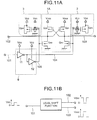
- FIG. 11A shows a circuit according to a fourth embodiment of the invention.
- the complementary signal generation circuit has a level shift function for receiving an input signal 101 having the voltage amplitude for a power source VDD, and for outputting an in-phase signal 103 and an antiphase signal 102 having the voltage amplitude of a power source VDD2, which is a third power source provided to supply a voltage higher than supplied by the power source VDD.
- the complementary signal generation circuit in this embodiment includes a flip-flop 1A instead of flip-flop 1 in FIG. 4.
- a voltage higher than that supplied by power source VDD is applied to flip-flop 1A, and the sources of transistors Qp1 and Qp2 are connected to power source VDD2.
- the complementary signal generation circuit in this embodiment receives input signal 101 of the voltage amplitude of power source VDD, and employs the level shift function to output antiphase signal 102 and in-phase signal 103 of the voltage amplitude of power source VDD2.
- the complementary signal generation circuit is not limited to these embodiments, and the invention includes various alterations and modifications of the configurations of the embodiments.
- the invention when the invention is applied, almost all portions of the signal paths for the in-phase and antiphase signal can be formed by using the same complementary signal generator and flip-flop paths. Since delays due to jitter are changed in the same direction, the affect of jitter on the fluctuation of a cross point can be suppressed, and the cross point can be maintained at near 50% of the amplitude. Further, according to the invention, when the ON resistance of a transistor changes, the RC series circuit acts to suppress a change in the driving capabilities of the transistors that constitute the flip-flop. Therefore, the affect of a manufacturing factor on the change of a cross point can be suppressed, and the cross point can be maintained at near 50% of the amplitude. Since the complementary signal generation circuit in this invention has a cross point maintenance function, eye pattern standards can be satisfied even when jitter or a manufacturing factor effect is present.
Landscapes
- Logic Circuits (AREA)
- Manipulation Of Pulses (AREA)
Abstract
Disclosed is a complementary signal generation circuit
that can suppress the distortion of an eye pattern due to a
change in signal delay caused by jitter or a change in the
rise and fall of a signal caused by a manufacturing factor.
An inverter 11 inverts an input signal 101 and generates a
first internal signal 104, and an inverter 12 inverts the
first internal signal 104 and generates a second internal
signal 105. When the first internal signal 104 goes high,
a flip-flop 1 reduces the level of an in-phase signal 103
to low, and increases the level of an antiphase signal 102
to high. Thus, when the fall of the in-phase signal is
delayed, the flip-flop also delays the rise of the
antiphase signal and suppresses the distortion of the eye
pattern. And when the ON resistances of transistors Qn1
and Qn2 are changed due to a manufacturing factor, RC
series circuits 2 and 3 suppress the change in the driving
capability.
Description
- The present invention relates to a complementary signal generation circuit, and relates in particular to a complementary signal generation circuit for receiving a signal and for generating, for the input signal, a complementary signal that includes an in-phase signal and an antiphase signal.
- Recently, signal transfer speeds have been increased, and fast operations exceeding 1 GHz are required for an input/output buffer. LVDS (Low-Voltage Differential Signaling), known as a fast signal transmission/reception circuit, is a technique employed for transferring data using a complementary signal that includes an in-phase signal and an antiphase signal having a small amplitude of about 0.4 V. LVDS is characterized by providing excellent noise resistance, low power consumption and high-speed operation; however, LVDS also has two problems. The first problem is waveform distortion caused by jitter, and the second problem is waveform distortion due to
fluctuation of a transistor characteristic, such as a threshold voltage, that is caused by the primary manufacturing factor. - According to the first problem, since with LVDS complementary signals are transmitted along a pair of signal lines, not only does jitter occur in a reception circuit, but also the jitter may cause the phase of a complementary input signal to shift in the opposite direction, so that it is difficult for an output signal cross point, a term used to designate a point whereat an in-phase signal and an antiphase signal intersect, to be located and maintained near a position representing 50% of the amplitude of the signals.
- Generally, eye pattern standards are specified for a fast interface, such as SONET/SDH, InfiniBand or FiberChannel, and cross point locations are set so they are near locations representing 50% of the amplitude of signals. An eye pattern method is employed to observe a target signal by superimposing an eye pattern on a clock cycle. Using this method, it is possible to efficiently observe the waveform distortion of an input signal and the fluctuation of an output waveform that are caused, for example, by jitter or a signal delay that occurs as the result of amplification. FIG. 1A is a diagram showing the fluctuation of an output waveform due to jitter and a shaded area, defined by the eye pattern standards, that the waveform should not overlap. If a cross point can-not be maintained at a location near the 50% point of the amplitude of the signals, the eye pattern will be distorted and the standards will not be satisfied.
- As is shown in FIG. 1A, according to LVDS, signal transmission is delayed by the effect of jitter, and when the fluctuation direction differs for both complementary signals, a cross point P81 is moved to P82, and a cross point P83 is moved to P84. Since the cross points are greatly shifted from locations near the 50% point of the amplitude signals, the adjustment of the cross points is difficult.
- The second problem is that, as is shown in FIG. 1B, the inclination of the leading/falling edge of an output signal fluctuates due to the characteristic change that is caused by a primary manufacturing factor. Since the fluctuation of the inclination due to the characteristic change that is caused by the manufacturing factor is large, and the fluctuation direction may differ for both complementary signals, cross points may be generated at various positions, such as P91 to P95, or no cross point may be generated, so that a satisfactory margin relative to the eye pattern standards can not be obtained.
- Explanation has been given that a circuit, such as an LVDS circuit, for inputting a complementary signal and outputting a complementary signal is greatly affected by jitter. On the other hand, for a complementary signal generation circuit for receiving one signal and for generating and outputting an in-phase signal and an antiphase signal thereof, when jitter affects an input signal, both the output in-phase signal and the output antiphase signal are moved in the same direction. Thus, although jitter occurs in the complementary signal generation circuit due to the interaction between
inverters input signal 101 is passed throughinverters phase signal 103, and is also passed through theinverters antiphase signal 102. - In the complementary signal generation circuit in FIG. 2, the effect produced by the jitter and the distortion of the eye pattern is smaller than that for the LVDS. However, in the complementary signal generation circuit shown in FIG. 2, the number of inverter stages from the input to the in-phase output differs from the number of inverter stages from the input to the anti-phase output, i.e., in the first case it is two and in the second it is three. Thus, the output waveform fluctuates due to the characteristic change caused by the manufacturing factor, and distortion of the eye pattern occurs. In order to locate the cross point near the 50% point of the amplitude, the sum of the delay of the
inverter 17 and the delay produced by theinverter 18 must be substantially equal to the delay produced by theinverter 16, so that the inclination of the change of the in-phase signal 103 must be much greater than the inclination of the change of theantiphase signal 102. Accordingly, the change in the inclination of the in-phase signal 103 accompanied by the characteristic variance of the transistor would be increased. - As a second conventional example, there is a complementary signal generation circuit wherein the number of gate stages from the input to the antiphase output is equal to the number of gate stages from the input to the in-phase output. FIGs. 3A and 3B are circuit diagrams showing a complementary signal generation circuit disclosed in Japanese Patent Laid-Open No. 03-258015. As is shown in FIG. 3A, an
inverter 81 and abuffer circuit 82 constitute a complementary signal generation circuit, and asignal 101 is input to theinverter 81 and thebuffer circuit 82. Theinverter 81 inverts theinput signal 101, and generates anantiphase signal 102, while thebuffer circuit 82 uses theinput signal 101 to generate an in-phase signal 103. - As is shown in FIG. 3B, the
inverter 81 is so designed that a p channel MOS transistor Qp21 and an n channel MOS transistor Qn21 are connected in series between a power source and the ground, and thebuffer circuit 82 is so designed that an n channel MOS transistor Qn22 and a p channel MOS transistor Qp22 are connected in series between a power source and the ground. - In the complementary signal generation circuit in FIGs. 3A and 3B, since the
input signal 101 is transmitted along a signal path formed of a single logical stage provided by either theinverter 81 or thebuffer circuit 82, theoretically the delays produced along the signal path by these two components are equal, and the start time of the change point is the same for theantiphase signal 102 and the in-phase signal 103. - However, in actuality, since the absolute value of the gain of the
inverter 81 is large near the point representing 50% of the amplitude, while the absolute value of the gain of thebuffer circuit 82 is small, the response to a change in theinput signal 102 differs between theinverter 81 and thebuffer circuit 82. Therefore, in the second conventional complementary signal generation circuit, when a transistor characteristic, such as a threshold voltage, is changed due to a manufacturing factor, the delay and the inclination of the waveform vary for each complementary signal, and it is difficult to adjust a cross point so as to satisfy the eye pattern standards. - To resolve the above described shortcomings of the conventional examples, it is one objective of the invention to provide a complementary signal generation circuit that can reduce the occurrence of waveform distortion due to jitter, and also that due to fluctuation of a transistor characteristic caused by a manufacturing factor.
- To achieve this objective, according to one aspect of the invention, a complementary signal generation circuit comprises:
- a complementary signal generator for generating an antiphase signal from a input signal, input at a signal input terminal, and outputting the antiphase signal from a first internal signal terminal, and for generating an in-phase signal from the input signal and outputting the in-phase signal from a second internal signal terminal;
- a flip-flop, including
- a first P channel MOS transistor, the source of which is connected to a first power source,
- a second P channel transistor, the source of which is connected to the first power source,
- a first N channel MOS transistor, the source of which is connected to a second power source and the drain of which is connected to the drain of the first P channel MOS transistor and the gate of the second P channel MOS transistor, and
- a second N channel MOS transistor, the source of which is connected to the second power source and the drain of which is connected to the drain of the second P channel MOS transistor and the gate of the first P channel MOS transistor;
- a first RC series circuit including
- a first transfer gate including an N channel MOS transistor, the source of which is connected to a first node, the gate of which is connected to the first power source and the drain of which is connected to a second node, and
- a capacitor connected to the first node; a second RC series circuit including
- a second transfer gate including an N channel MOS transistor, the source of which is connected to a third node, the gate of which is connected to the first power source and the drain of which is connected to a fourth node, and
- a capacitor connected to the third node; an in-phase signal output terminal for outputting an in-phase signal to the outside; and
- an antiphase signal output terminal for outputting an antiphase signal to the outside,
- wherein the first internal signal terminal is connected to the gate of the first N channel MOS transistor and the second node, the second internal signal terminal is connected to the gate of the second N channel MOS transistor and the fourth node, the drain of the first N channel MOS transistor is connected to the in-phase output terminal, and the drain of the second N channel MOS transistor is connected to the antiphase signal output terminal. This is the basic configuration.
-
- According to another aspect of the invention, for the complementary signal generation circuit of this basic configuration, the capacitor of the first RC series circuit may be constituted by a P channel MOS transistor, the source and the drain of which are connected to the first power source and the gate of which is connected to the first node, and the capacitor of the second RC series circuit may be constituted by a P channel MOS transistor, the source and the drain of which are connected to the first power source and the gate of which is connected to the third node.
- According to an additional aspect of the invention, for the complementary signal generation circuit of the basic configuration, the first transfer gate of the first RC series circuit may include:
- an N channel MOS transistor, the source of which is connected to the first node, the gate of which is connected to the first power source and the drain of which is connected to the second node; and
- a P channel MOS transistor, the source of which is
connected to the first node, the gate of which is connected
to the second power source and the drain of which is
connected to the second node. The second transfer gate of
the second RC series circuit may include:
- an N channel MOS transistor, the source of which is connected to the third node, the gate of which is connected to the first power source and the drain of which is connected to the fourth node; and
- a P channel MOS transistor, the source of which is connected to the third node, the gate of which is connected to the second power source and the drain of which is connected to the fourth node.
-
- According to a further aspect of the invention, the complementary signal generation circuit of the basic configuration may further comprise:
- a third RC series circuit including
- a third transfer gate including a P channel MOS transistor, the source of which is connected to a fifth node, the gate of which is connected to the second power source and the drain of which is connected to a sixth node, and
- a capacitor connected to the fifth node, wherein the sixth node is connected to the drain of the second N MOS transistor; and
- a fourth RC series circuit including
- a fourth transfer gate including a P channel MOS transistor, the source of which is connected to a seventh node, the gate of which is connected to the second power source and the drain of which is connected to an eighth node, and
- a capacitor connected to the seventh node, wherein the eighth node is connected to the drain of the first N channel MOS transistor.
-
- According to a still further aspect of the invention, the complementary signal generation circuit of the basic configuration may further comprise:
- a first inverter, the input terminal of which is connected to the drain of the first N channel MOS transistor and the output of which is connected to the antiphase signal output terminal; and
- a second inverter, the input terminal of which is connected to the drain of the second N channel MOS transistor and the output terminal of which is connected to the in-phase signal output terminal.
-
- According to yet another aspect of the invention, for the complementary signal generation circuit of the basic configuration, both the source of the first P channel MOS transistor and the source of the second P channel MOS transistor may be connected to a third power source for supplying a higher voltage than the fist power source.
- The above objectives and features and other relevant objectives and features will become apparent in due course during the following description given while referring to the accompanying drawings, and innovative matters pointed out in claims.
-
- FIG. 1A is a diagram showing distortion of an eye pattern due to jitter;
- FIG. 1B is a diagram showing distortion of an eye pattern due to a manufacturing factor;
- FIG. 2 is a circuit diagram showing a first conventional complementary signal generation circuit;
- FIG. 3A is a circuit diagram showing the logical gate level of a second conventional complementary signal generation circuit;
- FIG. 3B is a circuit diagram showing the transistor level of the second conventional complementary signal generation circuit;
- FIG. 4 is a circuit diagram showing a complementary signal generation circuit according to a first embodiment of the invention;
- FIG. 5 is a timing chart showing the operation of the complementary signal generation circuit according to the FIG. 4 embodiment;
- FIG. 6 is a diagram showing the function of the complementary signal generation circuit according to the first embodiment for maintaining a cross point relative to jitter;
- FIG. 7 is a diagram showing the function of the complementary signal generation circuit according to the first embodiment for maintaining a cross point relative to a manufacturing factor;
- FIG. 8 is a diagram showing a comparison, obtained through a SPICE simulation, between the complementary signal generation circuit of the first embodiment and the first conventional example for a delay time up until an in-phase signal is output for an input signal;
- FIG. 9 is a circuit diagram showing a complementary
signal generation circuit according to a second embodiment
of the invention that differs from the first
embodiment in that
RC series circuits - FIG. 10 is a circuit diagram showing a complementary
signal generation circuit according to a third embodiment
of the invention that differs from the first
embodiment in that an
input signal 101 is shaped by aninverter 14 and an in-phase signal 103 is output, and theinput signal 101 is shaped by aninverter 13 and anantiphase signal 102 is output; - FIG. 11A is a circuit diagram showing a complementary signal generation circuit according to a fourth embodiment of the invention; and
- FIG. 11B is a diagram showing the level shift function of the complementary signal generation circuit according to the fourth embodiment for receiving a signal having an amplitude VDD and for outputting an in-phase signal and an antiphase signal having an amplitude VDD2.
-
- The preferred embodiments of the present invention will now be described in detail while referring to the accompanying drawings. The complementary signal generation circuit of FIG. 4 comprises: a flip-
flop 1, a firstRC series circuit 2, a secondRC series circuit 3, and acomplementary signal generator 6. This complementary signal generation circuit receives asignal 101, and outputs externally anantiphase signal 102 and a in-phase signal 103. - The
complementary signal generator 6 includesinverters inverter 11 receivesinput signal 101, and outputs a firstinternal signal 104 having a phase opposite to that ofinput signal 101, andinverter 12 receives the firstinternal signal 104 and outputs a secondinternal signal 105 having the same phase asinput signal 101. - The flip-
flop 1 includes: a transistor Qp1, which is a first p channel MOS transistor; a transistor Qp2, which is a second p channel MOS transistor; a transistor Qn1, which is a first n channel MOS transistor; and a transistor Qn2, which is a second n channel MOS transistor. - The first
RC series circuit 2 includes: a transistor Qp3, which is a third p channel MOS transistor; and a transfer gate G1, which is a first transfer gate. The secondRC series circuit 3 includes a transistor Qp4. which is a p channel MOS transistor; and a transfer gate G2, which is a second transfer gate. - For transistors Qp3 and Qp4, the capacitance between their gates and the channels is used as a capacitance element, and for transfer gate G1 and transfer gate G2, the ON resistance is used as a resistance element.
- The source and the drain of transistor Qp3 are connected to a power source VDD, which is a first power source, to which the source and drain of transistor Qp4 are also connected. The transfer gate G1 includes an n channel MOS transistor and a p channel MOS transistor. The sources of these transistors are connected and are also connected in common to the gate of transistor Qp3, the drains thereof are connected and are also connected in common to the gate of transistor Qn1 in flip-
flop 1. The gate of the n channel MOS transistor is connected to the power source VDD, and the gate of the p channel MOS transistor is connected to a ground level that is a second power source. The transfer gate G2 includes an n channel MOS transistor and a p channel MOS transistor, the sources of which are connected and are also connected in common to the gate of transistor Qp4, and the drains of which are connected and are also connected in common to the gate of transistor Qn2 in flip-flop 1. The gate of the n channel MOS transistor is connected to power source VDD, and the gate of the p channel MOS transistor is grounded. - That is, the gate of transistor Qp4 is connected via transfer gate G2 to the gate of transistor Qn2 and the output terminal of
inverter 12, and the gate of transistor Qp3 is connected via transfer gate G1 to the gate of transistor Qn1, the output terminal ofinverter 11 and the input terminal ofinverter 12. - The source of transistor Qp1 and the source of transistor Qp2 are connected to power source VDD, while the gate of transistor Qp1 is connected to the drains of transistors Qp2 and Qn2 and the gate of transistor Qp2 is connected to the drains of transistors Qp1 and Qn1. The sources of both transistor Qn1 and transistor Qn2 are grounded.
- In FIG. 5, "H" along the vertical axis represents a high level, "Y" indicates an intermediate level, and "L" indicates a low level. The intermediate level (Y level) is the level at 50% of the amplitude calculated from the low level (L) and the high level (H level). The
input signal 101 is a signal whereby a change in level H or level L is repeated at cycle Tin, and is transmitted to the input terminal ofinverter 11. - The
inverter 11inverts input signal 101 and outputs a firstinternal signal 104 to the gate of the transistor Qn1, which is one of the input terminals for flip-flop 1, to the input terminal ofinverter 12 and to transfer gate G1 of firstRC series circuit 2. - The
inverter 12 generates a secondinternal signal 105 by inverting the firstinternal signal 104, and transmits secondinternal signal 105 to the gate of transistor Qn2, which is the other input terminal of flip-flop 1, and to transfer gate G2 of secondRC series circuit 3. The secondinternal signal 105 is delayed more than the firstinternal signal 104 by a time equivalent to the length of the distance required for the transmission viainverter 12. - The flip-
flop 1 has two holding states in which either the transistor Qp1 or the transistor Qp2 is maintained ON. The determination of the holding state is dependant on which of the internal signals, the firstinternal signal 104 or the secondinternal signal 105, goes to level H. The firstinternal signal 104 and the secondinternal signal 105 alternately go to level H at cycle Tin. - Based on the holding state that is determined, the flip-flop outputs the in-
phase signal 103 from the drain of transistor Qn1, which is one of the output terminals, and outputs antiphase signal 102 from the drain of transistor Qn2, which is the other output terminal. - When first
internal signal 104 goes to level H, the gate potential of transistor Qn1 rises and in-phase signal 103 falls to level L. Further, the gate potential of transistor Qp2 drops andantiphase signal 102 goes to level H. - When second
internal signal 105 goes to level H, the gate potential of transistor Qn2 rises andantiphase signal 102 goes to level L. Furthermore, the gate potential of transistor Qp1 drops and in-phase signal 103 goes to level L. - The first
RC series circuit 2 is equivalent to a circuit wherein a resistor and a capacitor are connected in series. The transfer gate G1 is always in the ON state, and this ON-resistance of transfer gate G1 serves as resistance element of the series circuit, while the capacitance between the gate and the channel of transistor Qp3 serves as capacitance of the series circuit. - The first
RC series circuit 2 is connected between the gate of transistor Qn1 and power source VDD, and acts as an effective load oninverter 11. Similarly, secondRC series circuit 3 acts as an effective load oninverter 12. - Cross point adjustment will now be described. The level change of
input signal 101 is transmitted as a level inversion operation performed by the logical elements along the signal path, and the levels ofantiphase signal 102 and in-phase signal 103 are changed. The logical elements along the signal path indicateinverters antiphase signal 102 and in-phase signal 103, the number of logical stages, which represents the number of level inversion operations performed by the logical elements, is different. - When
input signal 101 goes to level L, the rise of theinput signal 101 is transmitted along signal path L1 which is formed of three logical stages constituted byinverters antiphase signal 102 falls. - At the fall timing of
antiphase signal 102, in-phase signal 103 rises through the level inversion operation performed by transistor Qp1. Theinput signal 101 is transmitted along signal path L2 consisting of four logical stages for which the level inversion operation of transistor Qp1 is added to signal path L1. Since the number of logical stages along signal path L2 is greater by one than that for the signal path L1, the rise start time of in-phase signal 103 is delayed from the fall start time ofantiphase signal 102. - The transistor Qp1 is so designed that its ON resistance is smaller than that for transistor Qn2, and the inclination of the waveform is greater for the rise of in-
phase signal 103 than for the fall ofantiphase signal 102. - A delay time THL, from the time at which input signal 101 rises and goes to level Y to the time at which
antiphase signal 102 falls and goes to level Y, and delay time THH, the period before in-phase signal 103 rises and goes to level Y, are measured by using circuit simulation. Based on measurement results, transistors Qp1 and Qn2 are designed so that the timings for them correspond to delay times THL and THH. Thus,antiphase signal 102 and in-phase signal 103 go to level Y at the same time and pass through cross points p1 and p3. - When input signal 101 changes to level L, the fall of
input signal 101 is transmitted along a signal path L3 formed of two logical stages constituted byinverter 11 and transistor Qn1, and in-phase signal 103 falls. - At the fall timing of in-
phase signal 103,antiphase signal 102 rises as a result of the level inversion operation performed by transistor Qp2. Theinput signal 101 is transmitted along a signal path L4 consisting of three logical stages and formed by adding the level inversion operation of transistor Qp2 to signal path L3. Since the number of stages along signal path L4 is larger by one than along signal path L3, forantiphase signal 102 the rise start time is delayed more than is the fall start time for in-phase signal 103. - Since transistor Qp2 is so designed that its ON resistance is smaller than of transistor Qn1, the inclination of the waveform when
antiphase signal 102 rises is larger than when in-phase signal 103 falls. - A TLH delay time, from the time the
input signal 101 falls and goes to level L to thetime antiphase signal 102 rises and goes to level Y, and the delay time TLL, the period before in-phase signal 103 falls and goes to level Y, are measured by using a circuit simulation. Based on the measurement results,
transistors Qp2 and Qn1 are designed so that the time for them correspond to delay times TLH and TLL. Thus,antiphase signal 102 and in-phase signal 103 go to level Y at the same time and pass through cross points p2 and p4. - FIG. 6 is a diagram showing the function of the circuit in FIG. 4.
- The solid lines indicate original
antiphase signal 102 and original in-phase signal 103, and P11 and P13 denote original cross points not affected by jitter. Whenantiphase signal 102 and in-phase signal 103 are delayed due to jitter, as is indicated by broken lines, the jitter moves cross points to P12 and P14. - Jitter occurring in the circuit is a phenomenon whereby, when multiple signal paths differ, irregular fluctuation is generated during the signal delay period by an effect produced by a parasitic element.
- When the rise of
input signal 101 is delayed by jitter,antiphase signal 102 is delayed along signal path L1, and in-phase signal 103 is delayed along signal path L2. Since almost all of signal path L2 is common to signal path L1, the delay time forantiphase signal 102 is substantially equal to the delay time for in-phase signal 103. - As shown in FIG. 6, delay times THL and THH are increased in the same manner. Since the increase in delay between the fall of
antiphase signal 102 and the rise of in-phase signal 103 is substantially equal, the two signals are shifted from the solid lines to the broken lines, in parallel to the time axis. And since cross point P11 is shifted to cross point P12, in parallel to the time axis, cross point P12 as well as cross point P11 is maintained at level Y. - When the fall of
input signal 101 is delayed by jitter, in-phase signal 103 is delayed along signal path L3, andantiphase signal 102 is delayed along signal path L4. Since almost the entire signal path L4 is common to signal path L3, the delay time for in-phase signal 103 is substantially equal to the delay time forantiphase signal 102. - As shown in FIG. 6, delay times TLL and TLH are increased in the same manner. Since the increase in delay is substantially equal between the fall of in-
phase signal 103 and the rise ofantiphase signal 102, the two signals are shifted from the solid lines to the broken lines, in parallel to the time axis. And since cross point P13 is moved to cross point P14, in parallel to the time axis, cross point P14 as well as cross point P13 is maintained at level Y. - FIG. 7 is a diagram showing the function of the circuit of FIG. 4.
- The ON resistance of the n channel MOS transistor is changed by the characteristic change due to the manufacturing factor, e.g., depending on whether a longer or shorter channel is prepared for the MOS transistor, whether a higher or lower threshold value is obtained, and whether a gate insulating film is formed thicker or thinner. Then, the inclination of the complementary signal is changed.
- The cross point P21 at the intersection of
antiphase signal 102 and in-phase signal 103, which are indicated by solid lines, represents the time when no affect is produced by the manufacturing factor. The cross points P22 and P23 atantiphase signal 102 and in-phase signal 103, represented by broken lines, indicate when an affect is produced by the manufacturing factor. For the rise ofinput signal 101, the inclination of fallingantiphase signal 102 and the rise of in-phase signal 103 change due to the manufacturing factor. - When the ON resistance of the n channel MOS transistor is reduced due to the manufacturing factor, e.g., when the threshold voltage of the n channel MOS transistor is reduced and is lower than usual, the ON resistance of transistor Qn2 is reduced and the driving capability is increased, so that the inclination of the fall of
antiphase signal 102 is increased. At this time, the threshold voltage of the n channel MOS transistor of transfer gate G2 is also reduced, so that the ON resistance of transfer gate G2 is reduced. As a result, the resistance of secondRC series circuit 3 is reduced, and acts as an increase in the effective load oninverter 12. Therefore, since the increase in
potential at the gate of transistor Qn2 is moderated, the driving capability is reduced and the increase in the inclination of the fall ofantiphase signal 102 is suppressed. That is, while the inclinations of both the in-phase signal 103 and theantiphase signal 102 are increased, secondRC series circuit 3 suppresses this increase so that cross point P21 is moved to cross point P22, almost in parallel to the time axis, and level Y is maintained. - Further, when the ON resistance of the n channel MOS transistor is increased due to the effect of a manufacturing factor, e.g., when the threshold voltage of the n channel MOS transistor is set higher than normal, the ON resistance of transistor Qn2 is increased and the driving capability is reduced, so that the inclination of the fall of
antiphase signal 102 is reduced. At this time, since the threshold voltage of the n channel MOS transistor of transfer gate G2 is also increased, the ON resistance of transfer gate G2 is increased. As a result, the ON resistance of secondRC series circuit 3 is increased and this reduces the effective load oninverter 12. Accordingly, since the potential at the gate of transistor Qn2 rises sharply, the driving capability is increased and the reduction in the inclination of the fall ofantiphase signal 102 is suppressed. And since in-phase signal 103 starts to rise asantiphase signal 102 falls, the reduction in inclination of in-phase signal 103 is suppressed. That is, while the inclinations of both the in-phase signal 103 and theantiphase signal 102 are reduced, the reduction in the inclination of secondRC series circuit 3 is suppressed. Thus, cross point P21 is moved to cross point P23, almost in parallel to the time axis, and level Y is maintained. - At fall timing of
input signal 101, the inclinations of the fall of in-phase signal 103 and the rise ofantiphase signal 102 are changed due to the manufacturing factor. The firstRC series circuit 2 as well as thesecond series circuit 3 acts as an effective load oninverter 11 relative to the affect of the manufacturing factor. In the same manner, the change in the inclinations of in-phase signal 103 andantiphase signal 102 are suppressed and the cross point is maintained at level Y. - Transfer gates G1 and G2 each include an n channel and a p channel MOS transistor. As can be easily estimated from the above explanation, the p channel MOS transistor may be deleted from transfer gate G1 in FIG. 4, and transfer gate G1 may be constituted only by an n channel MOS transistor, the gate of which is connected to power source VDD. Similarly, the p channel MOS transistor may be deleted from transfer gate G2 in FIG. 4, and transfer gate G2 may be constituted only by an n channel MOS transistor, the gate of which is connected to power source VDD.
- FIG. 8 is a diagram showing the results obtained when a simulation was performed using a circuit simulator SPICE for the example in FIG. 2 and the circuit in FIG. 4. Delay times THH and TLL for in-
phase signal 103 were measured. - The circuit in FIG. 4 is operated, as is normal, under the design condition wherein the channel length, the threshold voltage and the thickness of the gate insulating film are standard values, and under an operating condition wherein the power voltage is 1.8 V and the temperature is 25°C. The SLOW condition and the FAST condition are assumed as conditions for the affect produced by a manufacturing factor.
- Under the SLOW condition, the simulation is performed by using a characteristic parameter obtained when the channel length is greater than the standard value, the absolute value of the threshold voltage is high and the thick gate insulating film is formed, and by setting a power voltage of 1.65 V and a temperature of 125°C. Further, under the FAST condition, the simulation is performed by using a characteristic parameter obtained when the channel length is shorter than the standard value, the absolute value of the threshold voltage is low and the thin gate insulating film is formed, and by setting the power voltage of 1.95 V and temperature of -40°C.
- The variance value is a difference between the results obtained under SLOW condition and the results obtained under FAST condition. When the circuit in FIG. 4 is compared with the circuit in FIG. 2, delay time THH is reduced from 0.713 to 0.0666, and delay time TLL is reduced form 0.0943 to 0.0768, so that the cross point maintenance function is effectively performed.
- According to the embodiment, almost all the portions of the signal paths for in-
phase signal 103 andantiphase signal 102 are formed by using the same paths ofcomplementary signal generator 6 and flip-flop 1. Therefore, since the changes in the delays due to jitter occur in the same direction, the effect of jitter on cross point change can be suppressed and the cross point can be maintained so it is near 50% of the amplitude. Further, according to the embodiment, since the ON resistances of transistors Qn1 and Qn2 are changed, RC series circuits act to suppress the fluctuations in the driving capacities of transistors Qn1 and Qn2. Thus, the affect of the manufacturing factor on the shifting of the cross point can be suppressed, and the cross point can be maintained near 50% of the amplitude. - FIG. 9 is a circuit diagram showing a second embodiment of the invention.
RC series circuits -
RC series circuit 4 includes an n channel MOS transistor Qn3 and a transfer gate G3, andRC series circuit 5 includes n channel MOS transistor Qn4 and transfer gate G4. - For transistors Qn3 and Qn4, the capacitance between the gate and the channel serves as capacitance element, and the transfer gates G3 and G4, the ON resistance serves as resistance element.
- The source and the drain of transistor Qn3 are grounded, as are the source and the drain of transistor Qn4. Transfer gate G3 includes paired n channel and p channel MOS transistors. The sources of these transistors are connected and are also connected in common to the gate of transistor Qn3, the drains are connected and are also connected in common to the drain of transistor Qn2 in flip-
flop 1, and the gate of the p channel MOS transistor is grounded. Transfer gate G4 includes paired n channel and p channel MOS transistors. The sources of these transistors are connected and are also connected in common to the gate of transistor Qn4, the drains are connected and are also connected in common to the drain of transistor Qn1 in flip-flop 1. The gate of the n MOS transistor is connected to power source VDD, and the gate of the p channel MOS transistor is grounded. - That is, the gate of transistor Qn4 is connected via transfer gate G4 to the drain of transistor Qp1, and the gate of transistor Qn3 is connected via transfer gate G3 to the drain of transistor Qp2.
- When the ON resistance of the p channel MOS transistor is reduced by the effect produced by the manufacturing factor, e.g., when a small absolute value for the threshold voltage of the p channel MOS transistor is obtained during the manufacturing process, the driving capacities of transistors Qp1 and Qp2 increase , so that the potential of the drain sharply increases.
- In this case, the ON resistance of the p channel MOS transistor of transfer gate G3 is reduced,
RC series circuit 4 acts to increase the effective load on transistor Qp2, and the potential rise of the drain of transistor Qp2 is moderated. - Further, when the ON resistance of the p channel MOS transistor increases by the effect produced by the manufacturing factor, e.g., when absolute value for the threshold voltage of the p channel MOS transistor is higher than usual, the driving capacities of transistors Qp1 and Qp2 are reduced, so that the inclination of the rise is reduced.
- In this case, the ON resistance of the p channel MOS transistor of transfer gate G4 is increased and
RC series circuit 5 acts to reduce the effective load on transistor Qp1, and the potential of the drain of transistor Qp1 tends to sharply increase . - As is described above, as well as
RC series circuits RC series circuits - According to the second embodiment, even when the ON resistances of transistors Qp1 and Qp2 change due to a manufacturing factor, the changes in inclination of in-
phase signal 103 andantiphase signal 102 can be suppressed. Therefore, the cross point can more effectively be maintained at level Y than in the first embodiment in FIG. 4. - Transfer gates G3 and G4 have been constituted by an n channel MOS transistor and a p channel MOS transistor. However, as can be easily assumed from the above explanation, the n channel MOS transistor may be deleted form transfer gate G3 in FIG. 9, and transfer gate G3 may be constituted only by the p channel MOS transistor, the gate of which is grounded. Similarly, the n channel MOS transistor may be deleted from transfer gate G4 in FIG. 9, and transfer gate G4 may be constituted only by the p channel MOS transistor, the gate of which is grounded.
- FIG. 10 is a circuit diagram of a third embodiment, in which the complementary signal generation circuit is the same as in FIG. 4, except that an
inverter 13, which is a first inverter, and aninverter 14, which is a second inverter, are included. Therefore, the FIG. 10 complementary signal generation circuit as well as that in FIG. 4, includes a function for maintaining a cross point by countering the effects of jitter and manufacturing factor. - The input terminal of
inverter 13 is connected to the drain of transistor Qn1, andantiphase signal 102 is output. While the input terminal ofinverter 14 is connected to the drain of transistor Qn2, and in-phase signal 103 is output. - The
inverters antiphase signal 102 and in-phase signal 103 is almost at 50% of the signal amplitude. - In this embodiment, the cross point of
antiphase signal 102 and in-phase signal 103 can be adjusted byinverters - FIG. 11A shows a circuit according to a fourth embodiment of the invention. The complementary signal generation circuit has a level shift function for receiving an
input signal 101 having the voltage amplitude for a power source VDD, and for outputting an in-phase signal 103 and anantiphase signal 102 having the voltage amplitude of a power source VDD2, which is a third power source provided to supply a voltage higher than supplied by the power source VDD. Further, the complementary signal generation circuit in this embodiment includes a flip-flop 1A instead of flip-flop 1 in FIG. 4. - As shown in FIG. 11A, a voltage higher than that supplied by power source VDD is applied to flip-
flop 1A, and the sources of transistors Qp1 and Qp2 are connected to power source VDD2. - As shown in FIG. 11B, the complementary signal generation circuit in this embodiment receives
input signal 101 of the voltage amplitude of power source VDD, and employs the level shift function tooutput antiphase signal 102 and in-phase signal 103 of the voltage amplitude of power source VDD2. - Since the level shift function is performed, a signal can be transmitted between circuits operated at different power voltages.
- The invention has been explained based on preferred embodiments. However, the complementary signal generation circuit is not limited to these embodiments, and the invention includes various alterations and modifications of the configurations of the embodiments.
- As is described above, when the invention is applied, almost all portions of the signal paths for the in-phase and antiphase signal can be formed by using the same complementary signal generator and flip-flop paths. Since delays due to jitter are changed in the same direction, the affect of jitter on the fluctuation of a cross point can be suppressed, and the cross point can be maintained at near 50% of the amplitude. Further, according to the invention, when the ON resistance of a transistor changes, the RC series circuit acts to suppress a change in the driving capabilities of the transistors that constitute the flip-flop. Therefore, the affect of a manufacturing factor on the change of a cross point can be suppressed, and the cross point can be maintained at near 50% of the amplitude. Since the complementary signal generation circuit in this invention has a cross point maintenance function, eye pattern standards can be satisfied even when jitter or a manufacturing factor effect is present.
Claims (10)
- A complementary signal generation circuit comprising:a complementary signal generator for generating an antiphase signal from a input signal, input at a signal input terminal, and outputting said antiphase signal from a first internal signal terminal, and for generating an in-phase signal from said input signal and outputting said in-phase signal from a second internal signal terminal;a flip-flop, includinga first, first-conductive field-effect transistor, the source of which is connected to a first power source,a second, first-conductive field-effect transistor, the source of which is connected to said first power source,a first, second-conductive field-effect transistor, the source of which is connected to a second power source and the drain of which is connected to the drain of said first, first-conductive field-effect transistor and the gate of said second, first-conductive field-effect transistor, anda second, second-conductive field-effect transistor, the source of which is connected to said second power source and the drain of which is connected to the drain of said second, first-conductive field-effect transistor and the gate of said first, first-conductive field-effect MOS transistor;a first RC series circuit includinga first transfer gate including a second-conductive field-effect transistor, the source of which is connected to a first node, the gate of which is connected to said first power source and the drain of which is connected to a second node, anda capacitor connected to said first node;wherein said first internal signal terminal is connected to the gate of said first, second-conductive field-effect transistor and said second node, said second internal signal terminal is connected to the gate of said second, second-conductive field-effect transistor and said fourth node, the drain of said first N channel MOS transistor is connected to said in-phase output terminal, and the drain of said second, second-conductive field-effect transistor is connected to said antiphase signal output terminal.a second RC series circuit includinga second transfer gate including a second-conductive field-effect transistor, the source of which is connected to a third node, the gate of which is connected to said first power source and the drain of which is connected to a fourth node, anda capacitor connected to said third node;an in-phase signal output terminal for outputting an in-phase signal to the outside; andan antiphase signal output terminal for outputting an antiphase signal to the outside,
- A complementary signal generation circuit according to claim 1, wherein said first-conductive field-effect transistors are p channel MOS transistors and said second-conductive field-effect transistors are n channel MOS transistors.
- A complementary signal generation circuit according to claim 1, wherein said capacitor of said first RC series circuit is constituted by a first-conductive field-effect transistor, the source and the drain of which are connected to said first power source and the gate of which is connected to said first node; and wherein said capacitor of said second RC series circuit is constituted by a first-conductive field-effect transistor, the source and the drain of which are connected to said first power source and the gate of which is connected to said third node.
- A complementary signal generation circuit according to claim 1, wherein said first transfer gate of said first RC series circuit includesa second-conductive field-effect transistor, the source of which is connected to said first node, the gate of which is connected to said first power source and the drain of which is connected to said second node, anda first-conductive field-effect transistor, the source of which is connected to said first node, the gate of which is connected to said second power source and the drain of which is connected to said second node; wherein said second transfer gate of said second RC series circuit includea second-conductive field-effect transistor, the source of which is connected to said third node, the gate of which is connected to said first power source and the drain of which is connected to said fourth node, anda first-conductive field-effect transistor, the source of which is connected to said third node, the gate of which is connected to said second power source and the drain of which is connected to said fourth node.
- A complementary signal generation circuit according to claim 1, further comprising:a third RC series circuit includinga third transfer gate including a first-conductive field-effect transistor, the source of which is connected to a fifth node, the gate of which is connected to said second power source and the drain of which is connected to a sixth node, anda capacitor connected to said fifth node, wherein said sixth node is connected to the drain of said second, second-conductive field-effect transistor; anda fourth RC series circuit includingwherein said eighth node is connected to the drain of said first, second-conductive field-effect transistor.a fourth transfer gate including a first-conductive field-effect transistor, the source of which is connected to a seventh node, the gate of which is connected to said second power source and the drain of which is connected to an eighth node, anda capacitor connected to said seventh node,
- A complementary signal generation circuit according to claim 1, further comprising:a third RC series circuit includinga third transfer gate including a first-conductive field-effect transistor, the source of which is connected to a fifth node, the gate of which is connected to said second power source and the drain of which is connected to a sixth node, anda capacitor constituted by a second-conductive field-effect transistor, the gate of which is connected to said fifth node and the source and the drain of which are connected to said second power source, wherein said sixth node is connected to the drain of said second, second-conductive field-effect transistor; anda fourth RC series circuit includinga fourth transfer gate including a first-conductive field-effect transistor, the source of which is connected to a seventh node, the gate of which is connected to said second power source and the drain of which is connected to an eighth node, anda capacitor constituted by a second-conductive field-effect transistor, the gate of which is connected to said seventh node and the source and the drain of which are connected to said second power source, wherein said eighth node is connected to the drain of said first, second-conductive field-effect transistor.
- A complementary signal generation circuit according to claim 1, further comprising:a third RC series circuit includinga third transfer gate including a first-conductive field-effect transistor, the source of which is connected to a fifth node, the gate of which is connected to said second power source and the drain of which is connected to a sixth node, and a second-conductive field-effect transistor, the source of which is connected to said fifth node, the gate of which is connected to said first power source and the drain of which is connected to said sixth node, anda capacitor connected to said fifth node, wherein said sixth node is connected to the drain of said second, second-conductive field-effect transistor; anda fourth RC series circuit includingwherein said eighth node is connected to the drain of said first, second-conductive field-effect transistor.a fourth transfer gate including a first-conductive field-effect transistor, the source of which is connected to a seventh node, the gate of which is connected to said second power source and the drain of which is connected to an eighth node, and a second-conductive field-effect transistor, the source of which is connected to said seventh node, the gate of which is connected to said first power source and the drain of which is connected to said eighth node, anda capacitor connected to said seventh node,
- A complementary signal generation circuit according to claim 1, further comprising:a third RC series circuit includinga third transfer gate including a first-conductive field-effect transistor, the source of which is connected to a fifth node, the gate of which is connected to said second power source and the drain of which is connected to a sixth node, and a second-conductive field-effect transistor, the source of which is connected to said fifth node, the gate of which is connected to said first power source and the drain of which is connected to said sixth node, anda capacitor constituted by a second-conductive field-effect transistor, the gate of which is connected to said fifth node and the source and the drain of which are connected to said second power source, wherein said sixth node is connected to the drain of said second, second-conductive field-effect transistor; anda fourth RC series circuit includinga fourth transfer gate including a first-conductive field-effect transistor, the source of which is connected to a seventh node, the gate of which is connected to said second power source and the drain of which is connected to an eighth node, and a second-conductive field-effect transistor, the source of which is connected to said seventh node, the gate of which is connected to said first power source and the drain of which is connected to said eighth node, anda capacitor constituted by a second-conductive field-effect transistor, the gate of which is connected to said seventh node and the source and the drain of which are connected to said second power source, wherein said eighth node is connected to the drain of said first, second-conductive field-effect transistor.
- A complementary signal generation circuit according to claim 1, further comprising:a first inverter, the input terminal of which is connected to the drain of said first, second-conductive field-effect transistor and the output of which is connected to said antiphase signal output terminal; anda second inverter, the input terminal of which is connected to the drain of said second, second-conductive field-effect transistor and the output terminal of which is connected to said in-phase signal output terminal.
- A complementary signal generation circuit according to claim 1, wherein both the source of said first, first-conductive field-effect transistor and the source of said second, first-conductive field-effect transistor are connected to a third power source for supplying a higher voltage than said fist power source.
Applications Claiming Priority (2)
| Application Number | Priority Date | Filing Date | Title |
|---|---|---|---|
| JP2001173533A JP3563370B2 (en) | 2001-06-08 | 2001-06-08 | Signal generation circuit |
| JP2001173533 | 2001-06-08 |
Publications (1)
| Publication Number | Publication Date |
|---|---|
| EP1265361A2 true EP1265361A2 (en) | 2002-12-11 |
Family
ID=19014975
Family Applications (1)
| Application Number | Title | Priority Date | Filing Date |
|---|---|---|---|
| EP02090206A Withdrawn EP1265361A2 (en) | 2001-06-08 | 2002-06-06 | Complementary signal generation circuit |
Country Status (4)
| Country | Link |
|---|---|
| US (1) | US6617896B2 (en) |
| EP (1) | EP1265361A2 (en) |
| JP (1) | JP3563370B2 (en) |
| TW (1) | TW550888B (en) |
Cited By (2)
| Publication number | Priority date | Publication date | Assignee | Title |
|---|---|---|---|---|
| WO2005088890A1 (en) * | 2004-03-15 | 2005-09-22 | Igor Anatolievich Abrosimov | Eye tracking and expansion using oversampled signals |
| EP3934096A1 (en) * | 2020-06-29 | 2022-01-05 | Ams Ag | Driver circuit for low voltage differential signaling, lvds, line driver arrangement for lvds and method for operating an lvds driver circuit |
Families Citing this family (10)
| Publication number | Priority date | Publication date | Assignee | Title |
|---|---|---|---|---|
| DE10230168B9 (en) * | 2002-07-04 | 2004-09-16 | Infineon Technologies Ag | Level conversion facility |
| US7791397B2 (en) * | 2004-07-28 | 2010-09-07 | Taiwan Semiconductor Manufacturing Company, Ltd. | High speed digital level shifter |
| JP4386918B2 (en) * | 2005-02-17 | 2009-12-16 | パナソニック株式会社 | Level shift circuit and semiconductor integrated circuit having the same |
| JP4707099B2 (en) * | 2005-08-23 | 2011-06-22 | ルネサスエレクトロニクス株式会社 | Differential output circuit |
| US7449933B2 (en) * | 2005-12-20 | 2008-11-11 | Stmicroelectronics S.A. | Voltage level translator |
| JP2007258891A (en) | 2006-03-22 | 2007-10-04 | Nec Electronics Corp | Complementary signal generating circuit |
| US7640463B2 (en) * | 2006-06-30 | 2009-12-29 | Lsi Corporation | On-chip receiver eye finder circuit for high-speed serial link |
| US7902882B2 (en) * | 2008-12-29 | 2011-03-08 | Daniele Vimercati | Apparatus including a follower output buffer having an output impedance that adapts to a transmission line impedance |
| US20120270512A1 (en) * | 2009-07-29 | 2012-10-25 | Kyocera Corporation | Transfer Gate Circuit and Power Combining Circuit, Power Amplifying Circuit, Transmission Device, and Communication Device Using the Transfer Gate Circuit |
| JP2013102095A (en) | 2011-11-09 | 2013-05-23 | Toshiba Corp | Semiconductor integrated circuit device |
Family Cites Families (3)
| Publication number | Priority date | Publication date | Assignee | Title |
|---|---|---|---|---|
| JPH03258015A (en) | 1990-03-07 | 1991-11-18 | Mitsubishi Electric Corp | Semiconductor integrated circuit |
| PH30867A (en) | 1992-07-31 | 1997-12-09 | Leiras Oy | Method and equipment for installing a medicine capsule on a support. |
| JP3705880B2 (en) * | 1996-11-28 | 2005-10-12 | 富士通株式会社 | Level converter and semiconductor device |
-
2001
- 2001-06-08 JP JP2001173533A patent/JP3563370B2/en not_active Expired - Fee Related
-
2002
- 2002-06-05 US US10/162,170 patent/US6617896B2/en not_active Expired - Lifetime
- 2002-06-06 EP EP02090206A patent/EP1265361A2/en not_active Withdrawn
- 2002-06-07 TW TW091112386A patent/TW550888B/en active
Cited By (3)
| Publication number | Priority date | Publication date | Assignee | Title |
|---|---|---|---|---|
| WO2005088890A1 (en) * | 2004-03-15 | 2005-09-22 | Igor Anatolievich Abrosimov | Eye tracking and expansion using oversampled signals |
| EP3934096A1 (en) * | 2020-06-29 | 2022-01-05 | Ams Ag | Driver circuit for low voltage differential signaling, lvds, line driver arrangement for lvds and method for operating an lvds driver circuit |
| US12283958B2 (en) | 2020-06-29 | 2025-04-22 | Ams-Osram Ag | Driver circuit for low voltage differential signaling, LVDS, line driver arrangement for LVDS and method for operating an LVDS driver circuit |
Also Published As
| Publication number | Publication date |
|---|---|
| TW550888B (en) | 2003-09-01 |
| US20020186060A1 (en) | 2002-12-12 |
| US6617896B2 (en) | 2003-09-09 |
| JP2002368602A (en) | 2002-12-20 |
| JP3563370B2 (en) | 2004-09-08 |
Similar Documents
| Publication | Publication Date | Title |
|---|---|---|
| JP5329673B2 (en) | Semiconductor integrated circuit device | |
| US8248130B2 (en) | Duty cycle correction circuit | |
| EP1265361A2 (en) | Complementary signal generation circuit | |
| US7112989B2 (en) | Transmission signal correction circuit | |
| US6169424B1 (en) | Self-biasing sense amplifier | |
| US7710159B2 (en) | Muller-c element | |
| Green et al. | Design of CMOS CML circuits for high-speed broadband communications | |
| US6617881B2 (en) | Semiconductor integrated circuit | |
| US20040155689A1 (en) | Differential input receiver with hysteresis | |
| EP1246361A2 (en) | Input circuit | |
| US6781420B2 (en) | Symmetric differential logic circuits | |
| WO2012066696A1 (en) | Level shift circuit having delay function, digital-analog hybrid semiconductor integrated circuit, and delay circuit | |
| US20060017482A1 (en) | Compensated schmitt trigger circuit for providing monotonic hysterisis response | |
| US20070046354A1 (en) | Delay adjustment circuit and synchronous semiconductor device having the delay adjustment circuit | |
| Hwang et al. | A 6.5-Gb/s 1-mW/Gb/s/CH simple capacitive crosstalk compensator in a 130-nm process | |
| US6429687B1 (en) | Semiconductor integrated circuit device | |
| US7786750B2 (en) | Methods and apparatus for compensating for skew in a differential signal using non-complementary inverters | |
| KR100305464B1 (en) | Circuit and method for receiving system clock signals | |
| JP3355513B2 (en) | Logic circuit | |
| Caruso et al. | Minimum power-delay product design of MCML gates | |
| Hirsch et al. | CMOS receiver circuits for high-speed data transmission according to LVDS standard | |
| JPH0338917A (en) | Inverter circuit | |
| JP3667616B2 (en) | Level conversion circuit | |
| KR100625182B1 (en) | circuit for inverting phase of input signal | |
| JPH0964197A (en) | Buffer circuit |
Legal Events
| Date | Code | Title | Description |
|---|---|---|---|
| PUAI | Public reference made under article 153(3) epc to a published international application that has entered the european phase |
Free format text: ORIGINAL CODE: 0009012 |
|
| AK | Designated contracting states |
Kind code of ref document: A2 Designated state(s): AT BE CH CY DE DK ES FI FR GB GR IE IT LI LU MC NL PT SE TR |
|
| AX | Request for extension of the european patent |
Free format text: AL;LT;LV;MK;RO;SI |
|
| RAP1 | Party data changed (applicant data changed or rights of an application transferred) |
Owner name: NEC ELECTRONICS CORPORATION |
|
| STAA | Information on the status of an ep patent application or granted ep patent |
Free format text: STATUS: THE APPLICATION HAS BEEN WITHDRAWN |
|
| 18W | Application withdrawn |
Effective date: 20070222 |