EP1262271A1 - Laser machining device and laser machining mask and production method therefor - Google Patents
Laser machining device and laser machining mask and production method therefor Download PDFInfo
- Publication number
- EP1262271A1 EP1262271A1 EP01900631A EP01900631A EP1262271A1 EP 1262271 A1 EP1262271 A1 EP 1262271A1 EP 01900631 A EP01900631 A EP 01900631A EP 01900631 A EP01900631 A EP 01900631A EP 1262271 A1 EP1262271 A1 EP 1262271A1
- Authority
- EP
- European Patent Office
- Prior art keywords
- mask
- laser
- processing
- substrate
- laser light
- Prior art date
- Legal status (The legal status is an assumption and is not a legal conclusion. Google has not performed a legal analysis and makes no representation as to the accuracy of the status listed.)
- Withdrawn
Links
Images


Classifications
-
- B—PERFORMING OPERATIONS; TRANSPORTING
- B23—MACHINE TOOLS; METAL-WORKING NOT OTHERWISE PROVIDED FOR
- B23K—SOLDERING OR UNSOLDERING; WELDING; CLADDING OR PLATING BY SOLDERING OR WELDING; CUTTING BY APPLYING HEAT LOCALLY, e.g. FLAME CUTTING; WORKING BY LASER BEAM
- B23K26/00—Working by laser beam, e.g. welding, cutting or boring
- B23K26/02—Positioning or observing the workpiece, e.g. with respect to the point of impact; Aligning, aiming or focusing the laser beam
- B23K26/06—Shaping the laser beam, e.g. by masks or multi-focusing
-
- G—PHYSICS
- G02—OPTICS
- G02B—OPTICAL ELEMENTS, SYSTEMS OR APPARATUS
- G02B27/00—Optical systems or apparatus not provided for by any of the groups G02B1/00 - G02B26/00, G02B30/00
- G02B27/09—Beam shaping, e.g. changing the cross-sectional area, not otherwise provided for
- G02B27/0938—Using specific optical elements
- G02B27/0988—Diaphragms, spatial filters, masks for removing or filtering a part of the beam
-
- B—PERFORMING OPERATIONS; TRANSPORTING
- B23—MACHINE TOOLS; METAL-WORKING NOT OTHERWISE PROVIDED FOR
- B23K—SOLDERING OR UNSOLDERING; WELDING; CLADDING OR PLATING BY SOLDERING OR WELDING; CUTTING BY APPLYING HEAT LOCALLY, e.g. FLAME CUTTING; WORKING BY LASER BEAM
- B23K26/00—Working by laser beam, e.g. welding, cutting or boring
- B23K26/02—Positioning or observing the workpiece, e.g. with respect to the point of impact; Aligning, aiming or focusing the laser beam
- B23K26/06—Shaping the laser beam, e.g. by masks or multi-focusing
- B23K26/064—Shaping the laser beam, e.g. by masks or multi-focusing by means of optical elements, e.g. lenses, mirrors or prisms
-
- B—PERFORMING OPERATIONS; TRANSPORTING
- B23—MACHINE TOOLS; METAL-WORKING NOT OTHERWISE PROVIDED FOR
- B23K—SOLDERING OR UNSOLDERING; WELDING; CLADDING OR PLATING BY SOLDERING OR WELDING; CUTTING BY APPLYING HEAT LOCALLY, e.g. FLAME CUTTING; WORKING BY LASER BEAM
- B23K26/00—Working by laser beam, e.g. welding, cutting or boring
- B23K26/02—Positioning or observing the workpiece, e.g. with respect to the point of impact; Aligning, aiming or focusing the laser beam
- B23K26/06—Shaping the laser beam, e.g. by masks or multi-focusing
- B23K26/064—Shaping the laser beam, e.g. by masks or multi-focusing by means of optical elements, e.g. lenses, mirrors or prisms
- B23K26/066—Shaping the laser beam, e.g. by masks or multi-focusing by means of optical elements, e.g. lenses, mirrors or prisms by using masks
-
- G—PHYSICS
- G03—PHOTOGRAPHY; CINEMATOGRAPHY; ANALOGOUS TECHNIQUES USING WAVES OTHER THAN OPTICAL WAVES; ELECTROGRAPHY; HOLOGRAPHY
- G03F—PHOTOMECHANICAL PRODUCTION OF TEXTURED OR PATTERNED SURFACES, e.g. FOR PRINTING, FOR PROCESSING OF SEMICONDUCTOR DEVICES; MATERIALS THEREFOR; ORIGINALS THEREFOR; APPARATUS SPECIALLY ADAPTED THEREFOR
- G03F1/00—Originals for photomechanical production of textured or patterned surfaces, e.g., masks, photo-masks, reticles; Mask blanks or pellicles therefor; Containers specially adapted therefor; Preparation thereof
- G03F1/20—Masks or mask blanks for imaging by charged particle beam [CPB] radiation, e.g. by electron beam; Preparation thereof
Definitions
- the present invention relates to a laser processing apparatus for carrying out processing defined by a predetermined processing pattern to a work by irradiating the work with a laser beam from a laser oscillator thorough a mask having the predetermined pattern, to a mask for laser processing, and to a method for making the mask.
- Laser drilling apparatuses for carrying out drilling to a resin layer of printed circuit boards by a laser beam are provided.
- laser drilling apparatuses for collectively making a plurality of holes also are provided.
- Fig. 1 An example thereof will be described.
- a pulsed laser beam from a CO 2 laser oscillator 21 is incident on a homogeneous optical system 22, so that the energy density distribution in the cross-section of the beam becomes homogeneous.
- the laser beam emerging from the homogeneous optical system 22 is reflected downward by a reflective mirror 23 and is incident on a conversion optical system 24.
- the laser beam incident on the conversion optical system 24 has a circular or rectangular cross-sectional shape.
- the conversion optical system 24 converts the circular or rectangular cross-sectional shape into a linear laser beam having a predetermined width W and length L.
- the conversion optical system 24 includes a cylindrical lens system 24-1 for defining the width W and a cylindrical lens 24-2 for defining the length L.
- Such a conversion optical system 24 is well known, the width W being in the range of 0.1 mm to several mm and the length being about several tens of mm.
- a mask stage 25 is arranged right below the conversion optical system 24 to drive a mask 26 in one axial direction.
- the mask 26, as described below, has many holes for defining a processing pattern for a resin layer of a work 27.
- An imaging lens system 28 is arranged between the mask stage 25 and the work 27.
- the imaging lens system 28 defines the reduction ratio of the processing pattern of the mask 26 projected onto the work 27.
- the reduction ratio is 1:1.
- the work 27 is loaded on a work stage 29 that is movable at least in the inverse direction relative to that of the movement of the mask stage 25, along the same axial direction.
- the mask stage 25 and the work stage 29 are controlled with a controller, which is not shown in the drawing, so that these move synchronously.
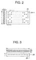
- Fig. 2 shows the relationship between the mask 26 and the cross-sectional shape (shown by hatching) of a linear laser beam, which is converted in the conversion optical system 24.
- the mask 26 has a processing pattern including a plurality of holes 26-1 that are arranged at random or regularly at a given pitch P with respect to the direction of the movement shown by an arrow.
- the width W is larger than the diameter of the holes 26-1 and the length L is larger than the range of the processing pattern in the width direction of the mask 26.
- the mask 26 moves across the linear laser beam so that a plurality of laser beam components passing through the holes 26-1 lying in one row of the mask 26 reach the work 27 through the imaging lens 28. Since the mask stage 25 and the work stage 29 are controlled so that these move synchronously in the opposite directions along the same axial direction, holes are continuously formed in the work 27 for every row of the processing pattern of the mask 26 in sequence.
- the pulse frequency of the laser beam from the CO 2 laser oscillator 21 is set so as to be synchronized with the movement corresponding to one pitch of the mask stage 25.
- the holes 26-1 in the same row are irradiated with the laser beam at least one time or two times, if necessary, depending on the energy intensity of the laser beam. This means that the same region in the work 27 is irradiated with the laser beam at least one time or two times if necessary. As a result, holes are formed in the region irradiated with the laser beam.
- the laser beam is fixed while the mask stage 25 and the work stage 29 are movable.
- a mask 26' having a row of holes 26-1' is used. In this case, it is not necessary to drive the mask stage during laser irradiation.
- the linear laser beam from the conversion optical system 24 is incident on the mask 26', which is always fixed, whereas only the work stage 29 moves in the direction of an arrow in Fig. 3.
- the mask 26 may be fixed while the work 27 is irradiated with a linear laser beam that is scanned on the mask 26 in one axial direction by a galvano-scanner.
- the galvano-scanner is provided between the conversion optical system 24 and the mask 26.
- the work stage 29 moves the subsequent processing region to a scanning region by the galvano-scanner.
- the diameter of the holes formed by the above-mentioned drilling is in the range of about 30 to 300 ⁇ m.
- the diameter of the holes 26-1 formed in the mask 26 is also in the range of 30 to 300 ⁇ m.
- the mask 26 is generally formed of a metallic material and the holes have an aspect ratio (ratio of the diameter to the depth of the hole) of about 1.
- the thickness of the mask 26 is also 50 ⁇ m. The same relationship applies to the mask 26' shown in Fig. 3.
- an increased density of the holes 26-1 impairs heat dissipation during laser beam irradiation, resulting in the thermal deformation of the mask 26.
- the deformation of the mask 26 causes the difference of the positions and the distortion of the shape of the holes formed.
- an object of the present invention is to provide a mask for laser processing which does not cause thermal deformation during irradiation with a laser beam.
- Another object of the present invention is to provide a method for making the mask.
- Still another object of the present invention is to provide a laser processing apparatus using the mask.
- a mask for laser processing according to the present invention has a predetermined processing pattern.
- the mask comprises a mask member having the processing pattern and comprised of a material that reflects laser light and substrate members for holding the mask member on both faces thereof and comprised of a material that transmits the laser light.
- the above-mentioned laser light is, for example, infrared light
- the mask member comprises one of Au, Cu, Ni, and beryllium-copper
- the substrate members comprise one of Ge, ZnS, and ZnSe.
- a laser processing apparatus carries out processing defined by a predetermined processing pattern to a work by irradiating the work with a laser beam from a laser oscillator thorough a mask having the predetermined pattern.
- the mask also comprises a mask member having the processing pattern and comprised of a material that reflects laser light and substrate members for holding the mask member on both faces thereof and comprised of a material that transmits the laser light.
- the above-mentioned laser oscillator is a CO 2 laser oscillator
- the mask member comprises one of Au, Cu, Ni, and beryllium-copper
- the substrate members comprise one of Ge, ZnS, and ZnSe.
- a method for making a mask for laser processing having a predetermined processing pattern comprises a first step of forming a material layer comprising a material that reflects laser light on one face of a first substrate member comprising a material that transmits the laser light, a second step of forming the processing pattern in the material layer, and a third step of bonding a second substrate member comprising a material that transmits the laser light to a face, which is not in contact with the first substrate, of the material layer provided with the processing pattern.
- the above-mentioned first step is performed by a vacuum evaporation or plating process, and the second step is performed by lithography, etching, or laser processing.
- high-frequency vibrations are applied to at least one of the assembly of the material layer provided with the processing pattern and the first substrate member and the second substrate member to bond them.
- the laser oscillator is the CO 2 laser oscillator shown in Fig. 1.
- Au is deposited on one face of a Ge substrate member 11 (first substrate member) having high transmittance for the wavelengths of the CO 2 laser beam (9.3 ⁇ m, 9.4 ⁇ m, 10.6 ⁇ m, or the like) to form a mask member layer 12 having a thickness of about 50 ⁇ m, by vacuum evaporation.
- a plating process may be employed instead of the vacuum evaporation process.
- a plurality of holes 12-1 having a diameter of 50 ⁇ m that define the processing pattern are formed in the mask member layer 12 by a well known combination of lithography and etching or by direct laser processing.
- a substrate member 13 (second substrate membr) is placed onto a face, which is not in contact with the substrate member 11, of the mask member layer 12 to bond them.
- a bonding method at least one of the substrate member 13 and the assembly of the substrate member 11 and the mask member layer 12 is vibrated in a direction parallel to the plane at a high frequency.
- the mask member layer 12 and the substrate member 13 are bonded to each other by frictional heat generated therebetween.
- a mask 10 that has a plurality of holes 12-1 having a diameter of 50 ⁇ m and an aspect ratio of 1 is obtained.
- the thickness of the first and second substrates 11 and 13, respectively, is in the range of about several tens of ⁇ m to several hundred ⁇ m.
- portions corresponding to the holes 12-1 are composed of only Ge and thus have high transmittance for the laser beam. Since Au has high reflectance for the laser beam, the heat absorbed dissipates through the first and second substrates 11 and 13, and the mask 10 is not heated to a high temperature, and therefore no deformation is caused. Furthermore, the first and second substrates 11 and 13 mechanically prevent thermal deformation of the mask member layer 12 therebetween.
- Materials for each component of the mask 10 are as follows.
- Materials for the first and second substrates 11 and 13 include Ge, ZnS (zinc sulfide), and ZnSe (zinc selenide).
- Materials for the mask member layer 12 include Au, Cu, Ni, and beryllium-copper.
- Preferred combinations are Ge-Au, Ge-Cu, and Ge-Ni. In the case of Ge-Au, these are immiscible with each other and form a eutectic alloy.
- the eutectic composition contains 17 atomic percent Ge and is a low-melting-point alloy having a eutectic point of 356°C.
- Ge-Cu In the case of Ge-Cu, about 10 atomic percent Ge is dissolved into Cu. In the region containing a larger amount of Ge, various intermetallic compounds are formed. At a Ge content of about 25 atomic percent or more, a eutectic alloy (having a eutectic point of about 640°C) of Cu 3 Ge and Ge is formed.
- Ge-Ni In the case of Ge-Ni, about 12 atomic percent Ge is dissolved into Ni. In the region containing a larger amount of Ge, various intermetallic compounds are formed. At a Ge content of about 50 atomic percent or more, a eutectic alloy (having a eutectic point of about 780°C) of NiGe and Ge is formed.
- the Ge-Au system is most preferred because an alloy is readily formed. However, it should be noted that this alloy melts at a low temperature of 356°C. Since Ge and Au readily form a eutectic alloy, a homogeneous structure of Ge and Au exhibits high thermal conductivity. In addition, a small amount of heat generated in Au due to laser beam absorption readily dissipates through the first and second substrates 11 and 13.
- the mask according to the above embodiments is suitable for the mask 26 of the laser drilling apparatus for carrying out the drilling to the resin layer of the printed circuit board shown in Fig. 1.
- the mask according to the present invention is not limited to the mask of the laser drilling apparatus.
- this is also applicable to a mask of a laser distortion processing apparatus that irradiates a plurality of fine ceramic substrates arranged in a row with a plurality of laser beams to impart microdistorsion to each ceramic substrate.
- the laser oscillator is not limited to the CO 2 laser oscillator.
- Other laser oscillators for example, a YAG laser oscillator and a YLF laser oscillator can also be used.
- Materials for the first and second substrate and the mask member layer may be selected depending on the laser oscillator.
- the first and second substrates dissipate heat from the mask member layer and mechanically fix the mask member layer; hence, the resulting mask for laser drilling does not undergo thermal deformation due to irradiation with laser light.
- the mask according to the present invention is suitable for a mask of a laser drilling apparatus for carrying out the drilling to a work and a mask of a laser distortion processing apparatus for imparting distortion to a work.
Landscapes
- Physics & Mathematics (AREA)
- Optics & Photonics (AREA)
- Engineering & Computer Science (AREA)
- Plasma & Fusion (AREA)
- Mechanical Engineering (AREA)
- General Physics & Mathematics (AREA)
- Laser Beam Processing (AREA)
Abstract
Description
Claims (7)
- A mask for laser processing having a predetermined processing pattern, the mask comprising a mask member having the processing pattern and comprised of a material that reflects laser light and substrate members for holding the mask member on both faces thereof and comprised of a material that transmits the laser light.
- The mask for laser processing according to claim 1, wherein the laser light is infrared light, the mask member comprises one of Au, Cu, Ni, and beryllium-copper, and the substrate members comprise one of Ge, ZnS, and ZnSe.
- A laser processing apparatus for carrying out processing defined by a predetermined processing pattern to a work by irradiating the work with a laser beam from a laser oscillator thorough a mask having the predetermined pattern, wherein the mask comprises:a mask member having the processing pattern and comprised of a material that reflects laser light and substrate members for holding the mask member on both faces thereof and comprised of a material that transmits the laser light.
- The laser processing apparatus according to claim 3, wherein the laser oscillator is a CO2 laser oscillator, the mask member comprises one of Au, Cu, Ni, and beryllium-copper, and the substrate members comprise one of Ge, ZnS, and ZnSe.
- A method for making a mask for laser processing having a predetermined processing pattern, the method comprising:a first step of forming a material layer comprising a material that reflects laser light on one face of a first substrate member comprising a material that transmits the laser light;a second step of forming the processing pattern in the material layer; anda third step of bonding a second substrate member comprising a material that transmits the laser light to a face, which is not in contact with the first substrate, of the material layer provided with the processing pattern.
- The method for making a mask for laser processing according to claim 5, wherein the first step is performed by a vacuum evaporation or plating process, and the second step is performed by lithography, etching, or laser processing.
- The method for making a mask for laser processing according to claim 5, wherein, in the third step, high-frequency vibrations are applied to at least one of the assembly of the material layer provided with the processing pattern and the first substrate member and the second substrate member to bond them.
Applications Claiming Priority (3)
| Application Number | Priority Date | Filing Date | Title |
|---|---|---|---|
| JP2000019505A JP3348283B2 (en) | 2000-01-28 | 2000-01-28 | Laser processing apparatus, laser processing mask, and method of manufacturing the same |
| JP2000019505 | 2000-01-28 | ||
| PCT/JP2001/000039 WO2001054855A1 (en) | 2000-01-28 | 2001-01-09 | Laser machining device and laser machining mask and production method therefor |
Publications (2)
| Publication Number | Publication Date |
|---|---|
| EP1262271A1 true EP1262271A1 (en) | 2002-12-04 |
| EP1262271A4 EP1262271A4 (en) | 2009-11-11 |
Family
ID=18546193
Family Applications (1)
| Application Number | Title | Priority Date | Filing Date |
|---|---|---|---|
| EP01900631A Withdrawn EP1262271A4 (en) | 2000-01-28 | 2001-01-09 | Laser machining device and laser machining mask and production method therefor |
Country Status (7)
| Country | Link |
|---|---|
| US (1) | US6906282B2 (en) |
| EP (1) | EP1262271A4 (en) |
| JP (1) | JP3348283B2 (en) |
| KR (1) | KR100493117B1 (en) |
| CN (2) | CN1275292C (en) |
| TW (1) | TW470680B (en) |
| WO (1) | WO2001054855A1 (en) |
Families Citing this family (26)
| Publication number | Priority date | Publication date | Assignee | Title |
|---|---|---|---|---|
| TW521310B (en) * | 2001-02-08 | 2003-02-21 | Toshiba Corp | Laser processing method and apparatus |
| CN1328009C (en) * | 2001-08-02 | 2007-07-25 | 株式会社Skc | Method for fabricating chemical mechanical polishing pad using laser |
| US7468557B2 (en) * | 2002-09-11 | 2008-12-23 | Syracuse University | Method of producing an ultra thin electrically conducting film with very low electrical resistance |
| JP2004243404A (en) * | 2003-02-17 | 2004-09-02 | Internatl Business Mach Corp <Ibm> | Hole forming method and hole forming apparatus |
| US7671297B2 (en) * | 2003-11-20 | 2010-03-02 | Ethicon, Inc. | Method and apparatus for laser drilling workpieces |
| DE102004036662B3 (en) * | 2004-07-28 | 2006-05-04 | Lpkf Laser & Electronics Ag | Method for penetrating apertures in a stencil or mask |
| KR20120103651A (en) * | 2009-12-23 | 2012-09-19 | 아이엠알에이 아메리카, 인코포레이티드. | Laser patterning using a structured optical element and focused beam |
| KR101097328B1 (en) * | 2010-01-07 | 2011-12-23 | 삼성모바일디스플레이주식회사 | Laser beam irradiation apparatus for substrate sealing, substrate sealing method, and manufacturing method of organic light emitting display device using the same |
| JP6046329B2 (en) * | 2010-01-08 | 2016-12-14 | 早川ゴム株式会社 | Joining method using laser light |
| KR101135537B1 (en) * | 2010-07-16 | 2012-04-13 | 삼성모바일디스플레이주식회사 | Laser irradiation apparatus |
| JP5746960B2 (en) * | 2011-12-15 | 2015-07-08 | 豊田鉄工株式会社 | Infrared heating device |
| KR101200484B1 (en) * | 2012-03-21 | 2012-11-12 | 한국기계연구원 | Mask for projection ablation and manufacturing method thereof |
| CN104640576B (en) * | 2012-05-29 | 2017-04-19 | 3M创新有限公司 | Absorbent articles including polymeric foams and intermediates |
| US20150301444A1 (en) * | 2012-06-18 | 2015-10-22 | Indian Institute Of Technology Kanpur | Systems and methods for dry processing fabrication of binary masks with arbitrary shapes for ultra-violet laser micromachining |
| CN103529507B (en) * | 2012-07-06 | 2016-05-25 | 三菱电机株式会社 | Polarised light polarizer and laser machine |
| JP5936574B2 (en) * | 2012-07-06 | 2016-06-22 | 三菱電機株式会社 | Polarization phase difference plate and laser processing machine |
| JP6142194B2 (en) * | 2012-11-15 | 2017-06-07 | 株式会社ブイ・テクノロジー | Vapor deposition mask manufacturing method and vapor deposition mask |
| JP5958824B2 (en) * | 2012-11-15 | 2016-08-02 | 株式会社ブイ・テクノロジー | Manufacturing method of vapor deposition mask |
| KR20140133741A (en) * | 2013-05-10 | 2014-11-20 | 삼성디스플레이 주식회사 | Liti mask and laser irradiation device including thereof |
| JP6240960B2 (en) * | 2014-02-03 | 2017-12-06 | 株式会社ブイ・テクノロジー | Method for manufacturing film formation mask and film formation mask |
| RU2661977C1 (en) * | 2014-07-03 | 2018-07-23 | Ниппон Стил Энд Сумитомо Метал Корпорейшн | Laser processing apparatus |
| KR102374204B1 (en) * | 2016-03-25 | 2022-03-14 | 삼성전자주식회사 | Method of manufacturing semiconductor device |
| KR20180089607A (en) * | 2017-01-31 | 2018-08-09 | 삼성디스플레이 주식회사 | Method of manufacturing mask for deposition |
| CN108941921A (en) * | 2018-07-10 | 2018-12-07 | 嘉善县飞虹钮扣厂 | A kind of device of button surface textures |
| JP7303053B2 (en) * | 2019-07-17 | 2023-07-04 | ファナック株式会社 | Adjustment aid and laser welding equipment |
| KR102394825B1 (en) * | 2020-04-23 | 2022-05-06 | 주식회사 프로텍 | Flip Chip Bonding Apparatus Using VCSEL Device |
Family Cites Families (10)
| Publication number | Priority date | Publication date | Assignee | Title |
|---|---|---|---|---|
| US4478677A (en) * | 1983-12-22 | 1984-10-23 | International Business Machines Corporation | Laser induced dry etching of vias in glass with non-contact masking |
| JP2521299B2 (en) | 1987-08-18 | 1996-08-07 | 三菱電機株式会社 | Character mask for laser mark |
| US4887283A (en) * | 1988-09-27 | 1989-12-12 | Mitsubishi Denki Kabushiki Kaisha | X-ray mask and exposure method employing the same |
| JP2592369B2 (en) | 1991-08-22 | 1997-03-19 | 富士通株式会社 | Method for manufacturing multilayer wiring circuit board and method for manufacturing dielectric mirror mask |
| SG52140A1 (en) * | 1994-03-04 | 1998-09-28 | Canon Kk | Ink jet recording head and method of manufacture therefor and laser processing apparatus and ink jet recording apparatus |
| JPH0876357A (en) | 1994-09-01 | 1996-03-22 | Hitachi Ltd | Laser transfer mask |
| TW289901B (en) * | 1994-12-28 | 1996-11-01 | Ricoh Microelectronics Kk | |
| US6211485B1 (en) * | 1996-06-05 | 2001-04-03 | Larry W. Burgess | Blind via laser drilling system |
| JPH11277282A (en) * | 1998-03-30 | 1999-10-12 | Toppan Forms Co Ltd | Optical shutter device |
| JP2000122266A (en) * | 1998-10-13 | 2000-04-28 | Oki Electric Ind Co Ltd | Pellicle |
-
2000
- 2000-01-28 JP JP2000019505A patent/JP3348283B2/en not_active Expired - Fee Related
-
2001
- 2001-01-09 KR KR10-2002-7009627A patent/KR100493117B1/en not_active Expired - Fee Related
- 2001-01-09 CN CNB2004100644043A patent/CN1275292C/en not_active Expired - Fee Related
- 2001-01-09 CN CNB018042554A patent/CN1170654C/en not_active Expired - Fee Related
- 2001-01-09 EP EP01900631A patent/EP1262271A4/en not_active Withdrawn
- 2001-01-09 US US10/181,423 patent/US6906282B2/en not_active Expired - Fee Related
- 2001-01-09 WO PCT/JP2001/000039 patent/WO2001054855A1/en not_active Ceased
- 2001-01-15 TW TW090100855A patent/TW470680B/en not_active IP Right Cessation
Also Published As
| Publication number | Publication date |
|---|---|
| US20030000930A1 (en) | 2003-01-02 |
| JP3348283B2 (en) | 2002-11-20 |
| HK1071326A1 (en) | 2005-07-15 |
| HK1053277A1 (en) | 2003-10-17 |
| CN1170654C (en) | 2004-10-13 |
| CN1569381A (en) | 2005-01-26 |
| TW470680B (en) | 2002-01-01 |
| KR20020071969A (en) | 2002-09-13 |
| WO2001054855A1 (en) | 2001-08-02 |
| EP1262271A4 (en) | 2009-11-11 |
| CN1275292C (en) | 2006-09-13 |
| JP2001205470A (en) | 2001-07-31 |
| CN1396851A (en) | 2003-02-12 |
| US6906282B2 (en) | 2005-06-14 |
| KR100493117B1 (en) | 2005-06-02 |
Similar Documents
| Publication | Publication Date | Title |
|---|---|---|
| US6906282B2 (en) | Laser processing apparatus, mask for laser processing, and method for making the mask | |
| US5367143A (en) | Apparatus and method for multi-beam drilling | |
| JP5816409B2 (en) | Method to increase throughput for laser via drilling | |
| KR100268681B1 (en) | Method and apparatus for processing ceramic green sheet | |
| KR100367856B1 (en) | Method For Machining Ceramic Green Sheet And Apparatus For Machining The Same | |
| KR100530818B1 (en) | Method and device for laser beam machining of laminated material | |
| KR100477147B1 (en) | Method and apparatus for laser drilling | |
| KR20010095011A (en) | Method and apparatus using laser pulses to make an array of microcavity holes | |
| US6833528B2 (en) | Method and apparatus for laser processing | |
| JPH11309594A (en) | Laser processing device and its processed parts | |
| JP3175006B2 (en) | Laser processing apparatus and processing method | |
| US6583380B2 (en) | Device and method for marking copper-clad laminates | |
| JP3458760B2 (en) | Processing method of ceramic green sheet | |
| JP3385504B2 (en) | Laser processing apparatus and irradiation method using laser processing apparatus | |
| JP3353134B2 (en) | Laser processing equipment | |
| HK1053277B (en) | Laser machining mask and production method therefor | |
| HK1071326B (en) | Laser machining mask and production method therefor | |
| JPS62168688A (en) | Laser beam machining device | |
| JP2001162392A (en) | Laser drilling method and processing device | |
| JP2004098121A (en) | Laser processing method and laser processing apparatus | |
| JP2003211276A (en) | Laser processing method and laser processing apparatus | |
| JPH11333585A (en) | Desmear apparatus and desmear method for laser drilling machine | |
| HK1040953A1 (en) | Device and method for marking copper-clad laminates |
Legal Events
| Date | Code | Title | Description |
|---|---|---|---|
| PUAI | Public reference made under article 153(3) epc to a published international application that has entered the european phase |
Free format text: ORIGINAL CODE: 0009012 |
|
| 17P | Request for examination filed |
Effective date: 20020729 |
|
| AK | Designated contracting states |
Kind code of ref document: A1 Designated state(s): AT BE CH CY DE DK ES FI FR GB GR IE IT LI LU MC NL PT SE TR |
|
| RBV | Designated contracting states (corrected) |
Designated state(s): AT BE CH CY DE FI FR IT LI NL |
|
| A4 | Supplementary search report drawn up and despatched |
Effective date: 20091008 |
|
| RIC1 | Information provided on ipc code assigned before grant |
Ipc: G02B 27/09 20060101ALI20091002BHEP Ipc: B23K 26/06 20060101AFI20010809BHEP Ipc: G03F 1/08 20060101ALI20091002BHEP |
|
| STAA | Information on the status of an ep patent application or granted ep patent |
Free format text: STATUS: THE APPLICATION IS DEEMED TO BE WITHDRAWN |
|
| 18D | Application deemed to be withdrawn |
Effective date: 20100108 |