EP1261127A2 - Semiconductor integrated circuit device - Google Patents
Semiconductor integrated circuit device Download PDFInfo
- Publication number
- EP1261127A2 EP1261127A2 EP01119610A EP01119610A EP1261127A2 EP 1261127 A2 EP1261127 A2 EP 1261127A2 EP 01119610 A EP01119610 A EP 01119610A EP 01119610 A EP01119610 A EP 01119610A EP 1261127 A2 EP1261127 A2 EP 1261127A2
- Authority
- EP
- European Patent Office
- Prior art keywords
- long
- circuit
- distance wiring
- wiring
- semiconductor integrated
- Prior art date
- Legal status (The legal status is an assumption and is not a legal conclusion. Google has not performed a legal analysis and makes no representation as to the accuracy of the status listed.)
- Withdrawn
Links
Images



Classifications
-
- G—PHYSICS
- G11—INFORMATION STORAGE
- G11C—STATIC STORES
- G11C11/00—Digital stores characterised by the use of particular electric or magnetic storage elements; Storage elements therefor
- G11C11/21—Digital stores characterised by the use of particular electric or magnetic storage elements; Storage elements therefor using electric elements
- G11C11/34—Digital stores characterised by the use of particular electric or magnetic storage elements; Storage elements therefor using electric elements using semiconductor devices
- G11C11/40—Digital stores characterised by the use of particular electric or magnetic storage elements; Storage elements therefor using electric elements using semiconductor devices using transistors
- G11C11/401—Digital stores characterised by the use of particular electric or magnetic storage elements; Storage elements therefor using electric elements using semiconductor devices using transistors forming cells needing refreshing or charge regeneration, i.e. dynamic cells
- G11C11/406—Management or control of the refreshing or charge-regeneration cycles
-
- H—ELECTRICITY
- H03—ELECTRONIC CIRCUITRY
- H03K—PULSE TECHNIQUE
- H03K5/00—Manipulating of pulses not covered by one of the other main groups of this subclass
- H03K5/15—Arrangements in which pulses are delivered at different times at several outputs, i.e. pulse distributors
- H03K5/15013—Arrangements in which pulses are delivered at different times at several outputs, i.e. pulse distributors with more than two outputs
Definitions
- the present invention relates to a semiconductor integrated circuit device and in particular to a semiconductor integrated circuit device having a large chip size and a fine wiring in which a ratio of a wiring delay in a critical path delay time is reduced, thereby improving the operation speed.
- the speed of a critical path including a long-distance wiring in a semiconductor integrated circuit device has been improved by (a) improvement of a load drive force of a gate circuit, (b) increase of width of the long-distance wiring, (c) dispersion of output load by gate circuit multiplication, and the like.
- the speed increasing methods (a) to (c) can have a significant effect.
- Method (a) can have a significant effect while the wiring resistance is sufficiently small as compared to the operation resistance of the load drive transistor of the gate circuit but the wiring resistance cannot be ignored as compared to the operation resistance of the load drive transistor of the gate circuit as the chip size becomes greater and the wiring becomes finer.
- method (a) can have an effect for the capacity load but cannot have a significant effect for the resistance load such as the wiring resistance.
- Method (b) is usually used together with method (a). That is, when method (b) is used to increase the wiring width and reduce the wiring resistance, the load capacity component is increased and accordingly, method (a) is used to increase the speed of the gate circuit for driving the long-distance wiring. However, when the wiring width is increased, although the wiring resistance is reduced, the wiring capacity is increased.
- method (a) has a limitation from the viewpoint of the area overhead or the power consumption and the effect of increasing the speed is not sufficient.
- Method (c) or a technique of inserting a relay buffer in the middle of the long-distance wiring for increasing the speed also has a problem that two stages of inverter should be inserted for matching the signal polarity and increasing the speed in all cases is impossible due to the area problem.
- the present invention employs means as follows in order to achieve the aforementioned object.
- the present invention provides a semiconductor integrated circuit device including a driver circuit 100, a first long-distance wiring 104 connected to the driver circuit 100, and a plurality of gate circuits 103 distributed over and connected to the entire length of the first long-distance wiring 104, wherein an output signal of the driver circuit 100 is received via the first long-distance wiring 104 by the plurality of gate circuits 103, and the driver circuit 100 has an input circuit connected to a node 105 in the vicinity of an input terminal of the gate circuit 103 connected to the end of the first long-distance wiring 104 using a second long-distance wiring 106 and a speed-increasing circuit 107.
- a signal change is accelerated not only from one end of the driver circuit 100 but also from the other end by using a second long-distance wiring 106 and a speed-increasing circuit 107 from an early stage, thereby enabling to significantly reduce the wiring delay time and increase the critical path speed as well as to improve the operation speed of the semiconductor integrated circuit device.
- a waveform in the vicinity of the long-distance wiring end is driven by the speed-increasing circuit arranged physically in the vicinity, the waveform becomes sharp and a high-speed response of the receiver circuit can be obtained.
- Fig. 1 shows a semiconductor integrated circuit device according to a first embodiment of the present invention.
- VIN denotes an input signal
- 100 denotes a driver circuit having a CMOS inverter 101
- 104 denotes a first long-distance wiring
- 103 denotes a plurality of subsequent-stage gate circuits connected at approximately identical interval on the first long-distance wiring 104
- 106 denotes a second long-distance wiring
- 107 denotes a speed-increasing circuit having a PMOS transistor 108.
- This configuration is characterized in that for example, in a drive method for all-at-once driving a plenty of fan-outs and a long-distance wiring such as a memory word line drive method, i.e., in the configuration of the driver circuit 100 for driving the first long-distance wiring 104 and the plurality of gate circuits 103, an input of the driver circuit 100 and an end node 105 of the first long-distance wiring 104 (the node 105 in the vicinity of the input terminal of the gate circuit 103 arranged physically at the farthest end viewed from an output node 102 of the CMOS inverter 101) is by-passed using the second long-distance wiring 106 and the speed-increasing circuit 107.
- a drive method for all-at-once driving a plenty of fan-outs and a long-distance wiring such as a memory word line drive method
- the output node 102 of the CMOS inverter 101 is changed from low to high, and the node 105 is also changed from low to high.
- the time (wiring delay time) required for the signal change of the node 102 to reach the node 105 is approximately a product of the wiring resistance of the long-distance wiring 104 and the entire capacitance formed on the long-distance wiring 104 (total of the wiring capacity of the long-distance wiring and the input capacity of the plurality of gate circuits 103 which are fan-out of the CMOS inverter 101).
- the input signal VIN is changed from high to low
- the input node 109 of the speed-increasing circuit 107 via the second long-distance wiring 106 is also changed from high to low.
- the PMOS transistor 108 turns on to increase the potential of the node 105 to high in the same way as the drive of the aforementioned CMOS inverter 101.
- the wiring delay time of the second long-distance wiring 106 is by far shorter than the first long-distance wiring 104 because there is no gate circuit 103 connected as a fan out.
- the signal change start time from high to low of the node 109 is by far earlier than the signal change start time of the node 105 changed by the output signal transferred through the long-distance wiring 104 by drive of the CMOS inverter 101 and accordingly, the node 105 can start the signal change by the speed-increasing circuit 107 without waiting for the signal sent through the first long-distance wiring 104.
- the PMOS transistor 108 in the speed-increasing circuit 107 is cut off and the potential of the node 105 is driven only by the CMOS inverter 101 and pulled down from high to low by the first long-distance wiring 104.
- Fig. 2 shows a second embodiment of the present invention.
- the speed-increasing circuit 107 explained in the first embodiment is realized by an NMOS transistor 110 instead of the PMOS transistor 108.
- a buffer circuit 111 is provided at the input side of the second long-distance wiring 106 for polarity matching.
- the other parts of the configuration are identical as the first embodiment. With this configuration, it is possible to obtain the same effect as the aforementioned first embodiment.
- the first long-distance wiring 104 has an opposite polarity of the second long-distance wiring 106 and there is a danger of generation of a cross talk between the two of the long-distance wiring.
- the polarities are identical and there is no danger of generating a cross talk between the two of the long-distance wiring.
- Fig. 3 shows the third embodiment of the present invention.
- the signal change is accelerated by providing the speed-increasing circuit 107 at the node 105 in the vicinity of the input terminal of the gate circuit 103 arranged physically at the farthest end viewed from the output node 102 of the CMOS inverter 101.
- a path passing through a node in the vicinity of the input terminal of the gate circuit 103 arranged in the middle of the first long-distance wiring 104 becomes a critical path. Accordingly, by additionally inserting a speed-increasing circuit 107 at the position of the node 112 in the vicinity of that gate circuit 103, it is possible to obtain a higher speed than in the first embodiment.
- This third embodiment of the present invention is shown in Fig. 3.
- a single speed-increasing circuit 107 is additionally inserted at the middle of the first long-distance wiring 104 but by further inserting such circuits, it is possible to further reduce the wiring delay time. Any number of speed-increasing circuit 107 may be inserted. The number of the speed-increasing circuits 107 inserted and their size may be selected so as to minimize the wiring delay time while considering the number of the fan outs of the driver circuit 100, and the wiring line width connected to the output of the driver circuit 100. This embodiment has an effect to selectively increase the speed of the critical path using simple means.
- Fig. 4 shows a first application example of the present invention.
- This application example for applying the third embodiment to the clock distribution method employs a clock input signal VCK as the input signal VIN, a clock driver as the driver circuit 100, and a flip-flop circuit 203 as the gate circuit.
- an input of the clock driver circuit 100 is connected to a clock input terminal CK of the flip-flop circuits 203 in the farthest end and at the middle viewed from the clock driver circuit 100 (CMOS inverter 101) at the speed-increasing circuit (inverter circuit) 107.
- Fig. 5 shows a fourth embodiment of the present invention.
- the fourth embodiment has a basic configuration identical to the first embodiment (Fig. 1) except for a buffer circuit 200 and a buffer circuit 201 arranged between an input of the driver circuit 100 and an input side end of the second long-distance wiring 106.
- the load driven by the driver circuit 100 includes an input capacity of the CMOS inverter 101 and a wiring capacity and resistance of the second long-distance wiring 106.
- the load of this second long-distance wiring 106 remarkably increases the delay of the input signal VIN from the drive circuit, eliminating the effect of the speed increase, the present embodiment has a significant effect.
- the buffer circuit 201 can drive the long-distance wiring 106 and the speed-increasing circuit 107 without deteriorating the delay of the input signal VIN.
- a delay overhead equivalent two stages of a buffer circuit is present, by tuning the element device, power source voltage, process, or the buffer circuit and the speed-increasing circuit element size, it is possible to obtain a greater effect than the speed increase by the first embodiment.
- the operation is identical as the first embodiment and its explanation is omitted here.
- the drive method for all-at-once driving a plenty of fan outs and long-distance wiring lines may be a clock distribution method (used in the first application example) having a clock driver for driving a plurality of flip-flops, a memory word line drive method (used in the second application example as will be detailed later), or a path including a driver for driving a plurality of selector circuit control lines.
- a clock distribution method used in the first application example
- a memory word line drive method used in the second application example as will be detailed later
- a path including a driver for driving a plurality of selector circuit control lines it is possible to obtain the effects explained in the first to the fourth embodiments and improve the operation speed.
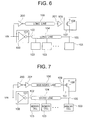
- Fig. 6 shows a fifth embodiment of the present invention.
- This embodiment differs from the aforementioned circuit configuration of the fourth embodiment (Fig. 5) in that the buffer circuit 201 is arranged after the second long-distance wiring 106. That is, by using the buffer circuit 201 to correct the voltage waveform which has passed through the second long-distance wiring 106, before passing the voltage waveform to the speed-increasing circuit 107, the response characteristic of the PMOS transistor 108 is improved. This also increases the voltage response of the node 105 and further reduces the wiring delay of the long-distance wiring 104.
- Fig. 7 shows the second application example of the present invention.
- the circuit configuration is completely identical to that of the fourth embodiment.
- the gate circuit 103 is realized by a memory cell 303
- the first long-distance wiring line 104 is realized by a word line WL
- the second long-distance wiring 106 is realized by a sub-word line.
- the memory cell 303 is activated to read out or write in data (word line selected state) when the input signal VIN is changed from high to low and the word line WL 104 is changed from low to high.
- the word line WL 104 is changed from high to low, the memory cell is dis-activated and does not perform data read out or write in (word line non-selected state).
- the figure shows two operation waveforms of the node 105.
- the waveform shown by a dotted line is a waveform obtained when not providing a by-pass circuit including buffer circuits 200 and 201, the sub-word line 106, and the PMOS transistor 108.
- the node 105 in the vicinity of the input terminal of the memory cell 303 arranged at the farthest bit viewed from the word line driver 100 is also changed from low to high after the wiring delay time of the word line 104.
- the waveform in the dotted line a dull rise. Accordingly, the response of the memory cell receiving the waveform is slow and the wiring delay time of the word line is great.
- the waveform of the node 105 shown by a solid line when the input signal VIN is changed from high to low, the node 109 via the buffer circuits 200 and 201 and the sub-word line 106 is also changed from high to low, and the PMOS transistor 108 turns on.
- the word line 104 and the sub-word line 106 have an identical length but the sub-word line 106 has a by far shorter wiring delay time than the word line 104 because no memory cell 303 is connected as fan outs for the number of bits.
- the voltage waveform of the node 105 starts rising at an early time as compared to the waveform shown by a dotted line in the figure.
- the waveform rises sharply as compared to the waveform shown by a dotted line, like the rising waveform of the node 102.
- the memory cell 303 rapidly reads out, thereby significantly reducing the wiring delay time of the word line WL.
- the input signal VIN turns from low to high (word line non-selected state)
- the output node 102 of the word line driver 100 turns from high to low.
- the memory cell 303 is dis-activated and does not perform data read out.
- the PMOS transistor 108 is cut out and the trailing waveform of the node 105 is identical in the dotted line and the solid line in the figure.
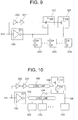
- Fig. 9 shows a third application example of the present invention.
- This application example is a combination of the third embodiment (Fig. 3) and the fourth embodiment (Fig. 5) which is applied to the clock distribution method.
- VCK represents a clock input signal
- 100 represents a clock driver circuit
- 203 represents a flip-flop circuit.
- clock input terminals CK of the flip-flop circuit 203 arranged at the farthest end and in the middle viewed from the output of the clock driver circuit 100 are connected by the speed-increasing circuit 107.
- the speed-increasing circuit 107 is inserted at two positions but may be inserted at more positions as has been detailed in the third embodiment and the explanation is omitted here.
- Fig. 10 shows a sixth embodiment of the present invention.
- the speed-increasing circuit 107 explained in the fourth embodiment (Fig. 5) is replaced by a speed-increasing circuit 113 including a CMOS inverter having a PMOS transistor 114 and an NMOS transistor 115.
- the operation differs from that of the fourth embodiment in the operation of the speed-increasing circuit 113.
- an input node 109 of the speed-increasing circuit 113 via the buffer circuits 200 and 201 and the second long-distance wiring 106 is also changed from low to high and the NMOS transistor of the speed-increasing circuit 113 turns on, thereby decreasing the potential of the node 105 to low (grounding potential) (at this moment, the PMOS transistor 114 is off).
- the input node 109 of the speed-increasing circuit 113 is also changed from high to low and the PMOS transistor of the speed-increasing circuit 113 turns on, thereby increasing the potential of the node 105 to high (power supply potential (at this moment, the NMOS transistor 115 is off).
- this embodiment Since this embodiment operates as has been described above, this embodiment enables to obtain a high-speed operation at the long-distance wiring voltage change trail in the same way as at its rise in contrast to the aforementioned embodiments which enable to obtain a high-speed operation only at the rise of the long-distance wiring voltage change.
- the speed-increasing circuit 107 by configuring the speed-increasing circuit 107 as the present embodiment, it is possible to obtain a high speed in the word line non-selected state, too, as in the selected state.
Landscapes
- Physics & Mathematics (AREA)
- Nonlinear Science (AREA)
- Engineering & Computer Science (AREA)
- Microelectronics & Electronic Packaging (AREA)
- Computer Hardware Design (AREA)
- Design And Manufacture Of Integrated Circuits (AREA)
- Semiconductor Integrated Circuits (AREA)
- Dram (AREA)
Abstract
Description
Claims (9)
- A semiconductor integrated circuit device comprising a driver circuit (100), a first long-distance wiring (104) connected to the driver circuit (100), and a plurality of gate circuits (103) connected over the entire length of the first long-distance wiring (104), so that an input signal VIN is received by the plurality of gate circuits (103) via the driver circuit (100) and the first long-distance wiring (104),
wherein a node (105) arranged in the vicinity of an input terminal of the gate circuit connected to an input terminal of the driver circuit (100) and an end of the first long-distance wiring (104) is connected by a second long-distance wiring 106 and a speed-increasing circuit (107). - The semiconductor integrated circuit device as claimed in Claim 1, wherein the speed-increasing circuit (107) includes a PMOS transistor (108).
- The semiconductor integrated circuit device as claimed in Claim 1, wherein the speed-increasing circuit (107) includes an NMOS transistor (110) and a buffer circuit (111) is inserted at an input side of the second-long distance wiring.
- The semiconductor integrated circuit device as claimed in Claim 1, wherein the speed-increasing circuit (107) includes a CMOS inverter having a PMOS transistor (114) and an NMOS transistor (115).
- The semiconductor integrated circuit device as claimed in Claim 1, wherein a plurality of speed-increasing circuits (107) are additionally inserted between an intermediate position of the second long-distance wiring (106) and the vicinity of the input terminal of the gate circuit (103) connected to a position corresponding to that intermediate position.
- The semiconductor integrated circuit device as claimed in Claim 1, wherein a plurality of buffer circuits (200) and (201) are inserted at the input side of the second long-distance wiring (106).
- The semiconductor integrated circuit device as claimed in Claim 1, wherein a buffer circuit (200) is inserted at the input side of the second long-distance wiring (106), and a buffer circuit (201) is inserted at the output side of the second long-distance wiring (106).
- The semiconductor integrated circuit device as claimed in Claim 1, wherein the input signal VIN is realized by a word line selecting signal; the driver circuit (100) is realized by a word line driver; the first long-distance wiring (104) is realized by a word line WL; and the gate circuits (103) are realized by memory cells.
- The semiconductor integrated circuit device as claimed in Claim 1, wherein the input signal VIN is realized by a clock input signal VCK; the driver circuit (100) is realized by a clock driver; and the gate circuits (103) are realized by flip-flop circuits (203).
Applications Claiming Priority (2)
| Application Number | Priority Date | Filing Date | Title |
|---|---|---|---|
| JP2001155551 | 2001-05-24 | ||
| JP2001155551A JP2002353312A (en) | 2001-05-24 | 2001-05-24 | Semiconductor integrated circuit device |
Publications (2)
| Publication Number | Publication Date |
|---|---|
| EP1261127A2 true EP1261127A2 (en) | 2002-11-27 |
| EP1261127A3 EP1261127A3 (en) | 2004-10-20 |
Family
ID=18999716
Family Applications (1)
| Application Number | Title | Priority Date | Filing Date |
|---|---|---|---|
| EP01119610A Withdrawn EP1261127A3 (en) | 2001-05-24 | 2001-08-17 | Semiconductor integrated circuit device |
Country Status (4)
| Country | Link |
|---|---|
| US (1) | US6798255B2 (en) |
| EP (1) | EP1261127A3 (en) |
| JP (1) | JP2002353312A (en) |
| KR (1) | KR100426761B1 (en) |
Families Citing this family (5)
| Publication number | Priority date | Publication date | Assignee | Title |
|---|---|---|---|---|
| JP3776880B2 (en) * | 2002-12-10 | 2006-05-17 | 株式会社日立製作所 | Uninterruptible power system |
| JP4631743B2 (en) | 2006-02-27 | 2011-02-16 | ソニー株式会社 | Semiconductor device |
| WO2012077700A1 (en) * | 2010-12-10 | 2012-06-14 | 三菱瓦斯化学株式会社 | Polyester resin and optical lens |
| JP2018160855A (en) | 2017-03-23 | 2018-10-11 | 株式会社東芝 | Semiconductor device |
| JP7270451B2 (en) * | 2019-04-26 | 2023-05-10 | ルネサスエレクトロニクス株式会社 | Semiconductor device and method for driving semiconductor device |
Family Cites Families (14)
| Publication number | Priority date | Publication date | Assignee | Title |
|---|---|---|---|---|
| JPS6342216A (en) | 1986-08-08 | 1988-02-23 | Hitachi Ltd | Composite circuit containing bipolar transistor and field effect transistor |
| JPH02165724A (en) | 1988-12-19 | 1990-06-26 | Sharp Corp | Digital integrated circuit |
| JP3862346B2 (en) * | 1997-03-13 | 2006-12-27 | 富士通株式会社 | Driving circuit and semiconductor memory device using the same |
| US6472917B2 (en) * | 1997-03-19 | 2002-10-29 | Hitachi, Ltd. | Semiconductor integrated circuit device having compensation for wiring distance delays |
| WO1998042021A1 (en) | 1997-03-19 | 1998-09-24 | Hitachi, Ltd. | Semiconductor integrated circuit device |
| JPH11203858A (en) | 1998-01-05 | 1999-07-30 | Mitsubishi Electric Corp | Word line drive circuit and semiconductor memory device |
| JPH11260054A (en) * | 1998-01-08 | 1999-09-24 | Mitsubishi Electric Corp | Dynamic semiconductor memory device |
| JPH11317505A (en) | 1998-05-06 | 1999-11-16 | Hitachi Ltd | Semiconductor integrated circuit device |
| JP2000058785A (en) | 1998-08-07 | 2000-02-25 | Hitachi Ltd | Dynamic RAM |
| KR100281693B1 (en) | 1998-09-02 | 2001-02-15 | 윤종용 | High speed three phase booster circuit |
| JP2000243085A (en) | 1999-02-22 | 2000-09-08 | Hitachi Ltd | Semiconductor device |
| JP2000268563A (en) | 1999-03-16 | 2000-09-29 | Toshiba Corp | Semiconductor storage device |
| US6271713B1 (en) * | 1999-05-14 | 2001-08-07 | Intel Corporation | Dynamic threshold source follower voltage driver circuit |
| US6366520B1 (en) * | 2001-03-14 | 2002-04-02 | Micron Technology, Inc. | Method and system for controlling the slew rate of signals generated by open drain driver circuits |
-
2001
- 2001-05-24 JP JP2001155551A patent/JP2002353312A/en active Pending
- 2001-08-17 EP EP01119610A patent/EP1261127A3/en not_active Withdrawn
- 2001-08-17 US US09/931,250 patent/US6798255B2/en not_active Expired - Fee Related
- 2001-08-28 KR KR10-2001-0052022A patent/KR100426761B1/en not_active Expired - Fee Related
Also Published As
| Publication number | Publication date |
|---|---|
| US6798255B2 (en) | 2004-09-28 |
| US20020175718A1 (en) | 2002-11-28 |
| KR100426761B1 (en) | 2004-04-13 |
| JP2002353312A (en) | 2002-12-06 |
| KR20020090287A (en) | 2002-12-02 |
| EP1261127A3 (en) | 2004-10-20 |
Similar Documents
| Publication | Publication Date | Title |
|---|---|---|
| KR910003597B1 (en) | Data output buffer circuit and potential variation reduction method | |
| US6765429B2 (en) | Semiconductor integrated circuit with leak current cut-off circuit | |
| US8018245B2 (en) | Semiconductor device | |
| US5396108A (en) | Latch controlled output driver | |
| GB2325322A (en) | A high speed and low power signal line driver and semiconductor memory device using the same | |
| EP0789459A1 (en) | Data communication system | |
| US6798255B2 (en) | Semiconductor integrated circuit device | |
| US6724224B1 (en) | Bus relay and voltage shifter without direction control input | |
| EP1800288B1 (en) | Latch-based serial port output buffer | |
| KR100328322B1 (en) | Bus driving circuit and memory device having the bus driving circuit | |
| JP4386312B2 (en) | Semiconductor memory device | |
| US20030222679A1 (en) | Voltage conversion circuit and semiconductor device | |
| US7411813B2 (en) | Semiconductor device | |
| US5867053A (en) | Multiplexed output circuit and method of operation thereof | |
| WO1998048425A1 (en) | High speed addressing buffer and methods for implementing same | |
| JPH10242840A (en) | Driving method of semiconductor integrated circuit and semiconductor integrated circuit | |
| KR100468758B1 (en) | Signal buffer for high speed signal transmission and signal line driving circuit including the same | |
| US12224741B2 (en) | Control circuit with bias circuitry for a semiconductor memory | |
| US7005890B2 (en) | Device for generating a bit line selection signal of a memory device | |
| JP2001332968A (en) | Driver circuit, receiver circuit and semiconductor integrated circuit device | |
| US6091259A (en) | Apparatus for accelerating digital signal transitions using a transition acceleration circuit and a transition termination circuit | |
| US5999031A (en) | Semiconductor device with bus line loading compensation circuit | |
| KR100541688B1 (en) | Data output device | |
| KR19980014000A (en) | Light driver | |
| KR930014568A (en) | Data Output Controller for Noise Reduction |
Legal Events
| Date | Code | Title | Description |
|---|---|---|---|
| PUAI | Public reference made under article 153(3) epc to a published international application that has entered the european phase |
Free format text: ORIGINAL CODE: 0009012 |
|
| AK | Designated contracting states |
Kind code of ref document: A2 Designated state(s): AT BE CH CY DE DK ES FI FR GB GR IE IT LI LU MC NL PT SE TR |
|
| AX | Request for extension of the european patent |
Free format text: AL;LT;LV;MK;RO;SI |
|
| PUAL | Search report despatched |
Free format text: ORIGINAL CODE: 0009013 |
|
| AK | Designated contracting states |
Kind code of ref document: A3 Designated state(s): AT BE CH CY DE DK ES FI FR GB GR IE IT LI LU MC NL PT SE TR |
|
| AX | Request for extension of the european patent |
Extension state: AL LT LV MK RO SI |
|
| 17P | Request for examination filed |
Effective date: 20050211 |
|
| AKX | Designation fees paid |
Designated state(s): DE FR |
|
| 17Q | First examination report despatched |
Effective date: 20080227 |
|
| STAA | Information on the status of an ep patent application or granted ep patent |
Free format text: STATUS: THE APPLICATION IS DEEMED TO BE WITHDRAWN |
|
| 18D | Application deemed to be withdrawn |
Effective date: 20080709 |