EP1257912B1 - Method and apparatus for improved computer load and store operations - Google Patents
Method and apparatus for improved computer load and store operations Download PDFInfo
- Publication number
- EP1257912B1 EP1257912B1 EP01900915A EP01900915A EP1257912B1 EP 1257912 B1 EP1257912 B1 EP 1257912B1 EP 01900915 A EP01900915 A EP 01900915A EP 01900915 A EP01900915 A EP 01900915A EP 1257912 B1 EP1257912 B1 EP 1257912B1
- Authority
- EP
- European Patent Office
- Prior art keywords
- instruction
- memory
- register
- masked
- masks
- Prior art date
- Legal status (The legal status is an assumption and is not a legal conclusion. Google has not performed a legal analysis and makes no representation as to the accuracy of the status listed.)
- Expired - Lifetime
Links
Images


Classifications
-
- G—PHYSICS
- G06—COMPUTING OR CALCULATING; COUNTING
- G06F—ELECTRIC DIGITAL DATA PROCESSING
- G06F9/00—Arrangements for program control, e.g. control units
- G06F9/06—Arrangements for program control, e.g. control units using stored programs, i.e. using an internal store of processing equipment to receive or retain programs
- G06F9/30—Arrangements for executing machine instructions, e.g. instruction decode
- G06F9/30003—Arrangements for executing specific machine instructions
- G06F9/30007—Arrangements for executing specific machine instructions to perform operations on data operands
- G06F9/30036—Instructions to perform operations on packed data, e.g. vector, tile or matrix operations
- G06F9/30038—Instructions to perform operations on packed data, e.g. vector, tile or matrix operations using a mask
-
- G—PHYSICS
- G06—COMPUTING OR CALCULATING; COUNTING
- G06F—ELECTRIC DIGITAL DATA PROCESSING
- G06F9/00—Arrangements for program control, e.g. control units
- G06F9/06—Arrangements for program control, e.g. control units using stored programs, i.e. using an internal store of processing equipment to receive or retain programs
- G06F9/30—Arrangements for executing machine instructions, e.g. instruction decode
- G06F9/30003—Arrangements for executing specific machine instructions
- G06F9/3004—Arrangements for executing specific machine instructions to perform operations on memory
- G06F9/30043—LOAD or STORE instructions; Clear instruction
-
- G—PHYSICS
- G06—COMPUTING OR CALCULATING; COUNTING
- G06F—ELECTRIC DIGITAL DATA PROCESSING
- G06F9/00—Arrangements for program control, e.g. control units
- G06F9/06—Arrangements for program control, e.g. control units using stored programs, i.e. using an internal store of processing equipment to receive or retain programs
- G06F9/30—Arrangements for executing machine instructions, e.g. instruction decode
- G06F9/34—Addressing or accessing the instruction operand or the result ; Formation of operand address; Addressing modes
- G06F9/345—Addressing or accessing the instruction operand or the result ; Formation of operand address; Addressing modes of multiple operands or results
-
- G—PHYSICS
- G06—COMPUTING OR CALCULATING; COUNTING
- G06F—ELECTRIC DIGITAL DATA PROCESSING
- G06F9/00—Arrangements for program control, e.g. control units
- G06F9/06—Arrangements for program control, e.g. control units using stored programs, i.e. using an internal store of processing equipment to receive or retain programs
- G06F9/30—Arrangements for executing machine instructions, e.g. instruction decode
- G06F9/38—Concurrent instruction execution, e.g. pipeline or look ahead
- G06F9/3836—Instruction issuing, e.g. dynamic instruction scheduling or out of order instruction execution
- G06F9/3851—Instruction issuing, e.g. dynamic instruction scheduling or out of order instruction execution from multiple instruction streams, e.g. multistreaming
Definitions
- the present invention is in the field of digital processing and pertains more particularly to apparatus and methods for loading and storing data entities in computer operations.
- the present invention is in the area of CPU operations in executing instructions from software.
- ISA instruction set architectures
- MIPS micro-instruction set architectures
- MIPS ISA MIPS ISA
- One of the necessary operations in computer processes when executing instructions is moving data entities between general-purpose or cache memory and register files in a PU where the data is readily accessible.
- more than one data entity must be loaded or stored before execution can commence or continue several instructions are needed in a conventional instruction set architecture.
- EP 0764900 discloses a block transfer of data from a plurality of registers to consecutive areas in memory, and from consecutive areas in memory to a plurality of registers.
- a method for selecting data entities from a memory and writing the data entities to a register file comprising steps of (a) consulting a first map of entities to copy relative to a first address; (b) selecting and reading those entities indicated by the map; (c) consulting a second map of positions to write the entities copied from the memory, relative to a first register; and (d) writing the entities to the register file according to the second map.
- steps fellow from a Masked Load instruction implemented according to an instruction set architecture (ISA).
- ISA instruction set architecture
- MIPS MIPS.
- arguments of the Masked Load instruction indicate a beginning memory address for positioning a mask, a mask number to be used, and a first register where to begin writing data entities in the register file.
- the first and second maps are implemented as bit strings, wherein the position of bits in the string indicate the positions for data entities to be selected from memory, and the registers to which data entities are to be written.
- a method for selecting data entities from a register file and writing the data entities to a memory comprising steps of (a) consulting a first map of entities to read relative to the first register; (b) selecting and reading those entities indicated by the map; (c) consulting a second map of positions to write the entities read from the register file, relative to the first address; and (d) writing the entities to the memory file according to the second map-
- the steps follow from a Masked Store instruction implemented according to an instruction set architecture (ISA), and the ISA may be MIPS.
- arguments of the Masked Store instruction indicate a beginning register for positioning a mask, a mask a number to be used, and a first register where to begin writing data entities in the memory.
- the first and second maps are implemented as bit strings, wherein the position of bits in the string indicate the positions for data entities to be read, and the registers to which data entities are to be written.
- a Masked Load instruction comprising an indication of the instruction; a first argument indicating a first address in a memory at which to position a mask to indicate data entities to be read; a second argument indicating a first register in a register file beginning at which to write the data entities read from the memory and a third argument indicating a mask number to be used to select the data entities to be read and written.
- a Masked Store instruction comprising an indication of the instruction; a first argument indicating a first register in a register file at which to position a mask to indicate data entities to be read; a second argument indicating a first address in a memory beginning at which to write the data entities read from the register file; and a third argument indicating a mask number to be used to select the data entities to be copied and written.
- a computing system composing a CPU; a memory; and a register file.
- the CPU in loading data entities from the memory into the register filereads data entities according to a pre-determined pattern relative to a first address, and writes the data entities into register of the register file in a predetermined pattern relative to a first register.
- the loading of data entities from memory into the register file follows from a Masked Load instruction implemented according to an instruction set architecture (ISA) and executed by the CPU, and the ISA may be MIPS.
- ISA instruction set architecture
- arguments of the Masked Load instruction indicate a beginning memory address from which to read data entities, a first register in the register file beginning at which to write the data entities, and a Mask Number indicating a stored mask to be employed to indicate the relative position in the memory and register file for reading a writing data entities.
- the stored masks may be implemented as two bit-string vectors, a first vector indicating which data entities relative to the first address to read, and the second indicating into which registers relative to the first register to write the data entities.
- a computing system comprising a CPU; a memory; and a register file.
- the CPU in storing data entities into the memory from the register file reads data entities from the register file according to a pre-determined pattern, and writes the data entities into addressed locations in memory also according to a pre-determined pattern, beginning at a first address.
- the storing of data entities from the register file into memory follows from a Masked Store instruction implemented according to an instruction set architecture (ISA) and executed by the CPU, and the ISA may be MIPS.
- ISA instruction set architecture
- arguments of the Masked Load instruction indicate a beginning memory address from which, to read data entities, a first register in the register file beginning at which to write the data entities, and a Mask Number indicating a stored mask to be employed to indicate the relative positions in the memory and register file for reading and writing the data entities.
- the stored masks are implemented as two bit-string vectors, a first vector indicating which data entities relative to the first register to read, and the second indicating into which registers relative to the first address to write the data entities.
- a dynamic multistreaming (DMS) processor comprising a first plurality k of individual stream, and a second plurality m of masks or mask sets.
- Individual masks or masks sets of the second plurality m are dedicated to exclusive use of individual ones of the first plurality of k streams for performing Masked Load and/or Masked Store operations.
- individual masks or mask sets are amendable only by the stream to which the individual mask or mask sets are dedicates.
- a dynamic multistreaming (DMS) processor system comprising a plurality k of individual streams, a set of masks or mask sets for use in performing Masked Load and Masked Store operations, wherein multiple data entities are loaded or stored as a result of executing a single instruction, and according to the masks, a cache memory, and a system memory.
- the system is characterized in that the system, in performing a Masked Load or a Masked Store operation transfers data entities directly between the system memory and one or more register files.
- An instruction set architecture is the arrangement of bits and sets of bits in a binary word that a CPU interprets as an instruction.
- MIPS ISA is the architecture used by the present Inventors in implementing the present invention in a preferred embodiment, but the invention is certainly not limited to the MIPS ISA. For this reason the specific use of portions of an instruction word as known in MIPS architecture will not be described in detail herein. It is well-known that the MIPS architecture provides unused op-codes that can be used to implement new instructions, and the present inventors, in the MIPS preferred embodiment, have taken advantage of this feature.
- Fig. 1A is a schematic diagram illustrating a memory 11, which may be any memory, such as a cache memory or a system memory from which a CPU may fetch data, and a register file 15.
- Memory 11 has a Word Width, which in a preferred embodiment is 32 bits, and register file 15 similarly has a register width.
- the word width and the register width are preferably the same, but may differ in different embodiments of the invention.
- a logical structure for a Stream Load instruction there is a logical structure for a Stream Load instruction according to an example.
- the instruction structure there is an instruction opcode (for Stream Load), and three arguments, being a first argument @, a second argument "first register, and a third argument "N”.
- the CPU executes this instruction, it knows from the instruction opcode what the order of operations is to be, taking words from memory 11 and writing these words into register file 15.
- the arguments provide the parameters.
- the CPU will read N consecutive words, beginning at address @ in memory 11, shown in Fig. 1A as words 13 in the shaded area, and will write those N words in the same order to register file 15, beginning at register "first register” providing in the register file the block of words 17.
- width of a word in memory may differ from the width of a register in the register file, words selected from memory may affect more than a single register, or may not fill a register. If the memory word, for example, is twice the register width, one memory word will fill two consecutive registers, and a selected number of memory words will fill twice that number of registers. On the other hand, if a memory word is one-half the register width it will take two memory words to fill a single register.
- Fig. 1B is a schematic diagram similar to Fig. 1A , but depicting a companion Stream Store instruction, wherein the CPU, executing the instruction, will read N consecutive words (words 17) from register file 15, beginning at register "first register”, and will write those N words in the same order to memory 11 beginning at address @ defined in the arguments, providing words 13.
- the inventors have determined the functionality of the invention may be significantly enhanced by structuring new commands to load and store multiple words without a limitation that the words be consecutive in either the memory or in the register file.
- the new commands are named Masked Load and Masked Store respectively.
- Fig. 2A is a schematic diagram of memory 11 and register file 15 illustrating an example of Masked Load.
- Memory 11 in this example is 1 byte wide, and 8 memory words are shown in memory 11, arbitrarily numbered 0 through 7. Each word has a memory address as is known in the art.
- Register file 15 in this example is 4 bytes wide, and is shown organized into registers arbitrarily numbered on the left from 0 to 7.
- Below the schematic is an example of the organization of a Masked Load instruction, having three arguments. A first argument is an address in memory 11, the second argument is a first register in the register file, and the third argument is now a mask number.
- Fig. 2B illustrates a Mask example having two columns, the left-most column for memory byte number, as shown, and the right-most column for relative register number. This is the mask for the Masked Load example of Fig. 2A Note that memory byte numbers 0, 3, 5, and 7 are listed in the left-most column, and relative register numbers 0, 0, 2, and 3 are listed in the right-most column. The mask tells the Masked Load instruction which memory bytes to read, and where to write these bytes into the register file.
- relative memory byte number 0 is to go to relative register number 0. This is the first register indicated by the second argument of the instruction. Memory byte 0 is thus shown as written to the least significant byte of relative register 0 in the register file. The mask indicates next that relative memory byte 3 is also to be written to relative register 0 of the register file. Since this is the second byte to go to relative register 0, it is written to the second to the second least significant byte in the indicated register of the register file. Memory byte 5 is written to relative register 2, and since it is the only byte to go to register 2, it goes in the I. s. position. Relative memory byte 7 goes to relative register 3 according to the mask, and this is shown in Fig. 2A as well. The cross-hatching has been made common to illustrate the movement of data from the memory to the register file.
- the Masked Load operation has a matching Masked Store instruction as well.
- the instruction architecture selected bits indicate the Store as opposed to Load operation, and the arguments have the same structure as for the Masked Load.
- the masks can be of arbitrary number in different embodiments of the invention, and the length of each mask, defining the number and position of bytes to be loaded, can vary in different embodiments as well.
- the masks are useful in the situation discussed briefly above, that of processing data packets in routing machines.
- the masks can be implemented to capture certain patterns of data entities from a memory, such as certain headers of packets for example, in processing data packets for routing.
- Masked Load and Masked Store instructions are used in threads (software) used for packet processing using dynamic multi-streaming processors.
- These processors have plural physical streams, each capable of supporting a separate thread, and each stream typically has a dedicated register file.
- mask sets can be stored and dedicated to individual streams, or shared by two or more, or all streams.
- DMS dynamic multi-streaming
- masks are programmable, such that mask sets can be exchanged and amended as needed.
- Masks may be stored in a variety of ways. They may be stored and accessible from system memory for example, or in hidden registers on or off a processor, or in programmable ROM devices. In some embodiments facility is provided wherein masks may be linked, making larger masks, and providing an ability to amend masks without reprogramming. In one embodiment of the invention 32 masks are provided and up to 8 masks may be linked. In some cases masks may be stored in the instruction itself, if the instruction is of sufficient width to afford the bits needed for masking. If the instruction width is, for example, 64 bits, and only 32 bits are needed for the instruction itself, the other 32 bits may be a mask vector.
- masks may be programmed and/or amended in a variety of ways. Programming can be manual, in the sense of requiring human intervention, or amendable by dynamic action of the processing system using the masks. In the latter case, in application to DMS processors, there may be certain software burden, because, if one stream is using a mask or a set of masks in a load or store operation, it must be guaranteed that no other stream will update that mask or mask set. So in the case of DMS processors it is preferred that masks be dedicated to streams. In such a processor system, having k streams, there might be a mask or a set of masks dedicated to each of the k streams, such that a particular stream can only use and update its own mask or set of masks.
- the masked load/stored could chose to bypass the cache (i.e. the access goes directly to the memory without consulting whether the required data resides in the cache), even if the memory access belongs to a cacheable space. Then, it is up to software to guarantee the coherency of the data. If the data cache is bypassed, the read/write ports to the data cache are freed for other accesses performed by the regular load/stores by other streams. Ports to caches are expensive.
- Fig. 3A is an illustration of vector-masks
- Fig. 3B illustrates a memory 17 and a register file (context register) 19 wherein bytes from memory 17 are transferred into file 19 according to the vector-mask of Fig. 3A .
- each submask there are two vectors, being a select vector and a register vector.
- a submask as illustrated in Fig. 3A may be a complete mask, and a complete mask may consist of up to eight (in this embodiment) submasks. This is described in more detail below.
- submask 0 in Fig. 3A there are ones in bits 0, 1, 7, 12 and 13 in the Select vector.
- a one in any position in the select vector is to select a relative bit to be transferred from a memory to a register file. Other bits are zero. Of course the opposite could be true.
- memory 17 is organized as 32 bytes wide.
- the application is packet processing, and the data entities manipulated are bytes from header fields for packets.
- the beginning position for selecting data entities is given in the Masked Load instruction as the first argument @ (for address, see Fig. 2A ).
- the third argument provides the Mask number, which is, in this case the two-vector submask of Fig. 3A .
- the relevant bytes of the packet header stored in memory 17 and indicated as to-be-transferred by submask 0 of Fig. 3A are shown in memory 17 of Fig. 3B as shaded, each a different shading. This any combination or all of the bytes from the packet header of 32 bytes may be selected for transfer to a register file.
- the Register vector of submask 0 indicates the relative position within the register file to write the selected bytes. Note there is a one in only one position in the Register vector in this particular example, that at position 12. The significance of the one in the register vector is to index the register wherein bytes are to be stored in the register file. There may in other examples be more than a single one in the register vector.
- the Masked Load instruction in this example begins loading selected bytes from memory 17 into register file 19 at the first register and the default is to load in order from the least significant position, and adjacent, until the register is indexed by the register vector. Another order could well be used in another embodiment. Accordingly bytes 0, 1, and 7 are loaded into the first register from the right (l.s.). The one at position 12 in the Register vector of Fig. 3A indexes the register, so bytes 12 and 13 are loaded into the first two positions of register FR+1. As there are no more bytes from memory 17 selected, this is the end of the operation.
- submask 0 is a complete mask. In a preferred embodiment, however, up to eight submasks may be combined to make a mask. Each submask in this embodiment has an end-of-mask bit as indicated in Fig. 3B . A one in the end-of-mask bit indicates that submask is the-last submask to be combined to form the mask for a particular instruction.
- vector masks described just above is a single example. Many other masking schemes are possible within the scope of the invention. For example, selection and placement could be indicated by a single vector wherein a first data entity indicated to be selected beginning at a first address would be copied to a first register, and one or more zeros between data entities to be selected would indicate an index in the register in which following entities are to be placed in the register file. Many such schemes are possible, and a relatively few are indicated by example herein.
- Masked Store may be accomplished in much the same fashion as the Masked Load instruction described in detail.
- the present application is related to four cases teaching aspects of DMS processors and their functioning, all four of which are listed in the Cross-Reference section above.
- the use of the stream and masked load/store instructions as taught above are especially interesting in DMS processors, since the stream that executes the new instructions in a thread can remain inactive while the masked load/store instruction is being executed in a functional unit. Therefore, other streams can make use of the rest of the resources of the processor.
- the stream executing the new instructions does not need to sit idle until the masked load/store completes, however. That stream can go on and execute more instructions, as long as the instructions do not depend on the values in the registers affected by the masked load/store instruction in execution. In other words, the stream could execute instructions out-of-order.
Landscapes
- Engineering & Computer Science (AREA)
- Theoretical Computer Science (AREA)
- Software Systems (AREA)
- Physics & Mathematics (AREA)
- General Engineering & Computer Science (AREA)
- General Physics & Mathematics (AREA)
- Mathematical Physics (AREA)
- Multimedia (AREA)
- Executing Machine-Instructions (AREA)
- Supplying Of Containers To The Packaging Station (AREA)
- Information Retrieval, Db Structures And Fs Structures Therefor (AREA)
- Complex Calculations (AREA)
- Input Circuits Of Receivers And Coupling Of Receivers And Audio Equipment (AREA)
- Pens And Brushes (AREA)
Abstract
Description
- The present invention is in the field of digital processing and pertains more particularly to apparatus and methods for loading and storing data entities in computer operations.
- The present invention is in the area of CPU operations in executing instructions from software. As is known in the art there are many kinds of instruction set architectures (ISA), and certain architectures have become favored in many computer operations. One of those architectures is the well-known MIPS ISA, and the MIPS ISA is used in the present specification in several examples. The invention, however, is not limited to MIPS ISA.
- One of the necessary operations in computer processes when executing instructions is moving data entities between general-purpose or cache memory and register files in a PU where the data is readily accessible. When more than one data entity must be loaded or stored before execution can commence or continue, several instructions are needed in a conventional instruction set architecture. In applications that need to access data the present inventors have discovered that it would be desirable to have a single instruction, that could load or store data entities that are related in a known pattern, and that a single instruction capable of such operation would significantly improve the speed and efficiency of many computer operations.
- What is therefore clearly needed is a method and apparatus comprising a single instruction for indicating data entities having a known positional relationship in memory, and for loading or storing a series of such data entities as a result of executing the single instruction.
-
EP 0764900 discloses a block transfer of data from a plurality of registers to consecutive areas in memory, and from consecutive areas in memory to a plurality of registers. - Aspects of the present invention may be found in the appendent independent claims, to which reference should now be made. Embodiments of the present invention, may be found in the appendent dependent claims.
- In a first aspect of the invention, in computer operations, a method for selecting data entities from a memory and writing the data entities to a register file is provided, comprising steps of (a) consulting a first map of entities to copy relative to a first address; (b) selecting and reading those entities indicated by the map; (c) consulting a second map of positions to write the entities copied from the memory, relative to a first register; and (d) writing the entities to the register file according to the second map. In preferred embodiments the steps fellow from a Masked Load instruction implemented according to an instruction set architecture (ISA). Also in preferred embodiments the ISA is MIPS. Also in preferred embodiments arguments of the Masked Load instruction indicate a beginning memory address for positioning a mask, a mask number to be used, and a first register where to begin writing data entities in the register file. In some embodiments the first and second maps are implemented as bit strings, wherein the position of bits in the string indicate the positions for data entities to be selected from memory, and the registers to which data entities are to be written.
- In another aspect of the invention a method for selecting data entities from a register file and writing the data entities to a memory is provided, comprising steps of (a) consulting a first map of entities to read relative to the first register; (b) selecting and reading those entities indicated by the map; (c) consulting a second map of positions to write the entities read from the register file, relative to the first address; and (d) writing the entities to the memory file according to the second map- In preferred embodiments the steps follow from a Masked Store instruction implemented according to an instruction set architecture (ISA), and the ISA may be MIPS. Also in preferred embodiments arguments of the Masked Store instruction indicate a beginning register for positioning a mask, a mask a number to be used, and a first register where to begin writing data entities in the memory. In some embodiments the first and second maps are implemented as bit strings, wherein the position of bits in the string indicate the positions for data entities to be read, and the registers to which data entities are to be written.
- In still another aspect a Masked Load instruction is provided comprising an indication of the instruction; a first argument indicating a first address in a memory at which to position a mask to indicate data entities to be read; a second argument indicating a first register in a register file beginning at which to write the data entities read from the memory and a third argument indicating a mask number to be used to select the data entities to be read and written.
- In still another aspect a Masked Store instruction is provided comprising an indication of the instruction; a first argument indicating a first register in a register file at which to position a mask to indicate data entities to be read; a second argument indicating a first address in a memory beginning at which to write the data entities read from the register file; and a third argument indicating a mask number to be used to select the data entities to be copied and written.
- In another aspect a computing system is provided composing a CPU; a memory; and a register file. The CPU, in loading data entities from the memory into the register filereads data entities according to a pre-determined pattern relative to a first address, and writes the data entities into register of the register file in a predetermined pattern relative to a first register. In preferred embodiments the loading of data entities from memory into the register file follows from a Masked Load instruction implemented according to an instruction set architecture (ISA) and executed by the CPU, and the ISA may be MIPS. In some embodiments arguments of the Masked Load instruction indicate a beginning memory address from which to read data entities, a first register in the register file beginning at which to write the data entities, and a Mask Number indicating a stored mask to be employed to indicate the relative position in the memory and register file for reading a writing data entities. Further, the stored masks may be implemented as two bit-string vectors, a first vector indicating which data entities relative to the first address to read, and the second indicating into which registers relative to the first register to write the data entities.
- In still another aspect a computing system is provided comprising a CPU; a memory; and a register file. In the system the CPU, in storing data entities into the memory from the register file reads data entities from the register file according to a pre-determined pattern, and writes the data entities into addressed locations in memory also according to a pre-determined pattern, beginning at a first address. In preferred embodiments the storing of data entities from the register file into memory follows from a Masked Store instruction implemented according to an instruction set architecture (ISA) and executed by the CPU, and the ISA may be MIPS. In preferred embodiments arguments of the Masked Load instruction indicate a beginning memory address from which, to read data entities, a first register in the register file beginning at which to write the data entities, and a Mask Number indicating a stored mask to be employed to indicate the relative positions in the memory and register file for reading and writing the data entities. In some embodiments the stored masks are implemented as two bit-string vectors, a first vector indicating which data entities relative to the first register to read, and the second indicating into which registers relative to the first address to write the data entities.
- In one embodiment a dynamic multistreaming (DMS) processor is provided, comprising a first plurality k of individual stream, and a second plurality m of masks or mask sets. Individual masks or masks sets of the second plurality m are dedicated to exclusive use of individual ones of the first plurality of k streams for performing Masked Load and/or Masked Store operations. In preferred embodiments individual masks or mask sets are amendable only by the stream to which the individual mask or mask sets are dedicates.
- In another embodiment a dynamic multistreaming (DMS) processor system is provided, comprising a plurality k of individual streams, a set of masks or mask sets for use in performing Masked Load and Masked Store operations, wherein multiple data entities are loaded or stored as a result of executing a single instruction, and according to the masks, a cache memory, and a system memory. The system is characterized in that the system, in performing a Masked Load or a Masked Store operation transfers data entities directly between the system memory and one or more register files.
- In embodiments of the invention taught in enabling detail below, for the first time methods and apparatus are provided for load and store operations in computer systems wherein multiple data entities may be read and written according to a single instruction, saving many cycles in execution, and data entities may be selected for reading and writing according to pre-stored position masks.
-
-
Fig. 1A is a schematic diagram of a memory and a register file illustrating a Stream Load operation according to an example.
Fig. 1B is a schematic diagram of a memory and a register file illustrating a Stream Store operation according to an example. -
Fig. 2A is a schematic diagram of a memory and a register file illustrating a Masked Load operation according to an embodiment of the present invention. -
Fig. 2B illustrates an exemplary mask according to an embodiment of the present invention. -
Fig. 2C illustrates a set of masks according to an embodiment of the present invention. -
Fig. 3A illustrates a mask comprising submasks implemented as vectors according to an embodiment of the invention. -
Fig. 3B illustrates a memory and a register file in masked operations according to an embodiment of the invention. - As was described briefly above, there exist in the technical field of computer operations a number of different instruction set architectures (ISA). An instruction set architecture, generally speaking, is the arrangement of bits and sets of bits in a binary word that a CPU interprets as an instruction. The well-known MIPS ISA is the architecture used by the present Inventors in implementing the present invention in a preferred embodiment, but the invention is certainly not limited to the MIPS ISA. For this reason the specific use of portions of an instruction word as known in MIPS architecture will not be described in detail herein. It is well-known that the MIPS architecture provides unused op-codes that can be used to implement new instructions, and the present inventors, in the MIPS preferred embodiment, have taken advantage of this feature.
- Because the invention will apply to conceivably any ISA, the inventors will specify and describe the instructions that initiate new and non-obvious functions in the following manner:
Instruction A, B, C
where A, B, and C are arguments defining parameters for functions to be performed in executing the instruction. -
Fig. 1A is a schematic diagram illustrating amemory 11, which may be any memory, such as a cache memory or a system memory from which a CPU may fetch data, and aregister file 15.Memory 11 has a Word Width, which in a preferred embodiment is 32 bits, and registerfile 15 similarly has a register width. The word width and the register width are preferably the same, but may differ in different embodiments of the invention. - Below the schematic of memory and register file in
Fig. 1 there is a logical structure for a Stream Load instruction according to an example. In the instruction structure there is an instruction opcode (for Stream Load), and three arguments, being a first argument @, a second argument "first register, and a third argument "N". Referring to the diagram, when the CPU executes this instruction, it knows from the instruction opcode what the order of operations is to be, taking words frommemory 11 and writing these words intoregister file 15. The arguments provide the parameters. - In the example shown the CPU will read N consecutive words, beginning at address @ in
memory 11, shown inFig. 1A aswords 13 in the shaded area, and will write those N words in the same order to registerfile 15, beginning at register "first register" providing in the register file the block ofwords 17. - In alternative examples, because the width of a word in memory may differ from the width of a register in the register file, words selected from memory may affect more than a single register, or may not fill a register. If the memory word, for example, is twice the register width, one memory word will fill two consecutive registers, and a selected number of memory words will fill twice that number of registers. On the other hand, if a memory word is one-half the register width it will take two memory words to fill a single register.
-
Fig. 1B is a schematic diagram similar toFig. 1A , but depicting a companion Stream Store instruction, wherein the CPU, executing the instruction, will read N consecutive words (words 17) fromregister file 15, beginning at register "first register", and will write those N words in the same order tomemory 11 beginning at address @ defined in the arguments, providingwords 13. - The new instructions defined herein have important application in several instances, one of which is in application of multi-streaming processors to processing packets in network packet routing. These instructions, however, will find many other uses in use of virtually any sort of processor in a wide range of applications.
- In packet processing, many packets have identical structure, and it is necessary, once a packet is brought into a router and stored in a memory such as
memory 11, to load certain header fields into a register file to be processed according to certain rules. As the structure is known, bytes that comprise the header may be stored in memory consecutively, the arguments of the new Stream Load and Stream Store instructions may be structured to load all of the necessary data for a packet to a register file for processing, and to store registers after processing. It may, of course, be the same or different registers that are stored as the registers that are used in Load. There are similarly many other potential applications for Stream Load and Stream Store, which will improve computer operations in many instances. - In an embodiment of the present invention the inventors have determined the functionality of the invention may be significantly enhanced by structuring new commands to load and store multiple words without a limitation that the words be consecutive in either the memory or in the register file. The new commands are named Masked Load and Masked Store respectively.
-
Fig. 2A is a schematic diagram ofmemory 11 and registerfile 15 illustrating an example of Masked Load.Memory 11 in this example is 1 byte wide, and 8 memory words are shown inmemory 11, arbitrarily numbered 0 through 7. Each word has a memory address as is known in the art.Register file 15 in this example is 4 bytes wide, and is shown organized into registers arbitrarily numbered on the left from 0 to 7. Below the schematic is an example of the organization of a Masked Load instruction, having three arguments. A first argument is an address inmemory 11, the second argument is a first register in the register file, and the third argument is now a mask number. -
Fig. 2B illustrates a Mask example having two columns, the left-most column for memory byte number, as shown, and the right-most column for relative register number. This is the mask for the Masked Load example ofFig. 2A Note thatmemory byte numbers relative register numbers - Referring again to
Fig. 2A , note thatrelative memory bytes - The mask says that relative
memory byte number 0 is to go torelative register number 0. This is the first register indicated by the second argument of the instruction.Memory byte 0 is thus shown as written to the least significant byte ofrelative register 0 in the register file. The mask indicates next thatrelative memory byte 3 is also to be written torelative register 0 of the register file. Since this is the second byte to go torelative register 0, it is written to the second to the second least significant byte in the indicated register of the register file.Memory byte 5 is written torelative register 2, and since it is the only byte to go to register 2, it goes in the I. s. position.Relative memory byte 7 goes torelative register 3 according to the mask, and this is shown inFig. 2A as well. The cross-hatching has been made common to illustrate the movement of data from the memory to the register file. - By default in this example data entities selected from memory are written to registers beginning at the least significant byte until a next entity is to be written to a different register. This is just one example of placement of selected bytes in registers. Any other placement may also be indicated by a mask, and the simple mask shown could have more columns indicating byte placement in registers. Many mask implementations and defaults are possible within the scope of the invention.
- Just as illustrated above in the case of the Stream Load and Stream Store operations, the Masked Load operation has a matching Masked Store instruction as well. In the Store case, in the instruction architecture selected bits indicate the Store as opposed to Load operation, and the arguments have the same structure as for the Masked Load.
- It will be apparent to the skilled artisan that the masks can be of arbitrary number in different embodiments of the invention, and the length of each mask, defining the number and position of bytes to be loaded, can vary in different embodiments as well. In one embodiment of the present invention the masks are useful in the situation discussed briefly above, that of processing data packets in routing machines. In this particular case the masks can be implemented to capture certain patterns of data entities from a memory, such as certain headers of packets for example, in processing data packets for routing.
- Also in some embodiments of the present invention Masked Load and Masked Store instructions are used in threads (software) used for packet processing using dynamic multi-streaming processors. These processors have plural physical streams, each capable of supporting a separate thread, and each stream typically has a dedicated register file. In this case mask sets can be stored and dedicated to individual streams, or shared by two or more, or all streams. Such dynamic multi-streaming (DMS) processors are described in detail in the priority documents listed in the Cross-Reference to related documents above.
- In a preferred embodiment masks are programmable, such that mask sets can be exchanged and amended as needed. Masks may be stored in a variety of ways. They may be stored and accessible from system memory for example, or in hidden registers on or off a processor, or in programmable ROM devices. In some embodiments facility is provided wherein masks may be linked, making larger masks, and providing an ability to amend masks without reprogramming. In one embodiment of the invention 32 masks are provided and up to 8 masks may be linked. In some cases masks may be stored in the instruction itself, if the instruction is of sufficient width to afford the bits needed for masking. If the instruction width is, for example, 64 bits, and only 32 bits are needed for the instruction itself, the other 32 bits may be a mask vector.
- In the matter of programmability, masks may be programmed and/or amended in a variety of ways. Programming can be manual, in the sense of requiring human intervention, or amendable by dynamic action of the processing system using the masks. In the latter case, in application to DMS processors, there may be certain software burden, because, if one stream is using a mask or a set of masks in a load or store operation, it must be guaranteed that no other stream will update that mask or mask set. So in the case of DMS processors it is preferred that masks be dedicated to streams. In such a processor system, having k streams, there might be a mask or a set of masks dedicated to each of the k streams, such that a particular stream can only use and update its own mask or set of masks.
- In the descriptions above, no particular distinction has been made to the memory source and destination of data entities for a Masked Load or a Masked Store operation. It is well known in the art, however, that state-of-the-art processors operate typically with cache memory rather than directly with system memory only. Cache memory and cache operations are notoriously well-known in the art, and need not be described in detail here.
- In one embodiment of Masked Load and Store operations used with DMS processors according to the present invention, the masked load/stored could chose to bypass the cache (i.e. the access goes directly to the memory without consulting whether the required data resides in the cache), even if the memory access belongs to a cacheable space. Then, it is up to software to guarantee the coherency of the data. If the data cache is bypassed, the read/write ports to the data cache are freed for other accesses performed by the regular load/stores by other streams. Ports to caches are expensive.
- In a preferred embodiment of the invention masks (or in some cases parts of masks) are implemented as two vectors, each written and stored as a 32-bit word.
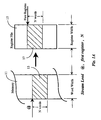
Fig. 3A is an illustration of vector-masks, andFig. 3B illustrates amemory 17 and a register file (context register) 19 wherein bytes frommemory 17 are transferred intofile 19 according to the vector-mask ofFig. 3A . - Referring now to
Fig. 3A , in each submask there are two vectors, being a select vector and a register vector. A submask as illustrated inFig. 3A may be a complete mask, and a complete mask may consist of up to eight (in this embodiment) submasks. This is described in more detail below. - Referring now to
submask 0 inFig. 3A , there are ones inbits - Referring now to
Fig. 3B ,memory 17 is organized as 32 bytes wide. In this example the application is packet processing, and the data entities manipulated are bytes from header fields for packets. As described before, the beginning position for selecting data entities is given in the Masked Load instruction as the first argument @ (for address, seeFig. 2A ). The third argument provides the Mask number, which is, in this case the two-vector submask ofFig. 3A . The relevant bytes of the packet header stored inmemory 17 and indicated as to-be-transferred bysubmask 0 ofFig. 3A are shown inmemory 17 ofFig. 3B as shaded, each a different shading. This any combination or all of the bytes from the packet header of 32 bytes may be selected for transfer to a register file. - The Register vector of
submask 0 indicates the relative position within the register file to write the selected bytes. Note there is a one in only one position in the Register vector in this particular example, that atposition 12. The significance of the one in the register vector is to index the register wherein bytes are to be stored in the register file. There may in other examples be more than a single one in the register vector. - Referring now to
Fig. 3B , bytes are stored in the register file beginning at a first register (FR). The first register for storage (start loading register) is the second argument of the Masked Load instruction. In other applications and embodiments there may be different defaults for different reasons. The Masked Load instruction in this example begins loading selected bytes frommemory 17 intoregister file 19 at the first register and the default is to load in order from the least significant position, and adjacent, until the register is indexed by the register vector. Another order could well be used in another embodiment. Accordinglybytes position 12 in the Register vector ofFig. 3A indexes the register, so bytes 12 and 13 are loaded into the first two positions of register FR+1. As there are no more bytes frommemory 17 selected, this is the end of the operation. - As described above and illustrated herein,
submask 0 is a complete mask. In a preferred embodiment, however, up to eight submasks may be combined to make a mask. Each submask in this embodiment has an end-of-mask bit as indicated inFig. 3B . A one in the end-of-mask bit indicates that submask is the-last submask to be combined to form the mask for a particular instruction. - It is emphasized that the example of vector masks described just above is a single example. Many other masking schemes are possible within the scope of the invention. For example, selection and placement could be indicated by a single vector wherein a first data entity indicated to be selected beginning at a first address would be copied to a first register, and one or more zeros between data entities to be selected would indicate an index in the register in which following entities are to be placed in the register file. Many such schemes are possible, and a relatively few are indicated by example herein.
- It will be apparent to the skilled artisan that, just as described above in the case of Stream Load and Store instructions. Masked Store may be accomplished in much the same fashion as the Masked Load instruction described in detail.
- In the store operations of the example, note that there are bytes of the register file to which data entities are not written. There is a choice of whether to leave these bytes or to clear them. In a preferred embodiment the unused bytes are cleared.
- It will be apparent to the skilled artisan that there are many variations that may be made in the embodiments of the present invention described above without departing from the scope of the invention. For example, there are a wide variety of ways that masks may be structured and implemented, and a wide variety of ways that masks may be stored, programmed, exchanged, and amended. There are similarly a variety of ways Masked Load and Store instructions may be defined and implemented, depending on the Instruction Set Architecture used. There are similarly many applications for such unique instructions beyond the packet-processing applications used as examples herein, and the new instructions may be useful with many kinds of processors, including Dynamic Multi-Streaming (DMS) Processors, which are a particular interest of the present inventors.
- In the matter of DMS processors, the present application is related to four cases teaching aspects of DMS processors and their functioning, all four of which are listed in the Cross-Reference section above. The use of the stream and masked load/store instructions as taught above are especially interesting in DMS processors, since the stream that executes the new instructions in a thread can remain inactive while the masked load/store instruction is being executed in a functional unit. Therefore, other streams can make use of the rest of the resources of the processor. The stream executing the new instructions does not need to sit idle until the masked load/store completes, however. That stream can go on and execute more instructions, as long as the instructions do not depend on the values in the registers affected by the masked load/store instruction in execution. In other words, the stream could execute instructions out-of-order.
- In addition to the above, there is a wide choice of granularity in different embodiments of the invention. In the example used, bytes are selected, but in other embodiments the granularity may be bits, words, or even blocks of memory. If words are used, there need not be a register vector, if the register is of the same word width. It should further be noted that the Stream Load and Store operations are simply a particular case of the Masked Load and Store operations.
Claims (38)
- In computer operation, a method for selecting data entities (13) from a memory (11) and writing the data entities (13) to a register file (15), comprising steps of:consulting a first map of entities to copy relative to a first address;selecting and reading entities indicated by the first map; andconsulting a second map of positions to write the entities copied from the memory (11), relative to a first register; andwriting the entities according to the second map.
- The method of claim 1 wherein the steps follow from a Masked Load instruction implemented according to an instruction set architecture (ISA).
- The method of claim 2 wherein the ISA is MIPS.
- The method of claim 1 wherein said first address, said first register, and a mask number are designated by separate arguments of the single instruction.
- The methods of claim 1 wherein the first and second maps are implemented as bit strings, wherein the position of bits in the string indicate the positions for data entities (13) to be selected from memory (11), and the registers to which data entities (13) are to be written.
- The method of claim 5 wherein bit string maps are expressed as sub-masks, and sub masks are linkable in different combinations to provide combined masks.
- The method of claim 2 wherein the execution of the Masked Load is performed in a Dynamic Multi-streaming (DMS) processor by a first stream running a first thread, and the first stream remains inactive while the Masked Load instruction is executed.
- The method of claim 2 wherein the execution of the Masked Load is performed in a Dynamic Multi-streaming (DMS) processor by a first stream running a first thread, and the first stream executes instructions that do not depend on values in memory (11) affected by the Masked Load instruction while the Masked Load instruction is executed.
- The method of claim 1, further comprising executing a plurality of individual streams in a dynamic multistreaming (DMS) processor, wherein individual masks are dedicated for exclusive use by individual ones of the plurality of individual streams.
- In computer operation, a method for selecting data entities (13) from a register file (15) and writing the data entities (13) to a memory (11), comprising steps of:consulting a first map of entities to read relative to a first register;selecting and reading those the entities indicated by the first map;consulting a second map of positions to write the entities read from the register file (15), relative to a first address; andwriting the entities to the memory according to the second map.
- The method of claim 10 wherein the steps follow from a Masked Store instruction implemented according to an instruction set architecture (ISA).
- The method of claim 11 wherein the ISA is MIPS.
- The method of claim 10 wherein said first address, said first register, and a mask number are designated by separate arguments of the single instruction.
- The method of claim 10 wherein the first and second maps are implemented as bit strings, wherein the position of bits in the string indicate the positions for data entities (13) to be read, and the registers to which data entities (13) are to be written.
- The method of claim 14 wherein bit string maps are expressed as sub-masks, and sub masks are linkable in different combinations to provide combined masks.
- The method of claim 11 wherein the execution of the Masked Store is performed in a Dynamic Multi-streaming (DMS) processor by a first stream running a first thread, and the first stream remains inactive while the Masked Store instruction is executed.
- The method of claim 11 wherein the execution of the Masked Store is performed in a Dynamic Multi-streaming (DMS) processor by a first stream running a first thread, and the first stream executes instruction that do not depend on values in memory affected by the Masked Store instruction while the Masked Store instruction is executed.
- The method of claim 10, further comprising executing a plurality of individual streams in a dynamic multistreaming (DMS) processor, wherein individual masks are dedicated for exclusive use by individual ones of the plurality of individual streams.
- For use in computer operations, a Masked Load instruction comprising:an indication of the instruction;a first argument indicating an address in a memory (11);a second argument indicating a first register in a register file (15); anda third argument indicating a mask number indicating where a first map of a predetermined pattern of positions of data entities (13) to select from the memory (11) relative to the address and a second map of a pre-determined pattern of positions to write in the register file (15) relative to the first register are stored.
- For use in computer operations, a Masked Store instruction comprising:an indication of the instruction;a first argument indicating a first register in a register file (15);a second argument indicating an address in a memory (11); anda third argument indicating a mask number designating where a first map of a predetermined pattern of positions of data entities (13) to select from the register file (15) relative to the first register and a second map of a pre-determined pattern of positions to write in the memory (11) relative to the address are stored.
- A computing system comprising:a CPU;a memory (11); anda register file (15);wherein said CPU is configured to:execute an instruction for loading data entities (13) from the memory (11) into the register file (15); andin executing said instruction, select and read data entities (13) from the memory (11) according to a first map of a pre-determined pattern of positions relative to an address of the memory (11), and write the data entities (13) to the register file (15) according to a second map of a pre-determined pattern of positions relative to a first register of the register file (15).
- The system of claim 21 wherein instruction is a Masked Load instruction implemented according to an instruction set architecture (ISA) and executed by the CPU.
- The system of claim 22 wherein the ISA is MIPS.
- The system of claim 21 wherein said address, said first register, and a mask number indicating where said first map and said second map are stored are designated by separate arguments of the single instruction.
- The system of claim 24 wherein the stored masks are implemented as two bit string vectors, a first vector indicating which data entities (13) relative to the first address to read, and the second indicating into which registers relative to the first register to write the data entities (13).
- The system of claim 25 wherein bit string maps are expressed as sub-masks, and sub masks are linkable in different combinations to provide combined masks.
- The system of claim 22 wherein the execution of the Masked Load is performed in a Dynamic Multi-streaming (DMS) processor by a first stream running a first thread, and the first stream remains inactive while the Stream Load instruction is executed.
- The system of claim 22 wherein the execution of the Masked Load is performed in a Dynamic Multi-streaming (DMS) processor by a first stream running a first thread, and the first stream executes instructions that do not depend on values in memory affected by the Masked Load instruction while the Masked Load instruction is executed.
- The system of claim 21, further comprising executing a plurality of individual streams in a dynamic multistreaming (DMS) processor, wherein individual masks are dedicated for exclusive use by individual ones of the plurality of individual streams.
- A computing system comprising:a CPU;a memory (11); anda register file (15);wherein said CPU is configured to:execute an instruction for storing data entities (13) into the memory (11) from the register file (15); andin executing said instruction, select and read data entities (13) from the register file (15) according to a first map of a pre-determined pattern of positions relative to a first register of the register file (15), and write the data entities (13) to the memory according to a second map of a pre-determined pattern of positions relative to an address of the memory (11).
- The system of claim 30 wherein the instruction is a Masked Store instruction implemented according to an instruction set architecture (ISA) and executed by the CPU.
- The system of claim 31 wherein the ISA is MIPS.
- The system of claim 30 wherein said address, said first register, and a mask number indicating where said first map and said second map are stored are designated by separate arguments of the single instruction.
- The system of claim 33 wherein the stored masks are implemented as two bit string vectors, a first vector indicating which data entities (13) relative to the first register to read, and the second indicating into which registers relative to the first address to write the data entities (13).
- The system of claim 34 wherein bit string maps are expressed as sub-masks, and sub masks are linkable in different combinations to provide combined masks.
- The system of claim 31 wherein the execution of the Masked Store Load is performed in a Dynamic Multi-streaming (DMS) processor by a first stream running a first thread, and the first stream remains inactive while the Stream Load instruction is executed.
- The system of claim 31 wherein the execution of the Masked Store is performed in a Dynamic Multi-streaming (DMS) processor by a firs stream running a first thread, and the first stream executes instructions that do not depend on values in memory affected by the Masked Store instruction while the Masked Store instruction is executed.
- The system of claim 30, further comprising executing a plurality of individual streams in a dynamic multistreaming (DMS) processor, wherein individual masks are dedicated for exclusive use by individual ones of the plurality of individual streams.
Applications Claiming Priority (5)
| Application Number | Priority Date | Filing Date | Title |
|---|---|---|---|
| US17693700P | 2000-01-18 | 2000-01-18 | |
| US176937P | 2000-01-18 | ||
| US62980500A | 2000-07-31 | 2000-07-31 | |
| US629805 | 2000-07-31 | ||
| PCT/US2001/000413 WO2001053934A1 (en) | 2000-01-18 | 2001-01-03 | Method and apparatus for improved computer load and store operations |
Publications (3)
| Publication Number | Publication Date |
|---|---|
| EP1257912A1 EP1257912A1 (en) | 2002-11-20 |
| EP1257912A4 EP1257912A4 (en) | 2006-12-20 |
| EP1257912B1 true EP1257912B1 (en) | 2009-08-19 |
Family
ID=26872769
Family Applications (1)
| Application Number | Title | Priority Date | Filing Date |
|---|---|---|---|
| EP01900915A Expired - Lifetime EP1257912B1 (en) | 2000-01-18 | 2001-01-03 | Method and apparatus for improved computer load and store operations |
Country Status (7)
| Country | Link |
|---|---|
| EP (1) | EP1257912B1 (en) |
| JP (1) | JP3721129B2 (en) |
| AT (1) | ATE440321T1 (en) |
| AU (1) | AU2001226324A1 (en) |
| CA (1) | CA2406679A1 (en) |
| DE (1) | DE60139606D1 (en) |
| WO (1) | WO2001053934A1 (en) |
Families Citing this family (8)
| Publication number | Priority date | Publication date | Assignee | Title |
|---|---|---|---|---|
| US6781589B2 (en) * | 2001-09-06 | 2004-08-24 | Intel Corporation | Apparatus and method for extracting and loading data to/from a buffer |
| US7275148B2 (en) * | 2003-09-08 | 2007-09-25 | Freescale Semiconductor, Inc. | Data processing system using multiple addressing modes for SIMD operations and method thereof |
| US7921263B2 (en) * | 2006-12-22 | 2011-04-05 | Broadcom Corporation | System and method for performing masked store operations in a processor |
| CN102736895B (en) * | 2011-04-07 | 2015-06-10 | 中兴通讯股份有限公司 | Method for realizing data transfer among register files and device |
| KR101949417B1 (en) * | 2011-12-02 | 2019-02-20 | 삼성전자주식회사 | Processor, Apparatus and method for generating instruction |
| US9501276B2 (en) | 2012-12-31 | 2016-11-22 | Intel Corporation | Instructions and logic to vectorize conditional loops |
| US9830151B2 (en) * | 2014-12-23 | 2017-11-28 | Intel Corporation | Method and apparatus for vector index load and store |
| CN113132124B (en) * | 2019-12-30 | 2024-03-19 | 中兴通讯股份有限公司 | Alarm information configuration method, alarm scanning method, device and system |
Family Cites Families (6)
| Publication number | Priority date | Publication date | Assignee | Title |
|---|---|---|---|---|
| JP2616182B2 (en) * | 1990-08-29 | 1997-06-04 | 三菱電機株式会社 | Data processing device |
| JP2665111B2 (en) * | 1992-06-18 | 1997-10-22 | 日本電気株式会社 | Vector processing equipment |
| US5649144A (en) * | 1994-06-13 | 1997-07-15 | Hewlett-Packard Co. | Apparatus, systems and methods for improving data cache hit rates |
| JP2889845B2 (en) * | 1995-09-22 | 1999-05-10 | 松下電器産業株式会社 | Information processing device |
| US5913054A (en) * | 1996-12-16 | 1999-06-15 | International Business Machines Corporation | Method and system for processing a multiple-register instruction that permit multiple data words to be written in a single processor cycle |
| US6119203A (en) * | 1998-08-03 | 2000-09-12 | Motorola, Inc. | Mechanism for sharing data cache resources between data prefetch operations and normal load/store operations in a data processing system |
-
2001
- 2001-01-03 EP EP01900915A patent/EP1257912B1/en not_active Expired - Lifetime
- 2001-01-03 AT AT01900915T patent/ATE440321T1/en not_active IP Right Cessation
- 2001-01-03 DE DE60139606T patent/DE60139606D1/en not_active Expired - Lifetime
- 2001-01-03 JP JP2001554162A patent/JP3721129B2/en not_active Expired - Fee Related
- 2001-01-03 CA CA002406679A patent/CA2406679A1/en not_active Abandoned
- 2001-01-03 WO PCT/US2001/000413 patent/WO2001053934A1/en not_active Ceased
- 2001-01-03 AU AU2001226324A patent/AU2001226324A1/en not_active Abandoned
Also Published As
| Publication number | Publication date |
|---|---|
| JP3721129B2 (en) | 2005-11-30 |
| CA2406679A1 (en) | 2001-07-26 |
| WO2001053934A1 (en) | 2001-07-26 |
| DE60139606D1 (en) | 2009-10-01 |
| ATE440321T1 (en) | 2009-09-15 |
| JP2003521035A (en) | 2003-07-08 |
| EP1257912A4 (en) | 2006-12-20 |
| EP1257912A1 (en) | 2002-11-20 |
| AU2001226324A1 (en) | 2001-07-31 |
Similar Documents
| Publication | Publication Date | Title |
|---|---|---|
| US7529907B2 (en) | Method and apparatus for improved computer load and store operations | |
| US12235773B2 (en) | Two address translations from a single table look-aside buffer read | |
| US11269638B2 (en) | Exposing valid byte lanes as vector predicates to CPU | |
| US5860085A (en) | Instruction set for a content addressable memory array with read/write circuits and an interface register logic block | |
| US6523090B2 (en) | Shared instruction cache for multiple processors | |
| US6128614A (en) | Method of sorting numbers to obtain maxima/minima values with ordering | |
| KR100956970B1 (en) | System and Method for Masked Storage Operations in a Processor | |
| US12061908B2 (en) | Dual data streams sharing dual level two cache access ports to maximize bandwidth utilization | |
| US11934833B2 (en) | Stream data unit with multiple head registers | |
| US6732253B1 (en) | Loop handling for single instruction multiple datapath processor architectures | |
| JPS6217252B2 (en) | ||
| JPH04172533A (en) | Electronic computer | |
| US7308559B2 (en) | Digital signal processor with cascaded SIMD organization | |
| JP2005527035A (en) | Access to wide memory | |
| EP1257912A1 (en) | Method and apparatus for improved computer load and store operations | |
| KR19990036893A (en) | Processor Architecture for Execution of Multiple Addressing Modes and Its Design Method | |
| US7546442B1 (en) | Fixed length memory to memory arithmetic and architecture for direct memory access using fixed length instructions | |
| JP2002529847A (en) | Digital signal processor with bit FIFO | |
| WO2008043287A1 (en) | Configurable single instruction multiple data unit | |
| US6223275B1 (en) | Microprocessor with reduced instruction set limiting the address space to upper 2 Mbytes and executing a long type register branch instruction in three intermediate instructions | |
| KR960016401B1 (en) | Page selecting circuit of register pages using register page pointer | |
| JP2576589B2 (en) | Virtual storage access control method | |
| JP2001166918A (en) | Processor system | |
| JPH0546389A (en) | Parallel processor | |
| JPS62139058A (en) | Memory controller |
Legal Events
| Date | Code | Title | Description |
|---|---|---|---|
| PUAI | Public reference made under article 153(3) epc to a published international application that has entered the european phase |
Free format text: ORIGINAL CODE: 0009012 |
|
| 17P | Request for examination filed |
Effective date: 20020702 |
|
| AK | Designated contracting states |
Kind code of ref document: A1 Designated state(s): AT BE CH CY DE DK ES FI FR GB GR IE IT LI LU MC NL PT SE TR |
|
| AX | Request for extension of the european patent |
Free format text: AL;LT;LV;MK;RO;SI |
|
| RAP1 | Party data changed (applicant data changed or rights of an application transferred) |
Owner name: MIPS TECHNOLOGIES, INC. |
|
| A4 | Supplementary search report drawn up and despatched |
Effective date: 20061121 |
|
| RIC1 | Information provided on ipc code assigned before grant |
Ipc: G06F 9/312 20060101AFI20061115BHEP |
|
| 17Q | First examination report despatched |
Effective date: 20070216 |
|
| GRAP | Despatch of communication of intention to grant a patent |
Free format text: ORIGINAL CODE: EPIDOSNIGR1 |
|
| GRAS | Grant fee paid |
Free format text: ORIGINAL CODE: EPIDOSNIGR3 |
|
| GRAA | (expected) grant |
Free format text: ORIGINAL CODE: 0009210 |
|
| AK | Designated contracting states |
Kind code of ref document: B1 Designated state(s): AT BE CH CY DE DK ES FI FR GB GR IE IT LI LU MC NL PT SE TR |
|
| REG | Reference to a national code |
Ref country code: GB Ref legal event code: FG4D |
|
| REG | Reference to a national code |
Ref country code: CH Ref legal event code: EP |
|
| REG | Reference to a national code |
Ref country code: IE Ref legal event code: FG4D |
|
| REF | Corresponds to: |
Ref document number: 60139606 Country of ref document: DE Date of ref document: 20091001 Kind code of ref document: P |
|
| PG25 | Lapsed in a contracting state [announced via postgrant information from national office to epo] |
Ref country code: FI Free format text: LAPSE BECAUSE OF FAILURE TO SUBMIT A TRANSLATION OF THE DESCRIPTION OR TO PAY THE FEE WITHIN THE PRESCRIBED TIME-LIMIT Effective date: 20090819 Ref country code: AT Free format text: LAPSE BECAUSE OF FAILURE TO SUBMIT A TRANSLATION OF THE DESCRIPTION OR TO PAY THE FEE WITHIN THE PRESCRIBED TIME-LIMIT Effective date: 20090819 Ref country code: ES Free format text: LAPSE BECAUSE OF FAILURE TO SUBMIT A TRANSLATION OF THE DESCRIPTION OR TO PAY THE FEE WITHIN THE PRESCRIBED TIME-LIMIT Effective date: 20091130 Ref country code: SE Free format text: LAPSE BECAUSE OF FAILURE TO SUBMIT A TRANSLATION OF THE DESCRIPTION OR TO PAY THE FEE WITHIN THE PRESCRIBED TIME-LIMIT Effective date: 20090819 |
|
| NLV1 | Nl: lapsed or annulled due to failure to fulfill the requirements of art. 29p and 29m of the patents act | ||
| PG25 | Lapsed in a contracting state [announced via postgrant information from national office to epo] |
Ref country code: NL Free format text: LAPSE BECAUSE OF FAILURE TO SUBMIT A TRANSLATION OF THE DESCRIPTION OR TO PAY THE FEE WITHIN THE PRESCRIBED TIME-LIMIT Effective date: 20090819 |
|
| PG25 | Lapsed in a contracting state [announced via postgrant information from national office to epo] |
Ref country code: PT Free format text: LAPSE BECAUSE OF FAILURE TO SUBMIT A TRANSLATION OF THE DESCRIPTION OR TO PAY THE FEE WITHIN THE PRESCRIBED TIME-LIMIT Effective date: 20091221 Ref country code: CY Free format text: LAPSE BECAUSE OF FAILURE TO SUBMIT A TRANSLATION OF THE DESCRIPTION OR TO PAY THE FEE WITHIN THE PRESCRIBED TIME-LIMIT Effective date: 20090819 |
|
| PG25 | Lapsed in a contracting state [announced via postgrant information from national office to epo] |
Ref country code: DK Free format text: LAPSE BECAUSE OF FAILURE TO SUBMIT A TRANSLATION OF THE DESCRIPTION OR TO PAY THE FEE WITHIN THE PRESCRIBED TIME-LIMIT Effective date: 20090819 |
|
| PLBE | No opposition filed within time limit |
Free format text: ORIGINAL CODE: 0009261 |
|
| STAA | Information on the status of an ep patent application or granted ep patent |
Free format text: STATUS: NO OPPOSITION FILED WITHIN TIME LIMIT |
|
| PG25 | Lapsed in a contracting state [announced via postgrant information from national office to epo] |
Ref country code: BE Free format text: LAPSE BECAUSE OF FAILURE TO SUBMIT A TRANSLATION OF THE DESCRIPTION OR TO PAY THE FEE WITHIN THE PRESCRIBED TIME-LIMIT Effective date: 20090819 |
|
| 26N | No opposition filed |
Effective date: 20100520 |
|
| PG25 | Lapsed in a contracting state [announced via postgrant information from national office to epo] |
Ref country code: MC Free format text: LAPSE BECAUSE OF NON-PAYMENT OF DUE FEES Effective date: 20100131 |
|
| REG | Reference to a national code |
Ref country code: CH Ref legal event code: PL |
|
| PG25 | Lapsed in a contracting state [announced via postgrant information from national office to epo] |
Ref country code: GR Free format text: LAPSE BECAUSE OF FAILURE TO SUBMIT A TRANSLATION OF THE DESCRIPTION OR TO PAY THE FEE WITHIN THE PRESCRIBED TIME-LIMIT Effective date: 20091120 Ref country code: CH Free format text: LAPSE BECAUSE OF NON-PAYMENT OF DUE FEES Effective date: 20100131 Ref country code: LI Free format text: LAPSE BECAUSE OF NON-PAYMENT OF DUE FEES Effective date: 20100131 |
|
| PG25 | Lapsed in a contracting state [announced via postgrant information from national office to epo] |
Ref country code: IE Free format text: LAPSE BECAUSE OF NON-PAYMENT OF DUE FEES Effective date: 20100103 |
|
| PG25 | Lapsed in a contracting state [announced via postgrant information from national office to epo] |
Ref country code: IT Free format text: LAPSE BECAUSE OF FAILURE TO SUBMIT A TRANSLATION OF THE DESCRIPTION OR TO PAY THE FEE WITHIN THE PRESCRIBED TIME-LIMIT Effective date: 20090819 |
|
| PG25 | Lapsed in a contracting state [announced via postgrant information from national office to epo] |
Ref country code: LU Free format text: LAPSE BECAUSE OF NON-PAYMENT OF DUE FEES Effective date: 20100103 |
|
| PG25 | Lapsed in a contracting state [announced via postgrant information from national office to epo] |
Ref country code: TR Free format text: LAPSE BECAUSE OF FAILURE TO SUBMIT A TRANSLATION OF THE DESCRIPTION OR TO PAY THE FEE WITHIN THE PRESCRIBED TIME-LIMIT Effective date: 20090819 |
|
| REG | Reference to a national code |
Ref country code: GB Ref legal event code: 732E Free format text: REGISTERED BETWEEN 20140612 AND 20140618 |
|
| REG | Reference to a national code |
Ref country code: DE Ref legal event code: R082 Ref document number: 60139606 Country of ref document: DE Representative=s name: BENEDUM HASELTINE LAKE PARTNERS, DE Effective date: 20140703 Ref country code: DE Ref legal event code: R081 Ref document number: 60139606 Country of ref document: DE Owner name: ARM FINANCE OVERSEAS LTD., GB Free format text: FORMER OWNER: MIPS TECHNOLOGIES, INC., MOUNTAIN VIEW, CALIF., US Effective date: 20140703 Ref country code: DE Ref legal event code: R082 Ref document number: 60139606 Country of ref document: DE Representative=s name: HASELTINE LAKE LLP, DE Effective date: 20140703 |
|
| REG | Reference to a national code |
Ref country code: DE Ref legal event code: R082 Ref document number: 60139606 Country of ref document: DE Representative=s name: HASELTINE LAKE LLP, DE |
|
| REG | Reference to a national code |
Ref country code: FR Ref legal event code: TP Owner name: ARM FINANCE OVERSEAS LIMITED, GB Effective date: 20150313 Ref country code: FR Ref legal event code: CA Effective date: 20150313 |
|
| REG | Reference to a national code |
Ref country code: FR Ref legal event code: PLFP Year of fee payment: 16 |
|
| REG | Reference to a national code |
Ref country code: FR Ref legal event code: PLFP Year of fee payment: 17 |
|
| REG | Reference to a national code |
Ref country code: FR Ref legal event code: PLFP Year of fee payment: 18 |
|
| PGFP | Annual fee paid to national office [announced via postgrant information from national office to epo] |
Ref country code: FR Payment date: 20181213 Year of fee payment: 19 |
|
| PGFP | Annual fee paid to national office [announced via postgrant information from national office to epo] |
Ref country code: GB Payment date: 20190102 Year of fee payment: 19 Ref country code: DE Payment date: 20181218 Year of fee payment: 19 |
|
| REG | Reference to a national code |
Ref country code: DE Ref legal event code: R119 Ref document number: 60139606 Country of ref document: DE |
|
| GBPC | Gb: european patent ceased through non-payment of renewal fee |
Effective date: 20200103 |
|
| PG25 | Lapsed in a contracting state [announced via postgrant information from national office to epo] |
Ref country code: DE Free format text: LAPSE BECAUSE OF NON-PAYMENT OF DUE FEES Effective date: 20200801 Ref country code: FR Free format text: LAPSE BECAUSE OF NON-PAYMENT OF DUE FEES Effective date: 20200131 Ref country code: GB Free format text: LAPSE BECAUSE OF NON-PAYMENT OF DUE FEES Effective date: 20200103 |