EP1256874A2 - Fast A/D conversion signal processor, and fast A/D conversion device - Google Patents
Fast A/D conversion signal processor, and fast A/D conversion device Download PDFInfo
- Publication number
- EP1256874A2 EP1256874A2 EP02253298A EP02253298A EP1256874A2 EP 1256874 A2 EP1256874 A2 EP 1256874A2 EP 02253298 A EP02253298 A EP 02253298A EP 02253298 A EP02253298 A EP 02253298A EP 1256874 A2 EP1256874 A2 EP 1256874A2
- Authority
- EP
- European Patent Office
- Prior art keywords
- signal
- digital
- clock
- data
- circuit
- Prior art date
- Legal status (The legal status is an assumption and is not a legal conclusion. Google has not performed a legal analysis and makes no representation as to the accuracy of the status listed.)
- Withdrawn
Links
Images


Classifications
-
- G—PHYSICS
- G06—COMPUTING OR CALCULATING; COUNTING
- G06F—ELECTRIC DIGITAL DATA PROCESSING
- G06F5/00—Methods or arrangements for data conversion without changing the order or content of the data handled
- G06F5/06—Methods or arrangements for data conversion without changing the order or content of the data handled for changing the speed of data flow, i.e. speed regularising or timing, e.g. delay lines, FIFO buffers; over- or underrun control therefor
-
- H—ELECTRICITY
- H03—ELECTRONIC CIRCUITRY
- H03M—CODING; DECODING; CODE CONVERSION IN GENERAL
- H03M1/00—Analogue/digital conversion; Digital/analogue conversion
- H03M1/12—Analogue/digital converters
-
- G—PHYSICS
- G01—MEASURING; TESTING
- G01R—MEASURING ELECTRIC VARIABLES; MEASURING MAGNETIC VARIABLES
- G01R33/00—Arrangements or instruments for measuring magnetic variables
- G01R33/20—Arrangements or instruments for measuring magnetic variables involving magnetic resonance
- G01R33/28—Details of apparatus provided for in groups G01R33/44 - G01R33/64
- G01R33/32—Excitation or detection systems, e.g. using radio frequency signals
- G01R33/36—Electrical details, e.g. matching or coupling of the coil to the receiver
- G01R33/3621—NMR receivers or demodulators, e.g. preamplifiers, means for frequency modulation of the MR signal using a digital down converter, means for analog to digital conversion [ADC] or for filtering or processing of the MR signal such as bandpass filtering, resampling, decimation or interpolation
Definitions
- the present invention relates to a fast A/D (Analog to Digital) conversion signal processor, an RF (Radio Frequency) receiver circuit, a digital receiver front end circuit, an MRI (Magnetic Resonance Imaging) apparatus, and a fast A/D conversion device.
- A/D Analog to Digital
- RF Radio Frequency
- MRI Magnetic Resonance Imaging
- the invention relates to a fast A/D conversion signal processor which, even in the presence of discordance in terms of timing between the output of digital data from a fast A/D converter and the clock signal for a digital signal process used by a digital signal process section, can absorb the discordance and deliver the digital data from the fast A/D converter to the digital signal process section properly, an RF receiver circuit and digital receiver front end circuit which can be used for the fast A/D conversion signal processor, an MRI apparatus which uses the fast A/D conversion signal processor, and a fast A/D conversion device which can be used for the fast A/D conversion signal processor.
- an NMR signal received by a receiving coil is converted with a fast A/D converter into digital data, with resulting digital data being delivered to a digital signal process section, which implements a digital signal processing (e.g., digital filtering) for the digital data, with resulting data being delivered to a computer, which implements an image recomposing process or the like.
- a digital signal processing e.g., digital filtering
- This timing discordance is the natural consequence in case the clock signal for the fast A/D converter and the clock signal for the digital signal process are produced independently of each other, and it also emerges when one clock signal is used distributively as both clock signals.
- Conceivable causes are that the clock signal circuit for the fast A/D converter uses an RF pulse transformer for generating differential RF clock signals which are needed by the fast A/D converter, and that there is the disparity in the timing of output of digital data from the fast A/D converter among circuit devices, and that there is a difference between the delay time of a digital data transfer system and the delay time of a clock signal transfer system.
- the present invention seeks to provide a fast A/D conversion signal processor which, even in the presence of discordance in terms of timing between the output of digital data from a fast A/D converter and the clock signal for a digital signal process used by a digital signal process section, can absorb the discordance and deliver the digital data from the fast A/D converter to the digital signal process section properly.
- the present invention further seeks to provide an RF receiver circuit and digital receiver front end circuit which can be used for the fast A/D conversion signal processor.
- the present invention still further seeks to provide an MRI apparatus which uses the fast A/D conversion signal processor.
- the present invention also seeks to provide a fast A/D conversion device which can be used for the fast A/D conversion signal processor.
- a fast A/D conversion signal processor which is characterized by comprising a fast A/D converter which converts an input analog signal into digital data at an operation speed of 20 MHz or higher, a digital signal process section which implements a digital signal processing for the digital data, and data memory means which stores the digital data released by the fast A/D converter in synchronism with a data ready signal provided by the fast A/D converter and reads out the stored digital data and delivers to the digital signal process section in synchronism with a clock signal for a digital signal process used by the digital signal process section.
- digital data is stored in the data memory means at the timing of output of the digital data from the fast A/D converter (at the timing which is based on the data ready signal).
- Digital data is read out of the data memory means and delivered to the digital signal process section at the operation timing of the digital signal process section (at the timing which is based on the clock signal for the digital signal process).
- the discordance is absorbed by the intervention of the data memory means and the digital data can be delivered from the fast A/D converter to the digital signal process section properly.
- the "data ready signal” signifies a “signal indicative of the output period of valid data”, and it may be called “data valid signal”.
- the data memory means includes a dual-clock-synchronous FIFO (First-In-First-Out), a write control circuit which responds to a start signal indicative of the commencement of storing to store the digital data released by the fast A/D converter into the dual-clock-synchronous FIFO in synchronism with the data ready signal, and a readout control circuit which responds to an empty signal provided by the dual-clock-synchronous FIFO to read the digital data out of the dual-clock-synchronous FIFO in synchronism with the clock signal for the digital signal process.
- FIFO First-In-First-Out
- the fast A/D conversion signal processor of this latter arrangement it is possible to write the digital data released by the fast A/D converter into the dual-clock-synchronous FIFO based on the input of the start signal from the outside.
- Digital data is read out of the dual-clock-synchronous FIFO in response to the empty signal which is produced when the digital data is written into the dual-clock-synchronous FIFO, and consequently the digital data can be delivered from the fast A/D converter to the digital signal process section properly.
- the readout control circuit may produce and release a sync ready signal for indicating to the outside that digital data is amid the readout of the dual-clock-synchronous FIFO.
- a high-stability crystal oscillator an RF multiplying circuit which produces an RF clock signal having a frequency that is a multiple of the frequency of the output signal of the high-stability crystal oscillator, and an RF pulse transformer which produces differential RF clock signals to be used by the fast A/D converter from the RF clock signal may be provided.
- the fast A/D conversion signal processor of the foregoing arrangement may comprise a separation RF pulse transformer which produced from the RF clock signal a separated clock signal which is separated electrically from the RF clock signal, and a comparator which produces the clock signal for the digital signal process from the separated clock signal.
- an MRI apparatus may include the fast A/D conversion signal processor of the foregoing arrangement, and being adapted to process with the fast A/D conversion signal processor an NMR signal which is received by a receiving coil.
- an RF receiver circuit comprises a fast A/D converter which converts an input analog signal into digital data at an operation speed of 20 MHz or higher, a high-stability crystal oscillator, an RF multiplying circuit which produces an RF clock signal having a frequency that is a multiple of the frequency of the output signal of the high-stability crystal oscillator, an RF pulse transformer which produces differential RF clock signals to be used by the fast A/D converter from the RF clock signal, a clock driver which delivers to the outside a data ready signal produced by the fast A/D converter, a separation RF pulse transformer which produced from the RF clock signal a separated clock signal which is separated electrically from the RF clock signal, a comparator which produces a clock signal for a digital signal process from the separated clock signal, and a latch which holds and releases in synchronism with the data ready signal the digital data released by the fast A/D converter.
- a digital receiver front end circuit comprises a first clock buffer which produces a data ready signal from a first input clock signal, a second clock buffer which produces from a second input clock signal and releases also to the outside a clock signal for a digital signal process, a latch which holds and releases input digital data in synchronism with the data ready signal, and data memory means which stores the digital data released by the latch in synchronism with the data ready signal and reads out and releases the stored digital data in synchronism with the clock signal for the digital signal process.
- the digital receiver front end circuit of the foregoing arrangement may have data memory means which includes a dual-clock-synchronous FIFO, a write control circuit which responds to a start signal indicative of the commencement of storing to store the input digital data into the dual-clock-synchronous FIFO in synchronism with the data ready signal, and a readout control circuit which responds to an empty signal provided by the dual-clock-synchronous FIFO to read the digital data out of the dual-clock-synchronous FIFO in synchronism with the clock signal for the digital signal process.
- data memory means which includes a dual-clock-synchronous FIFO, a write control circuit which responds to a start signal indicative of the commencement of storing to store the input digital data into the dual-clock-synchronous FIFO in synchronism with the data ready signal, and a readout control circuit which responds to an empty signal provided by the dual-clock-synchronous FIFO to read the digital data out of the dual-clock-synchronous FIFO in synchronism with the clock signal for the digital signal
- the digital receiver front end circuit of the foregoing arrangement may have a readout control circuit produces and may release a sync ready signal for indicating to the outside that digital data is amid the readout of the dual-clock-synchronous FIFO.
- An MRI apparatus may comprise the RF receiver circuit of the foregoing arrangement, the digital receiver front end circuit of the foregoing arrangement, and a digital signal process section, and characterized in that an NMR signal received by a receiving coil is put as input analog signal into the RF receiver circuit, the digital data released by the latch of the RF receiver circuit is put as input digital data into the digital receiver front end circuit, the data ready signal provided by the clock driver of the RF receiver circuit is put as a first input clock signal into the digital receiver front end circuit, the clock signal for the digital signal process provided by the comparator of the RF receiver circuit is put as a second input clock signal into the digital receiver front end circuit, and the digital data released by the dual-clock-synchronous FIFO of the digital receiver front end circuit and the clock signal for the digital signal process provided by the second clock buffer are put into the digital signal process section.
- an MRI apparatus comprises the RF receiver circuit of the foregoing arrangement, the digital receiver front end circuit of the foregoing arrangement, a digital signal process section, and a control logic section which produces the start signal and puts into the digital receiver front end circuit in response to a pulse sequence, and characterized in that an NMR signal received by a receiving coil is put as input analog signal into the RF receiver circuit, the digital data released by the latch of the RF receiver circuit is put as input digital data into the digital receiver front end circuit, the data ready signal provided by the clock driver of the RF receiver circuit is put as a first input clock signal into the digital receiver front end circuit, the clock signal for the digital signal process provided by the comparator of the RF receiver circuit is put as a second input clock signal into the digital receiver front end circuit, the digital data released by the dual-clock-synchronous FIFO of the digital receiver front end circuit and the clock signal for the digital signal process provided by the second clock buffer are put into the digital signal process section, and the clock signal for the digital signal process provided by the second clock
- the present invention resides in an MRI apparatus which is characterized by comprising the RF receiver circuit of the foregoing arrangement, the digital receiver front end circuit of the foregoing arrangement, a digital signal process section, and a control logic section which produces the start signal and puts into the digital receiver front end circuit in response to a pulse sequence, and characterized in that an NMR signal received by a receiving coil is put as input analog signal into the RF receiver circuit, the digital data released by the latch of the RF receiver circuit is put as input digital data into the digital receiver front end circuit, the data ready signal provided by the clock driver of the RF receiver circuit is put as a first input clock signal into the digital receiver front end circuit, the clock signal for the digital signal process provided by the comparator of the RF receiver circuit is put as a second input clock signal into the digital receiver front end circuit, the digital data released by the dual-clock-synchronous FIFO of the digital receiver front end circuit and the clock signal for the digital signal process provided by the second clock buffer are put into the digital signal process section, and the syn
- a fast A/D conversion device which is characterized by comprising a fast A/D converter which converts an input analog signal into digital data at an operation speed of 20 MHz or higher, and data memory means which stores the digital data released by the fast A/D converter in synchronism with a data ready signal provided by the fast A/D converter and reads out the stored digital data in synchronism with a readout clock signal provided from the outside.
- digital data is stored in the data memory means at the timing of output of the digital data from the fast A/D converter.
- Digital data is read out of the data memory means in synchronism with a readout clock signal provided from the outside.
- the data memory means may include a dual-clock-synchronous FIFO, a write control circuit which responds to a start signal provided from the outside to store the digital data released by the fast A/D converter into the dual-clock-synchronous FIFO in synchronism with the data ready signal, and a readout control circuit which responds to an empty signal provided by the dual-clock-synchronous FIFO to read the digital data out of the dual-clock-synchronous FIFO in synchronism with the readout clock signal.
- this fast A/D conversion device of the fifteenth viewpoint it is possible by providing the start signal from the outside to write the digital data released by the fast A/D converter into the dual-clock-synchronous FIFO. Digital data is read out of the dual-clock-synchronous FIFO in response to the empty signal which is produced at the time of writing of the digital data into the dual-clock-synchronous FIFO, and consequently it is possible to deliver properly the digital data from the fast A/D converter to an external circuit which processes the digital data.
- the readout control circuit may produce and releases a sync ready signal for indicating to the outside that digital data is amid the readout of the dual-clock-synchronous FIFO.
- the fast A/D conversion signal processor of this invention even in the presence of discordance in terms of timing between the output of digital data from the fast A/D converter and the clock signal for a digital signal process used by the digital signal process section, it becomes possible to absorb the discordance and deliver the digital data from the fast A/D converter to the digital signal process section properly.
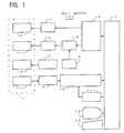
- Fig.1 is a block diagram showing the MRI apparatus 100 based on the first embodiment of this invention.
- a magnet assembly 1 has a room section (bore) in which a subject of inspection is placed, and disposed around the room section are a static magnetic field coil 1p which applies a constant static magnetic field to the subject, a gradient magnetic field coil 1g for generating a gradient magnetic field of the x axis, y axis and z axis (a slice gradient axis, read gradient axis and phase encode gradient axis are formed by the combination of the x axis, y axis and z axis), a transmission coil 1t which produces an RF pulse for inducing the spin of atomic nucleus in the subject, and a reception coil 1r which detects the NMR signal from the subject.
- the static magnetic field coil 1p, gradient magnetic field coil 1g, transmission coil 1t and reception coil 1r are connected to a static magnetic field power source 2, gradient magnetic field drive circuit 3, RF power amplifier 4 and pre-amplifier 5, respectively.
- a permanent magnet may be used in place of the static magnetic field coil 1p and static magnetic field power source 2.
- a sequence memory circuit 6 operates on the gradient magnetic field drive circuit 3 in accordance with the commands from a computer 7 and based on the stored pulse sequence so that the gradient magnetic field coil 1g of the magnet assembly 1 produces a gradient magnetic field and operates on a gate modulation circuit 8 to modulate the carrier output signal of an RF oscillation circuit 9 into a pulse signal having a certain timing and certain envelope, puts the resulting RF pulse into the RF power amplifier 4, and applies the amplified RF pulse to the transmission coil 1t of the magnet assembly 1 so that an intended imaging plane is excited selectively.
- the pre-amplifier 5 amplifies the NMR signal from the subject received by the reception coil 1r of the magnet assembly 1 and puts the amplified signal to a fast A/D conversion signal processor 10.
- the fast A/D conversion signal processor 10 converts the NMR signal into digital data, implements a digital signal processing, and enters the resulting data into computer 7.
- the fast A/D conversion signal processor 10 will be explained in detail later.
- a control logic section 11 controls the operation of the fast A/D conversion signal processor 10 based on the command from the computer 7.
- the computer 7 receives information which is entered from a control console 12.
- the computer 7 reads in digital data from the A/D conversion signal processor 10, and implements the calculation of image reconstruction to produce an MR image.
- the computer 7 also implements general control including the above-mentioned control.
- a display unit 13 displays the MR image.
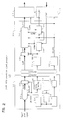
- Fig.2 is a block diagram showing an example of arrangement of the fast A/D conversion signal processor 10.
- the fast A/D conversion signal processor 10 includes an RF receiver circuit 20, a digital receiver front end circuit 30, and a digital signal processing circuit 40.
- the RF receiver circuit 20 is shielded electrically and magnetically against digital circuits including the digital receiver front end circuit 30 and digital signal processing circuit 40 so as to prevent the entry of noises from the digital circuits.
- the RF receiver circuit 20 is arranged to include a fast A/D converter 21 which converts the input NMR signal into digital data D_AD at an operation speed of 20 MHz,40 MHz, etc., a high-stability crystal oscillator 22, an RF multiplying circuit 23 which produces an RF clock signal having a frequency that is a multiple of the frequency of the output signal of the high-stability crystal oscillator 22, an RF pulse transformer 24 for fast A/D converter which produces differential RF clock signals ENC/ENC* to be used by the fast A/D converter from the RF clock signal, a clock driver 25 which inverts and releases to the outside a data ready signal DATA_RDY provided by the fast A/D converter 21, a separation RF pulse transformer 26 which produced from the RF clock signal a separated clock signal which is separated electrically from the RF clock signal, a comparator 27 which produces a clock signal for a digital signal process from the separated clock signal, and a latch 28 which holds the digital data D_AD released by the fast A/D
- Fig.5 shows the timing of the differential RF clock signals ENC/ENC*, digital data D_AD, data ready signal DATA_RDY, and digital data D_RF.
- the digital data D_AD is released at the rising edge of the differential RF clock signal ENC (falling edge of ENC*).
- the data ready signal DATA_RDY is produced at the time when the digital data D_AD settles.
- the digital data D_RF is released at the rising edge of the data ready signal DATA_RDY.
- the digital receiver front end circuit 30 is arranged to include a first clock buffer 31 which produces a data ready signal CLK_AD from the data ready signal DATA_RDY provided by the clock driver 25 of the RF receiver circuit 20, a second clock buffer 32 which produces and releases to the outside a clock signal CLK_DIG for a digital signal process from the clock signal for the digital signal process provided by the comparator 27 of the RF receiver circuit 20, a latch 33 which holds the digital data D_RF provided by the latch 28 of the RF receiver circuit 20 and releases digital data D_DIG in synchronism with the data ready signal CLK_AD, a dual-clock-synchronous FIFO 34 which stores the digital data D_DIG in synchronism with the data ready signal CLK_AD when a write request signal WRREQ becomes "H”, turns an empty signal EMPTY to "L” when it has stored at least one piece of digital data D_DIG, and reads out the stored digital data D_DIG and releases digital data D_FIFO in synchronism
- Fig.3 shows an example of arrangement of the write control circuit 35.
- the write control circuit 35 is made up of two D-type flip-flops 351 and 352 connected in series, and the write request signal WRREQ becomes "H" at the second rise of the clock of the data ready signal CLK_AD after the start signal START indicative of the commencement of storing has become "H".
- Fig.4 shows an example of arrangement of the readout control circuit 36.
- the readout control circuit 36 is made up of an inverting circuit 361, an AND gate 362, and two D-type flip-flops 363 and 364 connected in series, and the read request signal RDREQ and the sync ready signal SYNC_RDY become "H” at the first and second rises, respectively, of the clock signal CLK_DIG for the digital signal process after the write request signal WRREQ has become "H” and the empty signal EMPTY has become "L".
- Fig.5 shows the timing of the data ready signal CLK_AD, clock signal CLK_DIG for the digital signal process, start signal START, write request signal WRREQ, digital data (FIFO) stored in the dual-clock-synchronous FIFO 34, empty signal EMPTY, read request signal RDREQ, digital data D_FIFO released from the dual-clock-synchronous FIFO 34, and sync ready signal SYNC_RDY.
- the digital data D_DIG is released from the latch 33.
- the write request signal WRREQ becomes “H” at the second rise of the data ready signal CLK_AD.
- the dual-clock-synchronous FIFO 34 does not store the digital data D_DIG.
- the dual-clock-synchronous FIFO 34 stores the digital data D_DIG.
- the dual-clock-synchronous FIFO 34 releases the empty signal EMPTY of "H” when it does not store the digital data D_DIG, and it turns the empty signal EMPTY to "L” when it store at least one piece of digital data D_DIG.
- the read request signal RDREQ becomes “H” at the first rise of the clock signal CLK_DIG for the digital signal process after the write request signal WRREQ has become “H” and the empty signal EMPTY has become “L”.
- the dual-clock-synchronous FIFO 34 releases the digital data D_FIFO in synchronism with the rise of the clock signal CLK_DIG for the digital signal process.
- the sync ready signal SYNC_RDY becomes "H” at the second rise of the clock signal CLK_DIG for the digital signal process after the read request signal RDREQ has become “H”.
- the digital signal process section 40 operates based on the clock signal CLK_DIG for the digital signal process to read in the digital data D_FIFO and implement the digital signal process such as digital demodulation (digital orthogonal detection) and digital filtering, and thereafter it delivers resulting data to the computer 7.
- the control logic section 11 operates based on the clock signal CLK_DIG for the digital signal process to turn the start signal START to "H” or "L” in accordance with the command from the computer 7. It also initiates the operation of the digital signal process section 40 after the sync ready signal SYNC_RDY has become “H”.
- the computer 7 issues a command of turning the start signal START to "L” at the time of power-on, issues a command of turning the start signal START to "H” at the timing slightly before the commencement of data collection, and issues a command of turning the start signal START to "L” on completion of data collection.
- the fast A/D conversion signal processor 10 described above, even in the presence of discordance in terms of timing between the output of digital data D_AD from the fast A/D converter 21 and the clock signal CLK_DIG for a digital signal process used by the digital signal process section 40, it is possible to deliver the digital data D_AD from the fast A/D converter 21 to the digital signal process section 40 properly by absorbing the discordance with the dual-clock-synchronous FIFO 34. Based on the easy switching of the operation clock frequency, it is applicable to MRI apparatus of arbitrary magnetic field strength such as 0.2T-1.5T,3T and 4T.
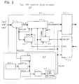
- Fig. 6 is a block diagram showing another example of arrangement of the fast A/D conversion signal processor 10.
- This fast A/D conversion signal processor 10 is arranged to include a fast A/D conversion device 50, a clock circuit 60 and a digital signal processing circuit 40 which are formed in an LSI (Large Scale Integration) device.
- LSI Large Scale Integration
- the fast A/D conversion device 50 is arranged to include a fast A/D converter 21 which converts an input NMR signal into digital data D_AD at an operation speed of 20 MHz,40 MHz, etc., a dual-clock-synchronous FIFO 34 which stores the digital data D_DIG in synchronism with a data ready signal CLK_AD when a write request signal WRREQ becomes "H", turns an empty signal EMPTY to "L” when it has stored at least one piece of digital data D_DIG, and reads out the stored digital data D_DIG and releases digital data D_FIFO in synchronism with a clock signal CLK_DIG for a digital signal process when a read request signal RDREQ becomes "H”, a write control circuit 35 which responds to a start signal START provided by a control logic section 11 to turn the write request signal WRREQ to "H” in synchronism with the data ready signal CLK_AD, and a readout control circuit 36 which responds to the empty signal EMPTY provided the dual-
- the clock circuit 60 is arranged to include a high-stability crystal oscillator 22, an RF multiplying circuit 23 which produces an RF clock signal having a frequency that is a multiple of the frequency of the output signal of the high-stability crystal oscillator 22, an RF pulse transformer 24 for fast A/D converter which produces differential RF clock signals ENC/ENC* to be used by the fast A/D converter from the RF clock signal, a separation RF pulse transformer 26 which produces from the RF clock signal a separated clock signal which is separated electrically from the RF clock signal, a comparator 27 which produces a clock signal for a digital signal process from the separated clock signal, and a clock buffer 32 which produces a clock signal CLK_DIG for the digital signal process from the clock signal for the digital signal process provided by the comparator 27.
- the fast A/D conversion signal processor 10 described above also, the virtually same operation and effectiveness as the first embodiment can be achieved. Owing to the LSI-designed fast A/D conversion device 50, the number of component parts can be smaller.
- the LSI of fast A/D conversion device 50 which releases parallel digital data at a high speed, can be used in combination with a DSP (Digital Signal Processor), etc. for other purposes (e.g., a software wireless communication unit which supports the high quality and high dynamic range communication).
- DSP Digital Signal Processor
- a PLL (Phase Locked Loop) synthesizer circuit may be used in place of the RF multiplying circuit 23.
- the start signal START may be turned to "H” by use of a power-on reset signal.
- Part or whole of the circuit may be formed of programmable devices such as a CPLD (Complex Programmable Logic Device) and FPGA (Field-Programmable Logic Array).
- CPLD Complex Programmable Logic Device
- FPGA Field-Programmable Logic Array
Landscapes
- Physics & Mathematics (AREA)
- Engineering & Computer Science (AREA)
- Theoretical Computer Science (AREA)
- General Physics & Mathematics (AREA)
- Condensed Matter Physics & Semiconductors (AREA)
- General Engineering & Computer Science (AREA)
- Magnetic Resonance Imaging Apparatus (AREA)
- Analogue/Digital Conversion (AREA)
Abstract
Description
Claims (10)
- A fast A/D conversion signal processor comprising:a fast A/D converter which converts an input analog signal into digital data at an operation speed of 20 MHz or higher;a digital signal process section which implements a digital signal process for the digital data; anda data memory device which stores the digital data released by said fast A/D converter in synchronism with a data ready signal provided by said fast A/D converter and reads out the stored digital data and delivers to said digital signal process section in synchronism with a clock signal for the digital signal process used by said digital signal process section.
- The fast A/D conversion signal processor of claim 1, wherein said data memory device includes a dual-clock-synchronous FIFO, a write control circuit which responds to a start signal indicative of the commencement of storing to store the digital data released by said fast A/D converter into said dual-clock-synchronous FIFO in synchronism with the data ready signal, and a readout control circuit which responds to an empty signal provided by said dual-clock-synchronous FIFO to read the digital data out of said dual-clock-synchronous FIFO in synchronism with the clock signal for the digital signal process.
- An RF receiver circuit comprising:a fast A/D converter which converts an input analog signal into digital data at an operation speed of 20 MHz or higher;a high-stability crystal oscillator;an RF multiplying circuit which produces an RF clock signal having a frequency that is a multiple of the frequency of the output signal of said high-stability crystal oscillator;an RF pulse transformer which produces differential RF clock signals to be used by said fast A/D converter from the RF clock signal;a clock driver which delivers to the outside a data ready signal produced by said fast A/D converter;a separation RF pulse transformer which produced from the RF clock signal a separated clock signal which is separated electrically from the RF clock signal;a comparator which produces a clock signal for a digital signal process from the separated clock signal; anda latch which holds and releases in synchronism with the data ready signal the digital data released by said fast A/D converter.
- A digital receiver front end circuit comprising:a first clock buffer which produces a data ready signal from a first input clock signal;a second clock buffer which produces from a second input clock signal and releases also to the outside a clock signal for a digital signal process;a latch which holds and releases input digital data in synchronism with the data ready signal; anda data memory device which stores the digital data released by said latch in synchronism with the data ready signal and reads out and releases the stored digital data in synchronism with the clock signal for the digital signal process.
- The digital receiver front end circuit of claim 4, wherein said data memory device includes a dual-clock-synchronous FIFO, a write control circuit which responds to a start signal indicative of the commencement of storing to store the input digital data into said dual-clock-synchronous FIFO in synchronism with the data ready signal, and a readout control circuit which responds to an empty signal provided by said dual-clock-synchronous FIFO to read the digital data out of said dual-clock-synchronous FIFO in synchronism with the clock signal for the digital signal process.
- The digital receiver front end circuit of claim 5, wherein said readout control circuit produces and releases a sync ready signal for indicating to the outside that digital data is amid the readout of said dual-clock-synchronous FIFO.
- An MRI apparatus comprising: the RF receiver circuit of claim 3; the digital receiver front end circuit of claim 4; and a digital signal process section; and wherein an NMR signal received by a receiving coil is put as input analog signal into said RF receiver circuit, the digital data released by the latch of said RF receiver circuit is put as input digital data into said digital receiver front end circuit, the data ready signal provided the clock driver of said RF receiver circuit is put as a first input clock signal into said digital receiver front end circuit, the clock signal for the digital signal process provided by the comparator of said RF receiver circuit is put as a second input clock signal into said digital receiver front end circuit, and the digital data released by the dual-clock-synchronous FIFO of said digital receiver front end circuit and the clock signal for the digital signal process provided by said second clock buffer are put into said digital signal process section.
- An MRI apparatus comprising: the RF receiver circuit of claim 4; the digital receiver front end circuit of claim 6 or claim 7; a digital signal process section; and a control logic section which produces and puts the start signal into said digital receiver front end circuit in response to a pulse sequence; and wherein an NMR signal received by a receiving coil is put as input analog signal into said RF receiver circuit, the digital data released by the latch of said RF receiver circuit is put as input digital data into said digital receiver front end circuit, the data ready signal provided by the clock driver of said RF receiver circuit is put as a first input clock signal into said digital receiver front end circuit, the clock signal for the digital signal process provided by the comparator of said RF receiver circuit is put as a second input clock signal into said digital receiver front end circuit, the digital data released by the dual-clock-synchronous FIFO of said digital receiver front end circuit and the clock signal for the digital signal process provided by said second clock buffer are put into said digital signal process section, and the clock signal for the digital signal process provided by the second clock buffer of said digital receiver front end circuit is put into said control logic section.
- An MRI apparatus comprising: the RF receiver circuit of claim 3; the digital receiver front end circuit of claim 7; a digital signal process section; and a control logic section which produces and puts the start signal into said digital receiver front end circuit in response to a pulse sequence; and wherein an NMR signal received by a receiving coil is put as input analog signal into said RF receiver circuit, the digital data released by the latch of said RF receiver circuit is put as input digital data into said digital receiver front end circuit, the data ready signal provided by the clock driver of said RF receiver circuit is put as a first input clock signal into said digital receiver front end circuit, the clock signal for the digital signal process provided by the comparator of said RF receiver circuit is put as a second input clock signal into said digital receiver front end circuit, the digital data released by the dual-clock-synchronous FIFO of said digital receiver front end circuit and the clock signal for the digital signal process provided by said second clock buffer are put into said digital signal process section, and the sync ready signal provided by the readout control circuit of said digital receiver front end circuit and the clock signal for the digital signal process provided by the second clock buffer are put into said control logic section.
- A fast A/D conversion device comprising:a fast A/D converter which converts an input analog signal into digital data at an operation speed of 20 MHz or higher; anda data memory device which stores the digital data released by said fast A/D converter in synchronism with a data ready signal provided by said fast A/D converter and reads out the stored digital data in synchronism with a readout clock signal provided from the outside.
Applications Claiming Priority (2)
| Application Number | Priority Date | Filing Date | Title |
|---|---|---|---|
| JP2001141186A JP4369074B2 (en) | 2001-05-11 | 2001-05-11 | High-speed AD conversion signal processing apparatus, digital receiver front-end circuit, and MRI apparatus |
| JP2001141186 | 2001-05-11 |
Publications (2)
| Publication Number | Publication Date |
|---|---|
| EP1256874A2 true EP1256874A2 (en) | 2002-11-13 |
| EP1256874A3 EP1256874A3 (en) | 2006-03-15 |
Family
ID=18987674
Family Applications (1)
| Application Number | Title | Priority Date | Filing Date |
|---|---|---|---|
| EP02253298A Withdrawn EP1256874A3 (en) | 2001-05-11 | 2002-05-10 | Fast A/D conversion signal processor, and fast A/D conversion device |
Country Status (5)
| Country | Link |
|---|---|
| US (1) | US6624777B2 (en) |
| EP (1) | EP1256874A3 (en) |
| JP (1) | JP4369074B2 (en) |
| KR (1) | KR100488861B1 (en) |
| CN (1) | CN1274086C (en) |
Families Citing this family (20)
| Publication number | Priority date | Publication date | Assignee | Title |
|---|---|---|---|---|
| EP1771745A1 (en) * | 2004-07-15 | 2007-04-11 | Koninklijke Philips Electronics N.V. | Wireless mr receiving coil system |
| EP1825287A2 (en) * | 2004-12-06 | 2007-08-29 | Koninklijke Philips Electronics N.V. | Frequency domain multiplexed transmission of mr signals from a receiver coil array |
| US7170433B1 (en) * | 2005-06-20 | 2007-01-30 | The Mathworks, Inc. | Analog I/O board providing analog-to-digital conversion and having a two-level buffer that allows demand based access to converted data |
| JP4629542B2 (en) * | 2005-09-27 | 2011-02-09 | ジーイー・メディカル・システムズ・グローバル・テクノロジー・カンパニー・エルエルシー | Sudden noise removal device |
| US7885630B2 (en) * | 2005-11-30 | 2011-02-08 | Research In Motion Limited | Mobile wireless communications device having buffered clock distribution network for microprocessor and RF circuits |
| US7807474B2 (en) * | 2006-03-24 | 2010-10-05 | Mcw Research Foundation, Inc. | System and method for direct digitization of NMR signals |
| JP4347865B2 (en) | 2006-06-22 | 2009-10-21 | ジーイー・メディカル・システムズ・グローバル・テクノロジー・カンパニー・エルエルシー | Magnetic resonance imaging apparatus and A / D conversion apparatus |
| US8049505B2 (en) * | 2006-12-19 | 2011-11-01 | Koninlijke Philips Electronics N.V. | MRI system with direct digital receiver using resampling |
| ATE508373T1 (en) * | 2007-12-11 | 2011-05-15 | Koninkl Philips Electronics Nv | IMPROVED CLOCK GENERATION IN MRI RECEIVERS |
| JP2011209923A (en) * | 2010-03-29 | 2011-10-20 | Keihin Corp | Control device |
| JP5951931B2 (en) * | 2011-02-25 | 2016-07-13 | ジーイー・メディカル・システムズ・グローバル・テクノロジー・カンパニー・エルエルシー | Signal processing apparatus and magnetic resonance imaging apparatus |
| JP5716584B2 (en) * | 2011-07-06 | 2015-05-13 | 株式会社島津製作所 | X-ray detector |
| US8482444B1 (en) | 2011-07-28 | 2013-07-09 | The Boeing Company | Calibration of analog-to-digital converter data capture |
| JP6112786B2 (en) * | 2012-06-15 | 2017-04-12 | 三菱電機株式会社 | In-reactor neutron flux detector position detector |
| JP6162514B2 (en) | 2013-07-12 | 2017-07-12 | 東芝メディカルシステムズ株式会社 | Magnetic resonance imaging system |
| JP6320746B2 (en) * | 2013-12-25 | 2018-05-09 | キヤノンメディカルシステムズ株式会社 | Magnetic resonance imaging system |
| DE102014211137A1 (en) * | 2014-06-11 | 2015-12-17 | Siemens Aktiengesellschaft | magnetic resonance device |
| JP6632266B2 (en) | 2015-09-04 | 2020-01-22 | キヤノン株式会社 | Imaging device |
| CN106646296B (en) * | 2016-09-30 | 2019-11-19 | 上海联影医疗科技有限公司 | Magnetic resonance reception link and method of reseptance |
| CN109900696B (en) * | 2019-01-25 | 2021-06-01 | 浙江理工大学 | A bag detection method based on dynamic FIFO data processing |
Family Cites Families (22)
| Publication number | Priority date | Publication date | Assignee | Title |
|---|---|---|---|---|
| US4532637A (en) * | 1983-01-03 | 1985-07-30 | Sperry Corporation | Differential receiver |
| US4839652A (en) * | 1987-06-01 | 1989-06-13 | General Electric Company | Method and apparatus for high speed digital phased array coherent imaging system |
| US5022395A (en) * | 1989-07-07 | 1991-06-11 | Cardiac Pacemakers, Inc. | Implantable cardiac device with dual clock control of microprocessor |
| US5227728A (en) | 1991-11-01 | 1993-07-13 | The Regents Of The University Of California | Gradient driver control in magnetic resonance imaging |
| US5442290A (en) | 1992-08-04 | 1995-08-15 | The Regents Of The University Of California | MRI gradient drive current control using all digital controller |
| JPH07171152A (en) * | 1993-12-17 | 1995-07-11 | Olympus Optical Co Ltd | Ultrasonic diagnostic device |
| US5529068A (en) * | 1994-06-16 | 1996-06-25 | The Regents Of The University Of California | Synchronized digital signal processor for MRI reception |
| US5436600A (en) * | 1994-07-29 | 1995-07-25 | The Regents Of The University Of California | MRI multi-frequency DSB and SSB RF synthesizer |
| JPH08146014A (en) * | 1994-11-18 | 1996-06-07 | Olympus Optical Co Ltd | Scanning type probe microscope |
| US5739691A (en) | 1995-11-28 | 1998-04-14 | The Regents Of The University Of California | Multi-frequency digital low pass filter for magnetic resonance imaging |
| US5627482A (en) * | 1996-02-07 | 1997-05-06 | Ceridian Corporation | Electronic digital clock distribution system |
| US6043659A (en) * | 1997-10-31 | 2000-03-28 | General Electric Company | Magnetic resonance imaging system with non-linear preamplification |
| US6226698B1 (en) * | 1997-11-10 | 2001-05-01 | Sun Microsystems, Inc. | Method and apparatus for dynamically calculating degrees of fullness of a synchronous FIFO |
| US6201393B1 (en) | 1997-12-15 | 2001-03-13 | General Electric Company | Reducing image artifacts caused by patient motion during MR imaging |
| JP2000091936A (en) * | 1998-09-14 | 2000-03-31 | Nec Corp | Radio receiver |
| US6459265B1 (en) | 1998-11-25 | 2002-10-01 | General Electric Company | Method and apparatus for reducing input impedance of a preamplifier |
| US6281681B1 (en) | 1999-01-28 | 2001-08-28 | General Electric Company | Magnetic resonance imaging with interleaved Fibonacci spiral scanning |
| US6452391B1 (en) | 1999-06-11 | 2002-09-17 | General Electric Company | Quiet mode magnetic resonance imaging system and method |
| US6242916B1 (en) | 1999-11-17 | 2001-06-05 | General Electric Company | Partial fourier acquistion of MR data over a limited field of view and image reconstruction |
| US6356780B1 (en) | 1999-12-22 | 2002-03-12 | General Electric Company | Method and apparatus for managing peripheral devices in a medical imaging system |
| US6462544B1 (en) | 2000-10-24 | 2002-10-08 | General Electric Company | Magnetic resonance imaging apparatus |
| US6445328B1 (en) * | 2001-03-22 | 2002-09-03 | The United States Of America As Represented By The Secretary Of The Army | Large dynamic range digitizing apparatus and method |
-
2001
- 2001-05-11 JP JP2001141186A patent/JP4369074B2/en not_active Expired - Fee Related
-
2002
- 2002-05-10 US US10/143,168 patent/US6624777B2/en not_active Expired - Fee Related
- 2002-05-10 KR KR10-2002-0025730A patent/KR100488861B1/en not_active Expired - Fee Related
- 2002-05-10 EP EP02253298A patent/EP1256874A3/en not_active Withdrawn
- 2002-05-13 CN CNB021199752A patent/CN1274086C/en not_active Expired - Fee Related
Also Published As
| Publication number | Publication date |
|---|---|
| US20020167434A1 (en) | 2002-11-14 |
| CN1385135A (en) | 2002-12-18 |
| KR20020086284A (en) | 2002-11-18 |
| US6624777B2 (en) | 2003-09-23 |
| KR100488861B1 (en) | 2005-05-11 |
| EP1256874A3 (en) | 2006-03-15 |
| JP4369074B2 (en) | 2009-11-18 |
| CN1274086C (en) | 2006-09-06 |
| JP2002353812A (en) | 2002-12-06 |
Similar Documents
| Publication | Publication Date | Title |
|---|---|---|
| US6624777B2 (en) | Fast A/D conversion signal processor, RF receiver circuit, digital receiver front end circuit, MRI apparatus, and fast A/D conversion device | |
| US5384536A (en) | Nuclear magnetic resonanace inspection apparatus and its method | |
| CN103123386B (en) | For equipment and the method for synchronous clock between the device of magnetic resonance imaging system | |
| CN101563623B (en) | MRI system with direct digital receiver using resampling | |
| US9417300B2 (en) | Direct digital receiver with local free running clock | |
| EP1207402A2 (en) | Magnetic field variation measuring method and magnetic field varation compensating method for MRI apparatus, and MRI apparatus | |
| US7818359B2 (en) | Direct digital synthesizer, direct digital synthesizer for transmission and detection, and MRI apparatus | |
| WO2002097465A2 (en) | Mr data acquisition method, mr image display method and mri apparatus | |
| Hashimoto et al. | Comparison of analog and digital transceiver systems for MR imaging | |
| US20060066312A1 (en) | Magnetic resonance detector and method | |
| JP2001187040A (en) | Method and apparatus for reducing image artifacts caused by magnet vibration in a magnetic resonance imaging system | |
| KR100868118B1 (en) | Rf pulse applying method and mri apparatus | |
| US20070052415A1 (en) | Rf pulse applying method and mri apparatus | |
| NL1033062C2 (en) | RF pulse applying method and MRI equipment. | |
| US7576541B2 (en) | RF coil for MRI apparatus, method of using RF coil for MRI apparatus, and MRI apparatus | |
| KR101967243B1 (en) | Method and apparatus for high-speed magnetic resonance imaging | |
| US4775835A (en) | Magnetic resonance imaging apparatus including sequence controller | |
| JP2007068798A (en) | Rf pulse applying method and mri apparatus | |
| US20240159846A1 (en) | Wireless magnetic resonance imaging (mri) coil with coil functionality that is not reliant on coil control signals from the mri scanner | |
| JP7835611B2 (en) | Magnetic resonance imaging apparatus and control method for magnetic resonance imaging apparatus | |
| JPH04294504A (en) | Magnetic resonance imaging device | |
| JP3341913B2 (en) | MR device | |
| JPH10277002A (en) | Mr continuous image pickup method and mri device | |
| JPH01293856A (en) | Magnetic resonance imaging method | |
| EP0283058A1 (en) | Method and arrangement for suppressing coherent interference effects in magnetic resonance signals |
Legal Events
| Date | Code | Title | Description |
|---|---|---|---|
| PUAI | Public reference made under article 153(3) epc to a published international application that has entered the european phase |
Free format text: ORIGINAL CODE: 0009012 |
|
| AK | Designated contracting states |
Kind code of ref document: A2 Designated state(s): AT BE CH CY DE DK ES FI FR GB GR IE IT LI LU MC NL PT SE TR |
|
| AX | Request for extension of the european patent |
Free format text: AL;LT;LV;MK;RO;SI |
|
| RIN1 | Information on inventor provided before grant (corrected) |
Inventor name: MIYANO, HIROYUKI, GE YOKOGAWA MEDICAL SYSTEMS |
|
| PUAL | Search report despatched |
Free format text: ORIGINAL CODE: 0009013 |
|
| AK | Designated contracting states |
Kind code of ref document: A3 Designated state(s): AT BE CH CY DE DK ES FI FR GB GR IE IT LI LU MC NL PT SE TR |
|
| AX | Request for extension of the european patent |
Extension state: AL LT LV MK RO SI |
|
| 17P | Request for examination filed |
Effective date: 20060915 |
|
| AKX | Designation fees paid |
Designated state(s): DE FR GB |
|
| 17Q | First examination report despatched |
Effective date: 20070420 |
|
| STAA | Information on the status of an ep patent application or granted ep patent |
Free format text: STATUS: THE APPLICATION IS DEEMED TO BE WITHDRAWN |
|
| 18D | Application deemed to be withdrawn |
Effective date: 20081204 |