EP1256004B1 - Spannungssensor - Google Patents
Spannungssensor Download PDFInfo
- Publication number
- EP1256004B1 EP1256004B1 EP01902210A EP01902210A EP1256004B1 EP 1256004 B1 EP1256004 B1 EP 1256004B1 EP 01902210 A EP01902210 A EP 01902210A EP 01902210 A EP01902210 A EP 01902210A EP 1256004 B1 EP1256004 B1 EP 1256004B1
- Authority
- EP
- European Patent Office
- Prior art keywords
- electric field
- isolating
- isolating section
- section
- voltage
- Prior art date
- Legal status (The legal status is an assumption and is not a legal conclusion. Google has not performed a legal analysis and makes no representation as to the accuracy of the status listed.)
- Expired - Lifetime
Links
Images

Classifications
-
- G—PHYSICS
- G01—MEASURING; TESTING
- G01R—MEASURING ELECTRIC VARIABLES; MEASURING MAGNETIC VARIABLES
- G01R15/00—Details of measuring arrangements of the types provided for in groups G01R17/00 - G01R29/00, G01R33/00 - G01R33/26 or G01R35/00
- G01R15/14—Adaptations providing voltage or current isolation, e.g. for high-voltage or high-current networks
- G01R15/144—Measuring arrangements for voltage not covered by other subgroups of G01R15/14
-
- G—PHYSICS
- G01—MEASURING; TESTING
- G01R—MEASURING ELECTRIC VARIABLES; MEASURING MAGNETIC VARIABLES
- G01R1/00—Details of instruments or arrangements of the types included in groups G01R5/00 - G01R13/00 and G01R31/00
- G01R1/02—General constructional details
- G01R1/18—Screening arrangements against electric or magnetic fields, e.g. against earth's field
-
- G—PHYSICS
- G01—MEASURING; TESTING
- G01R—MEASURING ELECTRIC VARIABLES; MEASURING MAGNETIC VARIABLES
- G01R15/00—Details of measuring arrangements of the types provided for in groups G01R17/00 - G01R29/00, G01R33/00 - G01R33/26 or G01R35/00
- G01R15/14—Adaptations providing voltage or current isolation, e.g. for high-voltage or high-current networks
- G01R15/24—Adaptations providing voltage or current isolation, e.g. for high-voltage or high-current networks using light-modulating devices
- G01R15/247—Details of the circuitry or construction of devices covered by G01R15/241 - G01R15/246
-
- G—PHYSICS
- G01—MEASURING; TESTING
- G01R—MEASURING ELECTRIC VARIABLES; MEASURING MAGNETIC VARIABLES
- G01R19/00—Arrangements for measuring currents or voltages or for indicating presence or sign thereof
- G01R19/0046—Arrangements for measuring currents or voltages or for indicating presence or sign thereof characterised by a specific application or detail not covered by any other subgroup of G01R19/00
- G01R19/0053—Noise discrimination; Analog sampling; Measuring transients
Definitions
- the present invention relates to a voltage sensor for measuring voltage and is particularly suitable for measuring high voltages such as on high-voltage power transmission lines.
- the list of known high-voltage voltage sensors includes inductive transformers, capacitive dividers or capacitive voltage transformers, and transducers using bulk-optic electric field sensors.
- the first two sensors suffer from bandwidth restrictions, expensive failure, extensive maintenance, heavy weight, and output variations. They also suffer from the need for substantial insulation that is both expensive and potentially hazardous to the environment (e.g. oil and/or SF 6 gas).
- Pockels cells are known devices that have been used for measuring voltage particularly high voltage, for example see US patent 5477134 issued to H. Hamada and US patent 5731579 issued to G.K. Woods.
- a preferred form of Pockels cell for use in the present invention is an integrated optics Pockels cell such as that described in US patent 5,029,273 issued July 2, 1991 to Jaeger.
- US patent 5,917,316 “Measuring device for a metal-enclosed, gas-insulated high-voltage installation,” issued June 29, 1999, to A Bosco, T. Hertig, and A Kaczkowski, describes a high-voltage voltage sensor that uses a metallic enclosure providing shielding of a voltage detector located inside the enclosure against external voltage sources in order to obtain high measurement accuracy.
- the enclosure contains a high-voltage conductor and is filled with pressurized SF 6 gas in order to sustain high-electric field stresses.
- VTs voltage transducers
- EFS electric field sensor
- AS admittance shielding
- These known admittance shielding systems are conceived by manipulating metallic conductor (electrode) geometries (or as above indicated selecting materials with relatively large permittivities (as taught in the said Jaeger et al. application)) to attain a good level of admittance shielding.
- one method of obtaining AS is to in effect decrease the distance between the two conductors between which voltage is to be measured. Another is to surround one conductor with the other conductor as much as possible. Both of these methods have the effect of increasing the admittance between the two conductors where the EFSs are located. Use of these methods results in the existence of high electric field stresses that must be supported with special insulation such as SF 6 gas. Examples of this can be found in US Patent 3,938,039 "Voltage measuring device for encapsulated high-voltage installations," issued February 10, 1976, to W. Hermstein, G. Rosenberger, and W. Muller; US Patent 5,272,460 “Current and voltage transformer for a metal-encapsulated, gas-insulated high-voltage installation," issued December 21, 1993, to R.
- the present invention reduces significantly the deficiencies inherent to the existing high-voltage sensor technology.
- the simple structure of the invention substantially removes the need for usually expensive and/or environmentally unfriendly insulation; may be made lighter, allowing for less expensive transportation, installation, and maintenance; and is compatible with existing standoff structures, allowing for easy construction.
- the invention When used with compact electric field sensor technology, such as the integrated optics Pockels cell, the invention offers wide bandwidth and easy interfacing with emerging digital technology.
- the present invention provides an apparatus for measuring voltage according to claim 1 and a corresponding method according to claim 21.
- the apparatus for measuring voltage comprises an electrically isolating-section, a pair of spaced conductors between which voltage difference V is to be determined, one of said conductors being at one end of said isolating-section and another at an end of said isolating-section remote from said one end, at least one electric field sensor which senses electric field at at least one location within said isolating-section, a detector for determining a value V d for said voltage difference V based on said electric field(s) sensed by said at least one electric field sensor, said isolating-section formed of a primarily resistive material having a resistance in the range of 25 G ⁇ to 50 k ⁇ so as to provide sufficient shielding of said at least one location from sources of electric field interference of practical strength external to said apparatus so that said sources of practical strength do not change said sensed electric field sensed at said at least one location to generate a significant error in said value V d for said voltage difference V.
- the apparatus for measuring voltage comprises an electrically isolating-section, a pair of spaced conductors between which voltage difference V is to be determined, one of said conductors being at one end of said isolating-section and another at an end of said isolating-section remote from said one end, at least one electric field sensor which senses electric field at at least one location within said isolating-section, a detector for determining a value V d for said voltage difference V based on said electric field sensed by said at least one electric field sensor, said isolating-section formed of a primarily resistive material having a resistance per unit of length in the range of 25 G ⁇ /m to 50 k ⁇ /m so as to provide sufficient shielding of said at least one location from sources of electric field disturbance of practical strength external to said apparatus so that said sources of practical strength do not change said sensed electric field sensed at said at least one location to generate a significant error in said value V d for said voltage difference V.
- said resistance per unit of length is in the range of 1 G ⁇ /m to 500 k ⁇ /m.
- said sufficient shielding reduces the error in said determined voltage V d to less than 25% of an error in V d that would be attained if said isolating-section was not provided.
- said sufficient shielding reduces the error in said determined voltage V d to less than 1%.
- said sufficient shielding reduces the error in said determined voltage V d to less than 0.3%.
- said isolating-section is a hollow section in which the electric field sensor is mounted.
- the material of the isolating-section is polyethylene doped with carbon black.
- the isolating-section is enclosed in a protective sleeve protecting said isolating-section from the environment.
- the electric field sensor is an optical electric field sensor.
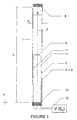
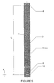
- FIG 1 illustrates the basic structure of the invention.
- FIG. 2 illustrates an Electric Field Sensor Voltage Transducer (EFSVT) structure of the present invention as it may be installed in a high-voltage substation.
- EFSVT Electric Field Sensor Voltage Transducer
- Figure 3 shows a simplified lumped element electrical model of the invention in terms of admittances.
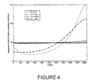
- Figure 4 shows plots of the magnitude of the x-component of the electric field distribution of an example for the case of the standoff structure with an applied voltage of 100 kV and varying conductances.
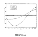
- Figure 4A shows plots of the phase of the x-component of the electric field distribution of an example for the case of the standoff structure with an applied voltage of 100 kV and varying conductances.
- Figure 5 is a view similar to Figure 1 of a modified version of the invention showing the use of a solid rod (as opposed to a hollow column) to form the isolating-section.
- the present invention is based on Applicant's finding that not only may resistive shielding (RS) be used in High Voltage measurements to shield sensors from external sources of interference, but it may be made to be practically as effective at shielding as prior art shielding and to further include improved properties.
- Resistive shielding (RS) relies on resistive materials with conductivities that can be much more readily obtainable than the high permittivities of the materials required for capacitive or dielectric shielding. Resistive materials are abundant and come in many varieties, the potential exists when practicing the present invention to use very thin malleable materials, possibly even a properly designed semi-conductive paint covering the properly.
- the RS system of the present invention relies on selecting resistive materials to form the isolating-section 2 of the invention.
- the materials selected will possess relatively small conductivities, i.e. the isolating-section 2 will possess a resistance per unit of length (measured in the direction between the terminals or electrodes 8 and 10 at the opposite ends of the section 2, in the illustrated arrangement axially of the tube 2) in Ohms( ⁇ )/meter(m) in the range of 25 G ⁇ /m to 50 k ⁇ /m, more preferably 1 G ⁇ /m to 500 k ⁇ /m.
- the conductivity is not uniform and/or the vertical electric field component is not uniform, the relationship among R, A, ⁇ , and L is mathematically more complex but with still the same meaning and that is that the resistance R decreases as the cross-sectional area A increases, increases as the resistivity p increases, and increases as the length L increases.
- the isolating-section 2 will possess a resistance in the range of 25 G ⁇ to 50 k ⁇ .
- the systems of the present invention provide voltage measurements i.e. determine values V d for the voltage V being determined so that errors in V d relative to the actual voltage V due to the influences of external sources are small, preferably less than 6%, preferably less than 1%, more preferably less than 0.3% and most preferably less than 0.1%.
- the basic elements of the invention 1 as schematically shown in Figure 1 include an inner tube or isolating-section 2 having a ''top'' electrode 8 and "bottom" electrode 10 one at each of its axial ends. It will be recognized that the isolating-section 2 need not be positioned with its longitudinal axis vertical. At least one electric field sensor (EFS) 6 (only one is necessary, but more may be used if desired) is mounted at a selected location(s) in the isolating-section 2 (see said Jaeger et al. application referred to above
- the EFS(s) is (are) connected to a detecting unit 12 through optical fiber(s) 11.
- the EFS measurement(s) is(are) used to determine the value V d for the voltage difference V between electrode 8 and electrode 10.
- each EFS When more than one EFS is used, the output of each EFS may be separately measured and subsequently combined with other EFS measurements to determine voltage difference V d , or all EFSs can be put in series, each possibly selected to have a different sensitivity, so that the combination of electric field measurements happens physically by way of light going through the sensors in series to determine said voltage difference, or any combination of separate and series EFSs described above can be used to determine said voltage difference (see said Jaeger at al. application referred to above).
- the invention 1 applied to a standoff 21 for measuring line-to-ground voltage is schematically shown in Figure 2.
- the standoff 21 is formed by the above described basic elements of the invention 1 including the inner tube 2 which is surrounded by an external protective sleeve (tube) 3 having sheds 4 and flanges 13 at axial ends for interfacing with conductive (typically metallic) elements such as stand 5, which happens to also support the standoff 21.
- the external tube 3 and sheds 4 are provided to protect the invention 1 from the outside environment while providing insulation and mechanical support between two ends of the invention.
- the metallic stand 5 is connected to ground schematically indicated at 9 and the top electrode 8 to a HV line.
- a corona ring 7 is suspended near its top electrode 8 where a high voltage is applied so as to moderate the high electric fields that would otherwise be present at the top electrode 8 which may cause flashover.
- the top electrode 8 would be electrically connected to a HV line, and the invention 1 would be used to measure the line-to-ground voltage.
- the isolating-section 2 may, if desired, be made integral with the protecting tube 3 rather than as a separate entity spaced from the tube 3. It is envisioned that a properly selected semi-conductive paint covering a surface of the tube 3 may be used to define the isolating-section 2.
- the invention 1 may be positioned between and connected to any two conductors between which the voltage is to be measured, e.g., the voltage between two phases in a three-phase system.
- d o an inside diameter
- d i a thickness
- L a length
- d i the thickness
- the cross-sectional area A of the isolating-section 2 obviously is a function of d i and d o .
- the area A, the length L, the conductivity ⁇ , the permittivity ⁇ , and the permeability ⁇ of the isolating-section 2 define the admittance shielding AS and, as discussed below with respect to Figure 4 and 4A, are in accordance with the present invention coordinated in a specific manner and so that the conductivity of the material from which the isolating-section 2 is made and the cross-sectional area A of the isolating-section 2 are of selected values to influence the structure of the electric field to conform with that required for effective operation of the invention 1.
- L The choice of L for a given material from which the isolating-section 2 is made depends on many factors. One important factor is safety. The length L should be sufficiently long to ensure safety. The value L will be chosen so that the electric field anywhere in and around the isolating-section 2 is not greater than the break-down strength (field) of the material(s) present under any reasonable operating condition as provided by governing bodies such as the Institute of Electrical and Electronics Engineers (IEEE), the American National Standards Institute (ANSI), the International Electro-technical Commission (IEC), and/or other local and international standards.
- IEEE Institute of Electrical and Electronics Engineers
- ANSI American National Standards Institute
- IEC International Electro-technical Commission
- the minimum length L of the isolating-section is limited by the maximum acceptable electric field intensity (closer electrodes, higher intensities), and the maximum length L of the isolating-section is limited by the desired size and weight of the invention, which is preferably as small as possible.
- cross-sectional area A e.g. thickness d
- the choice of cross-sectional area A is also limited by many factors. Two important practical limitations are size and weight.
- the cross-sectional area A will be chosen so that size and weight will be small enough for installation requirements and mechanical stability.
- the isolating-section 2 need not be tubular or uniform. It can have various different shapes, uniform or non-uniform. For example it can have rectangular cross-section, be hollow or solid, have varying materials (having different resistivities) in various locations in the isolating-section. The choice of the shape and the material depends very much on the application and the principles as taught in this patent application can be used to determine suitable designs for an isolating-section to be used in a particular application.
- this power P is taken from the conductors being measured for voltage difference.
- this amount must be kept sufficiently small for the invention to be acceptable, so the maximum conductivity must also be sufficiently small.
- Admittance of, say, a solid rod of material is directly related to the conductivity and permittivity of the material and the cross-sectional area of the rod (related to "d o " and “d i ”) and inversely related to the length of the rod (related to "L"). It is therefore possible to obtain a particular admittance by varying the geometry of the rod, which is what is equivalently done in certain prior art for which the equivalent rod is made of air and the electrode geometries at the ends of the rod are varied, e.g. they are brought very close together and the rod is made very short until the admittance between electrodes is high enough to provide sufficient shielding.
- the permittivity can be increased. In fact, both permittivity and conductivity can be increased together to improve shielding.
- the present invention an increase in the conductance is used, which permits a trade-off between varying geometry and varying material conductivity.
- the electrodes need not be brought close together (requiring the use of special insulation) nor does the cross-sectional area of isolating-section 2 have to be increased (resulting in larger size and weight), but instead the present invention takes advantage of the flexibility in changing the material properties of the isolating-section 2, specifically, its conductivity.
- the material from which 2 is constructed causes a structured electric field distribution in and around 2.
- An example of a potentially useful resistive material forming the isolating-section is polyethylene doped with carbon black.
- Different conductivities can be attained by varying the doping levels of carbon black.
- a thin film (approximately 0.1 mm thick) can be made of polyethylene containing carbon black uniformly distributed therethrough at levels ranging between 40 phr to 50 phr (parts per hundred) and could be positioned along the inside of the protective sleeve (protective tube) 3 for good resistive shielding in a 230 kV class electric field sensor voltage transducer (EFSVT).
- EFSVT electric field sensor voltage transducer
- the overall accuracy of the system improves if the magnitude of admittance is greater, i.e., the field distribution is less affected by external influences.
- Typical external influences include the presence of other conductors at various potentials and the effects of pollution on and around said external tube 3 and its sheds 4 and other nearby structures, conducting or non-conducting, mobile or stationary.
- the effects of many of these influences are not that severe since other structures are usually located at distances that are large enough for safety reasons and are determined using various relevant IEEE, ANSI, IEC, and/or other standards or guidelines for each voltage class.
- the present invention is a significant advancement over prior art in that the overall accuracy of the system is achieved, i.e., sufficient admittance shielding is accomplished, by increasing the conductivity ⁇ of the material forming the isolating-section 2 which increases the conductance G of the isolating-section 2.
- L can be selected to be large enough to prevent high electric field intensities due to conductors in close proximity and, therefore, eliminate the need for special insulation resulting in a simpler, safer voltage transducer.
- the conductance G of the isolating-section 2 can be 10 nS (1x10 -8 S) for an isolating-section 2 which is 2.07 meters long (measured parallel to the longitudinal axis of the isolating-section 2).
- EFSs electric field sensors
- EFSs small optical EFSs such as Integrated Optics Electric Field Sensors (IOEFSs) more specifically Integrated Optics Pockels Cell (IOPC) EFSs as described in the above referred to Jaeger patent and small bulk-optics Pockels cells.
- IEFSs Integrated Optics Electric Field Sensors
- IOPC Integrated Optics Pockels Cell
- Other suitable EFSs may be used.
- Mach-Zehnder type field sensors such as those with domain inversion in one branch may be used (see for example N.A.F. Jaeger and L. Huang "Push-Pull Integrated-optics Mach-Zehnder Interferometer with Domain Inversion in One Branch” Optics Letters, vol. 20, no. 3, pp. 288-290, February 1995, or a sensor as described in US patent 5,267,336 issued November 30, 1993 to Sriram et al.).
- EFS examples can be found in US Patents: 4,929,830 ''Fiber-optic electric field sensor with piezoelectric body sensor," issued May 29, 1990 to K. Bohnert, M. Kaufmann, and J. Nehring; 5,053,694 ''Device for measuring an electric field” issued Oct. 1,1991, to K Bohnert and J. Nehring; 5,053,693 "Fibreoptical sensor” issued Oct. 1,1991, to K Bohnert and W. Buser; 5,475,773 ''Fiber-optic quartz voltage sensor” issued Dec. 12, 1995, to M. Ingold; and 5,731,579 "Electro-optical voltage sensor head” issued March 24, 1998, to G.K. Woods.
- VT that has to meet the class 3P relaying standard according to IEC standard 60044-2 (1997-02); basically, the VT is allowed to have ⁇ 3% error in V d in measuring the voltage magnitude and ⁇ 2° phase angle error in measuring the phase of the power frequency voltage, typically a 60Hz or 50Hz signal, (of course there are many other requirements in the standard that are out of the scope of this brief example); so, in this case, the statement "do not change ...
- shielding will be applied so that the isolating-section 2 will reduce the error in V d to be preferably less than 25% of the error in V d that would be obtained if no shielding were provided.
- the shielding will be provided to reduce the error preferably to less than 6%, more preferably to less than 1%, and more preferably to less than 0.3% as above described.
- the output of an EFS is a measure of the intensity of a particular component of the electric field inside the EFS; see for example N.A.F. Jaeger and F. Rahmatian, "Integrated Optics Pockels Cell High-Voltage Sensor," IEEE Trans. on Power Delivery, vol. 10, no. 1, pp. 127-134, Jan. 1995. It is desired to use this sensory ability to measure the voltage between the top 8 and bottom 10 electrodes of the present invention; for example, line-to-ground voltage on a power line connected to the top electrode 8 when the stand 5 and bottom electrode 10 are grounded.
- a suitable EFS could be used by being appropriately placed somewhere in a standoff structure 21 attached to the transmission line.
- the standoff 21 is formed by the basic elements of the invention 1 including the inner tube 2 which is surrounded by an external protecting tube 3 having sheds 4 and flanges 13 at axial ends for interfacing with conductive (typically metallic) elements such as stand 5, which happens to also support the invention 1 in this case.
- the EFS(s) output(s) is(are) used to deduce the voltage on the transmission line. Since the EFS output depends on the electric field the standoff structure 21 must be modified in such a way so as to reduce the coupling effects of other HV transmission lines and any other structures in the vicinity.
- systems may be designed to measure any reasonable voltage.
- the economic (and safety) benefits i.e. practical range of usage, will be at higher voltages in the several-thousand-volt ranges.
- the quasistatic electromagnetic field that exists in any space containing at least one electrical source can be approximately represented by a network of nodes locally interconnected through passive circuit elements, including capacitances, inductances, and conductances, and at least one equivalent current or voltage source (See D. M. Pozar, Microwave Engineering, Addison-Wesley, 1990 for details).
- Each node represents a point in space and is connected to other nodes that represent neighboring points in space.
- the voltage on each node represents the electric potential at the respective point in space.
- the standoff 21 can be approximately modeled as a lumped linear admittance network of N stacked units. Each unit has a central self-admittance Y c , a center-to-isolating-section admittance Y ci , an isolating-section self-admittance Y i , an intemal-to-external coupling admittance Y ie , an external self-admittance Y p , a ground admittance Y g , a line admittance Y 1 , and an external line and source admittance Y s .
- An EFS e.g. IOPC is physically located inside the isolating-section 2 and in effect locally measures the gradient of the electric potential distribution that exists along the center of the isolating-section 2 and that is represented by the voltages of the internal unit nodes connecting the central self-admittances Y c .
- the self-admittance Y of the isolating-section 2 is known to be a function of the N self-admittances Y i .
- the standoff 21 is viewed as a composition of individual vertically stacked units.
- Y c represents the self-admittance of a region of space along the center of a unit, and since this region is typically occupied by air, Y c is primarily capacitive.
- Y i represents the self-admittance of the section of material of the isolating-section 2 in a unit
- Y p represents the self-admittance of the section of external tube 3 material, shed 4 material, and possibly existing contaminant material in a unit.
- each of the associated admittances (Y c , Y i , Y p ) is a conductance, a capacitance, an inductance, or a combination of these.
- Y ci represents the coupling between the region of space along the center of a unit and the isolating-section 2 in that unit.
- Y ie represents the coupling between the isolating-section 2 in a unit and the external tube 3, sheds 4, and possibly existing contaminants in that unit.
- Y g , Y 1 , and Y s represent the coupling between the external tube 3, sheds 4 and possibly existing contaminants in a unit and ground, the high-voltage line being measured, and other lines or sources having an effective value of V', respectively.
- Y ci , Y ie , Y g , Y 1 , and Y s are primarily capacitances (air coupling). Also, except for very high frequencies, the inductances mentioned above are negligibly small.
- a fixed one-to-one relationship between the voltage distribution at the EFS location and the line voltage must be achieved. This can be done by ensuring that the magnitudes of isolating-section self-admittances Y i are much greater than those of any other admittances that may be variable, e.g., external admittances Y p , Y g , and Y 1 . In this case the current from line to ground is primarily confined to the internal branches of the units with any changes in the other admittances having negligible impact on the internal current distribution.
- Y can be increased in magnitude to improve isolation and reduce external coupling effects in the region.
- Five parameters of the isolating-section 2 can be varied to increase the magnitude of admittance Y:
- any isolating-section 2 consisting of a material of fixed electrical properties a shorter length L and/or greater cross-sectional area A of the isolating-section 2 (see Figures 1 and 2) gives a smaller impedance and therefore a larger Y.
- a higher conductivity ⁇ , higher permittivity ⁇ , and/or lower permeability ⁇ , of the isolating-section 2 gives a larger Y.
- varying ⁇ as taught by the present invention allows great flexibility in achieving a desired Y.
- the choice of values of parameters (1) through (5) depends on considerations such as the accuracy and safety requirements for the voltage sensor.
- the high admittance material of the isolating-section 2 should be more centrally confined improving isolation of the field in the center from stray field effects.
- the proper design procedure involves modeling the voltage sensor column, considering the restrictions provided under various relevant standards (such as those mentioned above), considering the accuracy requirements, and considering the availability of proper materials, their electrical properties, weight, heat generation and dissipation, and cost to provide an economical, accurate (for the intended application), and safe voltage sensor.
- EFSVT examples having different inner tube resistances of infinity, 10 12 , 10 9 , 10 8 , 5 ⁇ 10 7 , and 10 6 ⁇ .
- the relative permittivities of the inner and outer tubes are 5 and the relative permittivity of the surrounding medium is 1 (air). These resistances correspond to conductances of zero, 1 pS, 1 nS, 10 nS, 20 nS, and 1 ⁇ S, respectively.
- a single EFS that measures the component E x of the electric field that is parallel to the axis of the isolating-section at a point in space is assumed to be located halfway between the top and bottom electrodes on the center axis.
- the electric field E around the standoff is computed using the finite element method.
- Test simulations are set up to measure the performance of the EFSVT designs in different environments.
- the VT is used to measure the voltage between the top and bottom electrodes with the bottom electrode taken as the reference.
- the applied voltage is sinusoidal with a frequency of 60 Hertz.
- the voltage phase is arbitrarily chosen as the reference for the phase information given in these examples (see Tables).
- a layer of water resting on the sheds and having a uniform thickness of 0.25 mm is simulated for each EFSVT with varying degrees of water contamination represented by resistivities of 10 8 ⁇ -cm, 10 5 ⁇ -cm, and 100 ⁇ -cm.
- resistivities 10 8 ⁇ -cm, 10 5 ⁇ -cm, and 100 ⁇ -cm.
- This case is simulated for isolating-section resistances of ⁇ , 10 12 , 10 9 , 10 8 , 5 ⁇ 10 7 , and 10 6 ⁇ .
- the measured or determined voltage V d can be represented by an amplitude and a phase. Though in general the output of the VT gives an instantaneous reading of voltage continuously in time.
- E is sinusoidal with a frequency of 60 Hz and can also be represented by a magnitude and phase.
- the voltage measured V d can be determined from the EFS outputs with where E x,i is the output of the ith EFS, C i is the calibration constant and/or gain factor of the ith EFS, and n is the total number of EFSs, as is described in the above referred to Jaeger et al. application.
- the error between the actual voltage V applied and the voltage measured V d will be expressed in terms of an amplitude error and a phase error.
- the magnitude of C is a constant of proportionality and is determined based on the applied voltage that is to be measured; in the case examples, we are looking for normalized or percentage errors and we are not concerned with the actual voltage class. Also, the percentage errors given are relative to (percentage of) the amplitude of the applied voltage signal.
- Table 1 shows results for the Case 1 simulations. It can be observed from these results that generally as the isolating-section resistance decreases, the amplitude error incurred by the presence of the uniform layer of water resting on the sheds decreases significantly. The phase error also decreases as the isolating-section resistance decreases for isolating-section resistances below 1 G ⁇ i.e. for isolating-section conductances greater than 1 nS.
- Table 2 and Table 3 show results for Case 2 and Case 3, respectively. Also, test simulations here focus on inner tube resistances of 50 M ⁇ and 100 M ⁇ since they are in the range of the lowest allowable resistance values for practical high-voltage applications for 230 kV class voltage transducers. The effect of dryband conditions are studied here since these are expected to be practically some of the worst-case scenarios in terms of the effects of external causes that disturb the electric field inside the isolating-section. Again, greatly reduced errors in phase and amplitude due to a decreased isolating-section resistance is evident in the tables.
- Inner tube resistance (M ⁇ ) Water resistivity (M ⁇ -cm) Amplitude error in % Phase error in minutes ⁇ 100 -0.65 0.99 1000000 100 -0.60 0.85 1000 100 1.30 -4.62 100 100 0.04 6.85 50 100 0.01 3.50 1 100 0.00 0.07 ⁇ 0.1 -11.51 677.91 1000000 0.1 -11.17 664.51 1000 0.1 -7.99 -45.09 100 0.1 -0.55 9.57 50 0.1 -0.30 5.70 1 0.1 -0.01 0.13 ⁇ 0.0001 -82.10 4.57 1000000 0.0001 -80.64 2.69 1000 0.0001 -31.06 -1057.18 100 0.0001 -0.62 -190.01 50 0.0001 -0.17 -96.19 1 0.0001 0.00 -1.93 EFSVT Simulation Results for Uniform Water Deposit and Upper Dryband.
- Inner tube resistance (M ⁇ ) Water resistivity (M ⁇ -cm) Amplitude error in % Phase error in minutes ⁇ 100 0.07 0.14 100 100 0.04 8.02 50 100 0.01 4.06 ⁇ 0.1 -6.10 113.34 100 0.1 0.53 14.61 50 0.1 0.23 7.80 ⁇ 0.0001 97.58 -5320.43 100 0.0001 5.95 1282.49 50 0.0001 2.23 649.49 EFSVT Simulation Results for Uniform Water Deposit and Lower Dryband.
- Inner tube resistance (M ⁇ ) Water resistivity (M ⁇ -cm) Amplitude error in % Phase error in minutes ⁇ 100 -0.23 0.53 100 100 0.06 8.95 50 100 0.02 4.62 ⁇ 0.1 -9.18 383.81 100 0.1 -0.21 18.74 50 0.1 -0.14 10.59 ⁇ 0.0001 86.08 -557.53 100 0.0001 -7.73 -395.75 50 0.0001 -2.80 -251.99
- the simplified model given in Figure 3 can be used to show that when Y i is relatively large, e.g., when significant resistive shielding is present, the effect of external influences on the electric field distribution inside the resistive shield, i.e., column center, is smaller as compared to when Y i is relatively small.
Landscapes
- Physics & Mathematics (AREA)
- General Physics & Mathematics (AREA)
- Measuring Instrument Details And Bridges, And Automatic Balancing Devices (AREA)
- Measuring Fluid Pressure (AREA)
- Air Bags (AREA)
- Measurement Of Current Or Voltage (AREA)
Claims (23)
- Vorrichtung (1) zum Messen von Spannung in einer Hochspannungsumgebung mit:wobei der isolierende Bereich (2) eine ausgewählte elektrische Widerstandscharakteristik aufweist, so dass er eine ausreichende Abschirmung für den mindestens einen Ort darstellt, um so jeglichen Fehler bei Vd zu reduzieren, der anderenfalls in der Abwesenheit des isolierenden Bereichs aufgrund jeglicher externer elektrischer. Feldstörquellen auftreten würde.einem elektrisch isolierenden Bereich (2);einem Paar von voneinander beabstandeten Leitern, die an einen ersten bzw. zweiten Anschluss (8, 10) angeschlossen sind, zwischen welchen eine Spannungsdifferenz V zu bestimmen ist, wobei sich ein erster der Leiter an dem ersten Ende des isolierenden Bereichs und ein zweiter der Leiter (10) entfernt von dem ersten Ende an dem zweiten Ende des isolierenden Bereichs befindet, wobei die Enden vorgesehen sind, elektrisch mit dem ersten bzw. zweiten Anschluss verbunden zu werden;mindestens einem elektrischen Feldsensor (6), der elektrisches Feld an mindestens einem Ort innerhalb oder in der Nähe des isolierenden Bereichs erfasst; undeinem Detektor (12) zum Bestimmten eines Werts Vd für die Spannungsdifferenz V basierend auf dem elektrischen Feld, das von dem mindestens einen elektrischen Feldsensor erfasst wird;
- Vorrichtung nach Anspruch 1, bei der die ausgewählte Widerstandscharakteristik des isolierenden Bereichs (2) derart ist, dass sie einen Widerstand pro Längeneinheit in dem Bereich zwischen 25 GΩ/m und 50 kΩ/m zwischen dem Paar von einander beabstandeten Leitern aufweist.
- Vorrichtung nach Anspruch 1, bei der die ausgewählte Widerstandscharakteristik des isolierenden Bereichs (2) derart ist, dass sie einen Widerstand in dem Bereich zwischen 25 GΩ und 50 kΩ zwischen dem Paar von voneinander beabstandeten Leitern aufweist.
- Vorrichtung nach Anspruch 2, bei der die ausgewählte Widerstandscharakteristik des isolierenden Bereichs (2) derart ist, dass sie einen Widerstand pro Längeneinheit in dem Bereich zwischen 1 GΩ/m und 500 kΩ/m zwischen dem Paar von voneinander beabstandeten Leitern aufweist.
- Vorrichtung nach einem der vorangehenden Ansprüche, wobei die ausgewählte Widerstandscharakteristik des isolierenden Bereichs (2) derart ist, dass sie jeglichen Fehler bei Vd auf weniger als 25 % des Fehlers reduziert, der anderenfalls in der Abwesenheit des isolierenden Bereichs auftreten würde.
- Vorrichtung nach Anspruch 5, wobei die ausgewählte Widerstandscharakteristik des isolierenden Materials (2) derart ist, dass sie jeglichen Fehler bei Vd auf weniger als 6 % des Fehlers reduziert, der anderenfalls in der Abwesenheit des isolierenden Bereichs auftreten würde.
- Vorrichtung nach Anspruch 6, wobei die ausgewählte Widerstandscharakteristik des isolierenden Bereichs (2) derart ist, dass sie jeglichen Fehler bei Vd auf weniger als 1% des Fehlers reduziert, der anderenfalls in der Abwesenheit des isolierenden Bereichs auftreten würde.
- Vorrichtung nach Anspruch 7, wobei die ausgewählte Widerstandscharakteristik des isolierenden Bereichs (2) derart ist, dass sie jeglichen Fehler bei Vd auf weniger als 0,3 % des Fehlers reduziert, der anderenfalls in der Abwesenheit des isolierenden Bereichs auftreten würde.
- Vorrichtung nach einem der vorangehenden Ansprüche, bei der der isolierende Bereich (2) hohl ist.
- Vorrichtung nach einem der vorangehenden Ansprüche, bei der der isolierende Bereich (2) aus einem mit Kohlenstoffschwarz dotierten Polyethylen besteht.
- Vorrichtung nach einem der vorangehenden Ansprüche, die weiterhin eine Schutzhülse (3) zum Schützen des isolierenden Bereichs (2) gegenüber der Umgebung aufweist.
- Vorrichtung nach einem der vorangehenden Ansprüche, wobei der elektrische Feldsensor (6) ein optischer elektrischer Feldsensor ist.
- Vorrichtung nach Anspruch 9, wobei der isolierende Bereich (2) ein hohler Rohrwiderstand ist und wobei der mindestens eine elektrische Feldsensor (6) innerhalb des hohlen Rohrwiderstands angeordnet ist.
- Vorrichtung nach Anspruch 1, die weiterhin eine hohle Isolatorsäure zum Abstützen des ersten und zweiten Anschlusses (8, 10) aufweist, wobei der isolierende Bereich (2) und der mindestens eine elektrische Feldsensor (6) innerhalb der hohlen Isolatorsäule angeordnet sind.
- Vorrichtung nach Anspruch 14, bei der der isolierende Bereich (2) eine Widerstandsbeschichtung auf einer Oberfläche der hohlen Isolatorsäure aufweist.
- Vorrichtung nach einem der vorangehenden Ansprüche, die weiterhin eine Mehrzahl der elektrischen Feldsensoren (6) umfasst, die in dem isolierenden Bereich (2) zwischen den ersten und dem zweiten voneinander beabstandeten Leitern angeordnet sind, wobei der Detektor (12) den Wert Vd, der die Spannung V zwischen den ersten und dem zweiten voneinander beabstandeten Leitern anzeigt, als Funktion des elektrischen Feldausgangssignals bestimmt, das mit jedem der Mehrzahl von elektrischen Feldsensoren verbunden ist.
- Vorrichtung nach Anspruch 12, wobei jeder der optischen elektrischen Feldsensoren (6) über eine optische Faser (11) an den Detektor (12) angeschlossen ist.
- Vorrichtung nach Anspruch 12, die weiterhin eine Mehrzahl der optischen elektrischen Feldsensoren umfasst, die so an den Detektor (12) angeschlossen sind, dass die Ausgabe jedes optischen Sensors separat bestimmt und anschließend mit anderen Sensormessungen kombiniert werden kann, um den Spannungsdifferenzwert Vd zu bestimmen.
- Vorrichtung nach Anspruch 12, die weiterhin eine Mehrzahl der optischen elektrischen Feldsensoren umfasst, die so in Reihe an den Detektor (12) angeschlossen sind, dass eine Kombination der elektrischen Feldmessungen physikalisch erfolgt, indem Licht in Reihe durch jeden Sensor hindurch tritt, um den Spannungsdifferenzwert Vd zu bestimmen.
- Vorrichtung nach Anspruch 19, wobei jeder der Mehrzahl von optischen elektrischen Feldsensoren in seiner Empfindlichkeit variiert.
- Verfahren zum Messen einer Spannungsdifferenz V zwischen ersten und zweiten voneinander beabstandeten Leitern, die an einen ersten bzw. einen zweiten Anschluss (8, 10) angeschlossen sind, in einer Hochspannungsumgebung, mit den Schritten:wobei der isolierende Bereich (2) so vorgesehen ist, dass er eine ausgewählte elektrische Widerstandscharakteristik aufweist, so dass er ausreichende Abschirmung für den mindestens einen Ort bereitstellt, so dass jeglicher Fehler bei Vd reduziert wird, der anderenfalls in der Abwesenheit des isolierenden Bereichs aufgrund jeglicher externer elektrischen Feldquellen auftreten würde.Bereitstellen eines elektrisch isolierenden Bereichs zwischen den ersten und zweiten voneinander beabstandeten Leitern;räumliches Anordnen mindestens einen elektrischen Feldsensors (6), der elektrisches Feld erfasst, an mindestens einem Ort zwischen dem ersten und dem zweiten Leiter und innerhalb oder in der Nähe des isolierenden Bereichs; undBestimmen eines Werts Vd für die Spannungsdifferenz V basierend auf dem elektrischen Feld, das von dem mindestens einen elektrischen Feldsensor erfasst wird, unter Verwendung eines Detektors (1);
- Verfahren nach Anspruch 21, bei dem der Wert von Vd unter Verwendung eines optischen Sensors bestimmt wird.
- Verfahren nach Anspruch 21, bei dem der isolierende Bereich als ein hohler Rohrwiderstand bereitgestellt wird und der elektrische Feldsensor innerhalb des isolierenden Bereichs angeordnet wird.
Applications Claiming Priority (3)
| Application Number | Priority Date | Filing Date | Title |
|---|---|---|---|
| US09/503,897 US6380725B1 (en) | 2000-02-15 | 2000-02-15 | Voltage sensor |
| US503897 | 2000-02-15 | ||
| PCT/CA2001/000103 WO2001061365A1 (en) | 2000-02-15 | 2001-01-30 | Voltage sensor |
Publications (2)
| Publication Number | Publication Date |
|---|---|
| EP1256004A1 EP1256004A1 (de) | 2002-11-13 |
| EP1256004B1 true EP1256004B1 (de) | 2004-11-03 |
Family
ID=24003980
Family Applications (1)
| Application Number | Title | Priority Date | Filing Date |
|---|---|---|---|
| EP01902210A Expired - Lifetime EP1256004B1 (de) | 2000-02-15 | 2001-01-30 | Spannungssensor |
Country Status (10)
| Country | Link |
|---|---|
| US (1) | US6380725B1 (de) |
| EP (1) | EP1256004B1 (de) |
| JP (1) | JP2003523519A (de) |
| CN (1) | CN1193235C (de) |
| AT (1) | ATE281651T1 (de) |
| AU (1) | AU2001229926A1 (de) |
| BR (1) | BR0108366B1 (de) |
| CA (1) | CA2398082C (de) |
| DE (1) | DE60106872T2 (de) |
| WO (1) | WO2001061365A1 (de) |
Families Citing this family (21)
| Publication number | Priority date | Publication date | Assignee | Title |
|---|---|---|---|---|
| JP2003130893A (ja) * | 2001-10-25 | 2003-05-08 | Hitachi Ltd | シールドを有する電気回路 |
| DE10206073B8 (de) * | 2002-02-13 | 2006-09-14 | Tutech Innovation Gmbh | Vorrichtung zur Erfassung leitungsgeführter elektromagnetischer Pulse |
| EP1660896A4 (de) * | 2003-09-05 | 2012-02-29 | James N Blake | Zeitlich gemultiplextes optisches messsystem |
| US7123032B2 (en) * | 2003-12-04 | 2006-10-17 | Fieldmetrics, Inc. | Voltage sensor and dielectric material |
| US7129693B2 (en) * | 2004-07-19 | 2006-10-31 | Fieldmetrics, Inc. | Modular voltage sensor |
| US7528612B2 (en) * | 2006-09-29 | 2009-05-05 | Rockwell Automation Technologies, Inc. | System and method for monitoring a motor control center |
| US7561412B2 (en) * | 2006-09-29 | 2009-07-14 | Rockwell Automation Technologies, Inc. | System and method for automatically securing a motor control center |
| WO2008065196A2 (en) * | 2006-11-30 | 2008-06-05 | North Sensor A/S | Faraday effect current sensor |
| FR2958755B1 (fr) * | 2010-04-13 | 2012-09-21 | Schneider Electric Ind Sas | Dispositif de mesure a diviseur de tension electrique. |
| WO2011154029A1 (en) | 2010-06-07 | 2011-12-15 | Abb Research Ltd | High-voltage sensor with axially overlapping electrodes |
| CN101951002A (zh) * | 2010-09-29 | 2011-01-19 | 福州大学 | 高电压系统电场感应式信号检测电路电源 |
| EP2479581A1 (de) | 2011-01-21 | 2012-07-25 | PowerSense A/S | Wechsel- oder Gleichstromübertragungssystem und Verfahren zum Messen einer Spannung |
| US9093867B2 (en) | 2011-09-23 | 2015-07-28 | Eaton Corporation | Power system including an electret for a power bus |
| US8791831B2 (en) | 2011-09-23 | 2014-07-29 | Eaton Corporation | System including an indicator responsive to an electret for a power bus |
| EP2693223B8 (de) * | 2012-08-03 | 2021-09-08 | ABB Schweiz AG | Spannungsmessvorrichtung mit einem Isolierkörper |
| TWI531800B (zh) | 2014-09-16 | 2016-05-01 | 財團法人工業技術研究院 | 非接觸式雙線電源線電壓感測器及其安裝位置變動補償方法 |
| CN104237934A (zh) * | 2014-09-29 | 2014-12-24 | 中国地质大学 | 差动式压电地震数字检波器 |
| CN105629049A (zh) * | 2016-03-30 | 2016-06-01 | 三峡大学 | 一种基于高斯求积算法的光学电压互感器 |
| PL233936B1 (pl) * | 2017-12-27 | 2019-12-31 | Siec Badawcza Lukasiewicz – Instytut Tele I Radiotechniczny | Układ do eliminacji zakłóceń w kablach pomiarowych |
| CN108828493B (zh) * | 2018-06-21 | 2021-02-09 | 清华大学 | 消除温度和其它相电场对光学电压互感器精度影响的方法 |
| RU185716U1 (ru) * | 2018-06-28 | 2018-12-14 | Владимир Ильич Крючков | Шинный датчик высокого напряжения |
Family Cites Families (19)
| Publication number | Priority date | Publication date | Assignee | Title |
|---|---|---|---|---|
| DE2341074B2 (de) | 1973-08-10 | 1976-10-21 | Siemens AG, 1000 Berlin und 8000 München | Messeinrichtung fuer die spannung zwischen einem innenleiter und dem aussenrohr einer gekapselten hochspannungsschaltanlage |
| DE3886699D1 (de) | 1987-11-05 | 1994-02-10 | Asea Brown Boveri | Faseroptischer Sensor. |
| EP0316635B1 (de) | 1987-11-13 | 1994-09-21 | ABB Management AG | Faseroptischer Spannungssensor |
| JP2737056B2 (ja) | 1988-12-01 | 1998-04-08 | 株式会社共和電業 | 可動高電圧体の物理量測定システムにおけるシールド方法 |
| EP0393382B1 (de) | 1989-04-07 | 1994-06-01 | Asea Brown Boveri Ag | Vorrichtung zum Messen eines eletrischen Feldes |
| DE59004780D1 (de) | 1989-12-22 | 1994-04-07 | Asea Brown Boveri | Faseroptischer Sensor. |
| US5029273A (en) | 1990-02-02 | 1991-07-02 | The University Of British Columbia | Integrated optics Pockels cell voltage sensor |
| CH682190A5 (de) | 1991-04-22 | 1993-07-30 | Asea Brown Boveri | |
| JPH05273256A (ja) | 1992-03-24 | 1993-10-22 | Furukawa Electric Co Ltd:The | 碍子内蔵型光電圧センサ |
| US5267336A (en) | 1992-05-04 | 1993-11-30 | Srico, Inc. | Electro-optical sensor for detecting electric fields |
| DE4229449A1 (de) | 1992-09-03 | 1994-03-10 | Abb Research Ltd | Faseroptischer Quarz-Spannungs-Sensor |
| TW224513B (de) | 1992-11-20 | 1994-06-01 | Matsushita Electric Ind Co Ltd | |
| GB9308426D0 (en) | 1993-04-23 | 1993-06-09 | Roster Control Syst Ltd | Watchmans clock system |
| WO1994025973A1 (en) * | 1993-04-29 | 1994-11-10 | Lindsey Manufacturing Company | Integrated electrical system |
| US5731579A (en) | 1995-12-11 | 1998-03-24 | Lockheed Idaho Technologies Company | Electro-optical voltage sensor head |
| US5892357A (en) | 1995-12-08 | 1999-04-06 | Lockheed Martin Idaho Technologies Company | Electro-optic voltage sensor for sensing voltage in an E-field |
| DE59712933D1 (de) | 1996-08-23 | 2008-05-15 | Abb Schweiz Ag | Messvorrichtung für eine metallgekapselte, gasisolierte Hochspannungsanlage |
| FR2764390B1 (fr) * | 1997-06-06 | 1999-07-16 | Gec Alsthom T D Balteau | Capteur electro-optique a diviseur de tension massif |
| US6252388B1 (en) | 1998-12-04 | 2001-06-26 | Nxtphase Corporation | Method and apparatus for measuring voltage using electric field sensors |
-
2000
- 2000-02-15 US US09/503,897 patent/US6380725B1/en not_active Expired - Lifetime
-
2001
- 2001-01-30 CA CA002398082A patent/CA2398082C/en not_active Expired - Lifetime
- 2001-01-30 WO PCT/CA2001/000103 patent/WO2001061365A1/en active IP Right Grant
- 2001-01-30 JP JP2001560700A patent/JP2003523519A/ja active Pending
- 2001-01-30 EP EP01902210A patent/EP1256004B1/de not_active Expired - Lifetime
- 2001-01-30 DE DE60106872T patent/DE60106872T2/de not_active Expired - Lifetime
- 2001-01-30 AU AU2001229926A patent/AU2001229926A1/en not_active Abandoned
- 2001-01-30 BR BRPI0108366-0B1A patent/BR0108366B1/pt not_active IP Right Cessation
- 2001-01-30 AT AT01902210T patent/ATE281651T1/de not_active IP Right Cessation
- 2001-01-30 CN CN01805024.7A patent/CN1193235C/zh not_active Expired - Fee Related
Also Published As
| Publication number | Publication date |
|---|---|
| EP1256004A1 (de) | 2002-11-13 |
| CA2398082A1 (en) | 2001-08-23 |
| CN1193235C (zh) | 2005-03-16 |
| US6380725B1 (en) | 2002-04-30 |
| BR0108366A (pt) | 2003-03-11 |
| AU2001229926A1 (en) | 2001-08-27 |
| DE60106872D1 (de) | 2004-12-09 |
| ATE281651T1 (de) | 2004-11-15 |
| CA2398082C (en) | 2010-01-05 |
| DE60106872T2 (de) | 2005-12-29 |
| WO2001061365A1 (en) | 2001-08-23 |
| BR0108366B1 (pt) | 2013-11-26 |
| CN1418312A (zh) | 2003-05-14 |
| JP2003523519A (ja) | 2003-08-05 |
Similar Documents
| Publication | Publication Date | Title |
|---|---|---|
| EP1256004B1 (de) | Spannungssensor | |
| EP1137950B1 (de) | Spannungssensor | |
| JP6050309B2 (ja) | 高電圧測定システム | |
| US7129693B2 (en) | Modular voltage sensor | |
| Rahmatian et al. | 230 kV optical voltage transducers using multiple electric field sensors | |
| US7126348B2 (en) | Method and a device for voltage measurement in a high-voltage conductor | |
| Bobowski et al. | Calibrated single-contact voltage sensor for high-voltage monitoring applications | |
| EP2508898A1 (de) | Schutzverfahren für Hochspannungsmessungen | |
| Metwally | D-dot probe for fast-front high-voltage measurement | |
| US20050122122A1 (en) | Voltage sensor and dielectric material | |
| He et al. | Potential distribution analysis of suspended-type metal-oxide surge arresters | |
| Takuma et al. | Numerical calculation of electric fields with a floating conductor | |
| Chavez et al. | Accurate voltage measurement with electric field sampling using permittivity-shielding | |
| CN111273070B (zh) | 一种串联式交流高压母线测量装置及方法 | |
| RU111680U1 (ru) | Устройство для измерения напряжения на высоковольтных линиях электропередач | |
| Chavez et al. | 230 kV optical voltage transducer using a distributed optical electric field sensor system | |
| CN107144717A (zh) | 纳米材料介电屏蔽型电子式光学电压互感器 | |
| Rao et al. | Development and experimental evaluation of leakage current measurement sensor for electrical power apparatus | |
| Rahmatian et al. | Wide-band 138 kV distributed-sensor optical voltage transducer: study of accuracy under pollution and other field disturbances | |
| Rao et al. | Condition Monitoring of GIS Surge Arresters | |
| Van der Merwe | Modelling and performance evaluation of a three-phase capacitive voltage sensor topology | |
| Chavez et al. | Integrated-optic voltage transducer for high-voltage applications | |
| Edwards et al. | Portable ADSS surface contamination meter | |
| Ahmed et al. | Measurement and prediction of microshock currents and voltages in an HV laboratory | |
| Kuzenbayev | Dual Capacitive Probe Method for Non-contact High Voltage Measurements |
Legal Events
| Date | Code | Title | Description |
|---|---|---|---|
| PUAI | Public reference made under article 153(3) epc to a published international application that has entered the european phase |
Free format text: ORIGINAL CODE: 0009012 |
|
| 17P | Request for examination filed |
Effective date: 20020726 |
|
| AK | Designated contracting states |
Kind code of ref document: A1 Designated state(s): AT BE CH CY DE DK ES FI FR GB GR IE IT LI LU MC NL PT SE TR |
|
| AX | Request for extension of the european patent |
Free format text: AL;LT;LV;MK;RO;SI |
|
| RIN1 | Information on inventor provided before grant (corrected) |
Inventor name: CHAVEZ, PATRICK, PABLO Inventor name: RAHMATIAN, FARNOOSH Inventor name: JAEGER, NICOLAS, AUGUST, FLEMING Inventor name: YAKYMYSHYN, CRISTOPHER, PAUL |
|
| 17Q | First examination report despatched |
Effective date: 20030212 |
|
| GRAP | Despatch of communication of intention to grant a patent |
Free format text: ORIGINAL CODE: EPIDOSNIGR1 |
|
| GRAS | Grant fee paid |
Free format text: ORIGINAL CODE: EPIDOSNIGR3 |
|
| GRAA | (expected) grant |
Free format text: ORIGINAL CODE: 0009210 |
|
| AK | Designated contracting states |
Kind code of ref document: B1 Designated state(s): AT BE CH CY DE DK ES FI FR GB GR IE IT LI LU MC NL PT SE TR |
|
| PG25 | Lapsed in a contracting state [announced via postgrant information from national office to epo] |
Ref country code: AT Free format text: LAPSE BECAUSE OF FAILURE TO SUBMIT A TRANSLATION OF THE DESCRIPTION OR TO PAY THE FEE WITHIN THE PRESCRIBED TIME-LIMIT Effective date: 20041103 Ref country code: FI Free format text: LAPSE BECAUSE OF FAILURE TO SUBMIT A TRANSLATION OF THE DESCRIPTION OR TO PAY THE FEE WITHIN THE PRESCRIBED TIME-LIMIT Effective date: 20041103 Ref country code: TR Free format text: LAPSE BECAUSE OF FAILURE TO SUBMIT A TRANSLATION OF THE DESCRIPTION OR TO PAY THE FEE WITHIN THE PRESCRIBED TIME-LIMIT Effective date: 20041103 Ref country code: BE Free format text: LAPSE BECAUSE OF FAILURE TO SUBMIT A TRANSLATION OF THE DESCRIPTION OR TO PAY THE FEE WITHIN THE PRESCRIBED TIME-LIMIT Effective date: 20041103 Ref country code: NL Free format text: LAPSE BECAUSE OF FAILURE TO SUBMIT A TRANSLATION OF THE DESCRIPTION OR TO PAY THE FEE WITHIN THE PRESCRIBED TIME-LIMIT Effective date: 20041103 Ref country code: IT Free format text: LAPSE BECAUSE OF FAILURE TO SUBMIT A TRANSLATION OF THE DESCRIPTION OR TO PAY THE FEE WITHIN THE PRESCRIBED TIME-LIMIT;WARNING: LAPSES OF ITALIAN PATENTS WITH EFFECTIVE DATE BEFORE 2007 MAY HAVE OCCURRED AT ANY TIME BEFORE 2007. THE CORRECT EFFECTIVE DATE MAY BE DIFFERENT FROM THE ONE RECORDED. Effective date: 20041103 |
|
| REG | Reference to a national code |
Ref country code: GB Ref legal event code: FG4D |
|
| REG | Reference to a national code |
Ref country code: CH Ref legal event code: EP |
|
| REF | Corresponds to: |
Ref document number: 60106872 Country of ref document: DE Date of ref document: 20041209 Kind code of ref document: P |
|
| REG | Reference to a national code |
Ref country code: IE Ref legal event code: FG4D |
|
| PG25 | Lapsed in a contracting state [announced via postgrant information from national office to epo] |
Ref country code: LU Free format text: LAPSE BECAUSE OF NON-PAYMENT OF DUE FEES Effective date: 20050130 Ref country code: CY Free format text: LAPSE BECAUSE OF FAILURE TO SUBMIT A TRANSLATION OF THE DESCRIPTION OR TO PAY THE FEE WITHIN THE PRESCRIBED TIME-LIMIT Effective date: 20050130 |
|
| PG25 | Lapsed in a contracting state [announced via postgrant information from national office to epo] |
Ref country code: LI Free format text: LAPSE BECAUSE OF NON-PAYMENT OF DUE FEES Effective date: 20050131 Ref country code: MC Free format text: LAPSE BECAUSE OF NON-PAYMENT OF DUE FEES Effective date: 20050131 Ref country code: IE Free format text: LAPSE BECAUSE OF NON-PAYMENT OF DUE FEES Effective date: 20050131 Ref country code: CH Free format text: LAPSE BECAUSE OF NON-PAYMENT OF DUE FEES Effective date: 20050131 |
|
| PG25 | Lapsed in a contracting state [announced via postgrant information from national office to epo] |
Ref country code: SE Free format text: LAPSE BECAUSE OF FAILURE TO SUBMIT A TRANSLATION OF THE DESCRIPTION OR TO PAY THE FEE WITHIN THE PRESCRIBED TIME-LIMIT Effective date: 20050203 Ref country code: DK Free format text: LAPSE BECAUSE OF FAILURE TO SUBMIT A TRANSLATION OF THE DESCRIPTION OR TO PAY THE FEE WITHIN THE PRESCRIBED TIME-LIMIT Effective date: 20050203 Ref country code: GR Free format text: LAPSE BECAUSE OF FAILURE TO SUBMIT A TRANSLATION OF THE DESCRIPTION OR TO PAY THE FEE WITHIN THE PRESCRIBED TIME-LIMIT Effective date: 20050203 |
|
| PG25 | Lapsed in a contracting state [announced via postgrant information from national office to epo] |
Ref country code: ES Free format text: LAPSE BECAUSE OF FAILURE TO SUBMIT A TRANSLATION OF THE DESCRIPTION OR TO PAY THE FEE WITHIN THE PRESCRIBED TIME-LIMIT Effective date: 20050214 |
|
| REG | Reference to a national code |
Ref country code: CH Ref legal event code: AEN Free format text: LE BREVET A ETE REACTIVE SELON LA DEMANDE DE LA POURSUITE DE LA PROCEDURE DU 14.03.2005. |
|
| NLV1 | Nl: lapsed or annulled due to failure to fulfill the requirements of art. 29p and 29m of the patents act | ||
| REG | Reference to a national code |
Ref country code: GB Ref legal event code: 732E |
|
| PLBE | No opposition filed within time limit |
Free format text: ORIGINAL CODE: 0009261 |
|
| STAA | Information on the status of an ep patent application or granted ep patent |
Free format text: STATUS: NO OPPOSITION FILED WITHIN TIME LIMIT |
|
| REG | Reference to a national code |
Ref country code: CH Ref legal event code: PL |
|
| ET | Fr: translation filed | ||
| 26N | No opposition filed |
Effective date: 20050804 |
|
| REG | Reference to a national code |
Ref country code: IE Ref legal event code: MM4A |
|
| REG | Reference to a national code |
Ref country code: FR Ref legal event code: TP Ref country code: FR Ref legal event code: CD |
|
| PG25 | Lapsed in a contracting state [announced via postgrant information from national office to epo] |
Ref country code: PT Free format text: LAPSE BECAUSE OF NON-PAYMENT OF DUE FEES Effective date: 20050403 |
|
| REG | Reference to a national code |
Ref country code: GB Ref legal event code: 732E Free format text: REGISTERED BETWEEN 20100722 AND 20100728 |
|
| REG | Reference to a national code |
Ref country code: FR Ref legal event code: TP |
|
| REG | Reference to a national code |
Ref country code: FR Ref legal event code: PLFP Year of fee payment: 15 |
|
| REG | Reference to a national code |
Ref country code: DE Ref legal event code: R082 Ref document number: 60106872 Country of ref document: DE Representative=s name: REHBERG HUEPPE + PARTNER PATENTANWAELTE PARTG , DE Ref country code: DE Ref legal event code: R081 Ref document number: 60106872 Country of ref document: DE Owner name: ALSTOM TECHNOLOGY LTD, CH Free format text: FORMER OWNER: AREVA T&D INC. CORP., PHILADELPHIA, PA., US |
|
| REG | Reference to a national code |
Ref country code: GB Ref legal event code: 732E Free format text: REGISTERED BETWEEN 20151015 AND 20151021 |
|
| REG | Reference to a national code |
Ref country code: FR Ref legal event code: PLFP Year of fee payment: 16 |
|
| REG | Reference to a national code |
Ref country code: FR Ref legal event code: CA Effective date: 20160105 Ref country code: FR Ref legal event code: CD Owner name: ALSTOM TECHNOLOGY LTD, CH Effective date: 20160105 Ref country code: FR Ref legal event code: TP Owner name: ALSTOM TECHNOLOGY LTD, CH Effective date: 20160105 |
|
| REG | Reference to a national code |
Ref country code: FR Ref legal event code: PLFP Year of fee payment: 17 |
|
| REG | Reference to a national code |
Ref country code: FR Ref legal event code: PLFP Year of fee payment: 18 |
|
| PGFP | Annual fee paid to national office [announced via postgrant information from national office to epo] |
Ref country code: FR Payment date: 20191219 Year of fee payment: 20 |
|
| PGFP | Annual fee paid to national office [announced via postgrant information from national office to epo] |
Ref country code: DE Payment date: 20191218 Year of fee payment: 20 Ref country code: GB Payment date: 20191223 Year of fee payment: 20 |
|
| REG | Reference to a national code |
Ref country code: DE Ref legal event code: R071 Ref document number: 60106872 Country of ref document: DE |
|
| REG | Reference to a national code |
Ref country code: GB Ref legal event code: PE20 Expiry date: 20210129 |
|
| PG25 | Lapsed in a contracting state [announced via postgrant information from national office to epo] |
Ref country code: GB Free format text: LAPSE BECAUSE OF EXPIRATION OF PROTECTION Effective date: 20210129 |