EP1255289A2 - Method for processing a coating film and method for manufacturing a semiconductor element with use of the same method - Google Patents
Method for processing a coating film and method for manufacturing a semiconductor element with use of the same method Download PDFInfo
- Publication number
- EP1255289A2 EP1255289A2 EP02253086A EP02253086A EP1255289A2 EP 1255289 A2 EP1255289 A2 EP 1255289A2 EP 02253086 A EP02253086 A EP 02253086A EP 02253086 A EP02253086 A EP 02253086A EP 1255289 A2 EP1255289 A2 EP 1255289A2
- Authority
- EP
- European Patent Office
- Prior art keywords
- coating film
- processing
- silica group
- dielectric constant
- group coating
- Prior art date
- Legal status (The legal status is an assumption and is not a legal conclusion. Google has not performed a legal analysis and makes no representation as to the accuracy of the status listed.)
- Granted
Links
Images


Classifications
-
- H—ELECTRICITY
- H10—SEMICONDUCTOR DEVICES; ELECTRIC SOLID-STATE DEVICES NOT OTHERWISE PROVIDED FOR
- H10P—GENERIC PROCESSES OR APPARATUS FOR THE MANUFACTURE OR TREATMENT OF DEVICES COVERED BY CLASS H10
- H10P50/00—Etching of wafers, substrates or parts of devices
- H10P50/20—Dry etching; Plasma etching; Reactive-ion etching
- H10P50/28—Dry etching; Plasma etching; Reactive-ion etching of insulating materials
-
- H—ELECTRICITY
- H10—SEMICONDUCTOR DEVICES; ELECTRIC SOLID-STATE DEVICES NOT OTHERWISE PROVIDED FOR
- H10P—GENERIC PROCESSES OR APPARATUS FOR THE MANUFACTURE OR TREATMENT OF DEVICES COVERED BY CLASS H10
- H10P14/00—Formation of materials, e.g. in the shape of layers or pillars
- H10P14/60—Formation of materials, e.g. in the shape of layers or pillars of insulating materials
- H10P14/69—Inorganic materials
- H10P14/692—Inorganic materials composed of oxides, glassy oxides or oxide-based glasses
- H10P14/6921—Inorganic materials composed of oxides, glassy oxides or oxide-based glasses containing silicon
- H10P14/6922—Inorganic materials composed of oxides, glassy oxides or oxide-based glasses containing silicon the material containing Si, O and at least one of H, N, C, F or other non-metal elements, e.g. SiOC, SiOC:H or SiONC
-
- H—ELECTRICITY
- H10—SEMICONDUCTOR DEVICES; ELECTRIC SOLID-STATE DEVICES NOT OTHERWISE PROVIDED FOR
- H10P—GENERIC PROCESSES OR APPARATUS FOR THE MANUFACTURE OR TREATMENT OF DEVICES COVERED BY CLASS H10
- H10P50/00—Etching of wafers, substrates or parts of devices
- H10P50/20—Dry etching; Plasma etching; Reactive-ion etching
- H10P50/28—Dry etching; Plasma etching; Reactive-ion etching of insulating materials
- H10P50/282—Dry etching; Plasma etching; Reactive-ion etching of insulating materials of inorganic materials
- H10P50/283—Dry etching; Plasma etching; Reactive-ion etching of insulating materials of inorganic materials by chemical means
-
- H—ELECTRICITY
- H10—SEMICONDUCTOR DEVICES; ELECTRIC SOLID-STATE DEVICES NOT OTHERWISE PROVIDED FOR
- H10W—GENERIC PACKAGES, INTERCONNECTIONS, CONNECTORS OR OTHER CONSTRUCTIONAL DETAILS OF DEVICES COVERED BY CLASS H10
- H10W20/00—Interconnections in chips, wafers or substrates
- H10W20/01—Manufacture or treatment
- H10W20/071—Manufacture or treatment of dielectric parts thereof
- H10W20/081—Manufacture or treatment of dielectric parts thereof by forming openings in the dielectric parts
-
- H—ELECTRICITY
- H10—SEMICONDUCTOR DEVICES; ELECTRIC SOLID-STATE DEVICES NOT OTHERWISE PROVIDED FOR
- H10P—GENERIC PROCESSES OR APPARATUS FOR THE MANUFACTURE OR TREATMENT OF DEVICES COVERED BY CLASS H10
- H10P14/00—Formation of materials, e.g. in the shape of layers or pillars
- H10P14/60—Formation of materials, e.g. in the shape of layers or pillars of insulating materials
- H10P14/63—Formation of materials, e.g. in the shape of layers or pillars of insulating materials characterised by the formation processes
- H10P14/6326—Deposition processes
- H10P14/6342—Liquid deposition, e.g. spin-coating, sol-gel techniques or spray coating
-
- H—ELECTRICITY
- H10—SEMICONDUCTOR DEVICES; ELECTRIC SOLID-STATE DEVICES NOT OTHERWISE PROVIDED FOR
- H10P—GENERIC PROCESSES OR APPARATUS FOR THE MANUFACTURE OR TREATMENT OF DEVICES COVERED BY CLASS H10
- H10P14/00—Formation of materials, e.g. in the shape of layers or pillars
- H10P14/60—Formation of materials, e.g. in the shape of layers or pillars of insulating materials
- H10P14/66—Formation of materials, e.g. in the shape of layers or pillars of insulating materials characterised by the type of materials
- H10P14/665—Porous materials
-
- H—ELECTRICITY
- H10—SEMICONDUCTOR DEVICES; ELECTRIC SOLID-STATE DEVICES NOT OTHERWISE PROVIDED FOR
- H10P—GENERIC PROCESSES OR APPARATUS FOR THE MANUFACTURE OR TREATMENT OF DEVICES COVERED BY CLASS H10
- H10P14/00—Formation of materials, e.g. in the shape of layers or pillars
- H10P14/60—Formation of materials, e.g. in the shape of layers or pillars of insulating materials
- H10P14/66—Formation of materials, e.g. in the shape of layers or pillars of insulating materials characterised by the type of materials
- H10P14/668—Formation of materials, e.g. in the shape of layers or pillars of insulating materials characterised by the type of materials the materials being characterised by the deposition precursor materials
- H10P14/6681—Formation of materials, e.g. in the shape of layers or pillars of insulating materials characterised by the type of materials the materials being characterised by the deposition precursor materials the precursor containing a compound comprising Si
- H10P14/6682—Formation of materials, e.g. in the shape of layers or pillars of insulating materials characterised by the type of materials the materials being characterised by the deposition precursor materials the precursor containing a compound comprising Si the compound being a silane, e.g. disilane, methylsilane or chlorosilane
Definitions
- the present invention relates to a method for processing a silica group coating film having a low dielectric constant, and more specifically to a method for processing a silica group coating film having a dielectric constant equal to or less than 2.7 in the formation of a multi-layer wiring structure using a copper damascene method.
- Cu is superior to Al in tolerance for EM (i.e., electromigration). Also, Cu has low resistance, and thereby it is possible to reduce signal delay due to wiring resistance.
- the use under high current density can be achieved, that is, an allowable current density can be improved by three (3) times or more by the use of Cu as described herein, and thereby the width of wiring used can be fine.
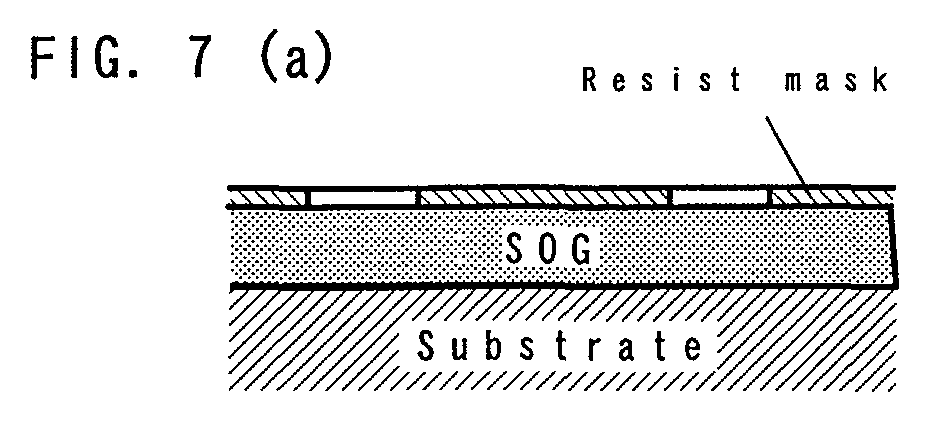
- an intermediate insulating film being comprised of SiO 2 deposited through a CVD method or of SOG and having a low dielectric constant, is formed on a substrate, and a resist mask having a pattern is provided thereon.
- a resist mask having a pattern is provided thereon.
- trench pattern is formed.
- the trench pattern is lined with barrier metal, and as shown in Fig. 7 (d), Cu is embedded into the trench by means of electrolysis plating so as to form a lower layer wiring.
- another intermediate insulating film is formed thereon as shown in Fig. 7 (e).
- via-holes or contact holes
- trench holes i.e., gutters for an upper layer wiring
- dual damascene As shown in Fig. 7 (g), the via-holes and the trench-holes for an upper layer wiring are lined with barrier metal and, as shown in Fig. 7 (h), Cu is embedded into the via-holes and the trench-holes for an upper layer wiring by means of electrolysis plating or the like, and thereby an upper layer wiring is formed.
- copper is used for forming wiring in a damascene method.
- a damascene method forming can be conducted with aluminum.
- the present invention can be applied to a damascene method using various conductive metals as alternatives to copper.
- organic or inorganic SOG having a lower dielectric constant has been examined as a means of overcoming this drawback. Further, it is desired to make organic or inorganic SOG having a lower dielectric constant.
- the dielectric constant of an intermediate insulating film can be decreased by making the intermediate insulating film porous.
- the lower dielectric constant of such an intermediate insulating film corresponds to a decrease in the density of the film.
- alteration or corrosion occurs in the surface of the intermediate insulating film when wet stripping of a resist film is conducted as a subsequent process, and thus it is difficult to obtain a reliable semiconductor element thereby.
- Si-R group (R refers to lower alkyl group or hydrogen atom) is decomposed (R group is separated) by the wet stripping process and a Si-OH bond is produced.
- Si-CH 3 bond (CH 3 is an example) is broken to be Si-OH.
- Si-H bond is broken to be Si-OH.
- Japanese Patent Application Publication Hei 11-162969 discloses that a lower SOG layer is formed, plasma processing using inert gas such as Ar, Kr, Ne, N 2 , He or the like is conducted to the lower SOG layer, and thereby the adherence with respect to an upper SOG layer is increased.
- Japanese Patent Application Publication Hei 11-40813 discloses that plasma processing using low reactivity gas such as N 2 , Ar, He, O 2 or the like is conducted to the surface of a semiconductor element in which a contact region is formed by a dry etching process, residual etching gas or a reaction product is removed, and defect in the semiconductor element is reduced.
- Japanese Patent Application Publication 2000-352827 discloses that a silicon nitride film is formed on a substrate, an etching process is conducted to the silicon nitride film through a photoresist mask, plasma processing is conducted using hydrogen, ammonia, nitrogen, inert gas, or mixed gas thereof, and thereafter a cured surface layer of the photoresist mask is removed by a wet process.
- a method for processing a coating film comprising the steps of forming a silica group coating film having a dielectric constant equal to or less than 2.7 on a substrate, conducting an etching process to the silica group coating film through a photoresist pattern, processing the silica group coating film, to which an etching process has been conducted, with plasma induced from helium gas, and removing the photoresist pattern by a wet stripping process.
- the dielectric constant equal to or less than 2.7 is preferable for an intermediate insulating film used in a damascene method.
- the silica group coating film is not limited to a particular one as long as it has such a dielectric constant.
- the silica group coating film having such a dielectric constant can be achieved by forming with coating liquid as follows:
- the coating liquid can include a condensation product which is obtained through hydrolysis of trialkoxysilane within an organic solvent under an acid catalysis.
- a condensation product which is obtained through hydrolysis of trialkoxysilane within an organic solvent under an acid catalysis.
- An intermediate insulating film having a ladder structure can be obtained by using trialkoxysilane having a concentration of 1% - 5% by weight in a case of conversion into SiO 2 .
- a film which is dense and has a low dielectric constant can preferably be formed.
- trimethoxysilane triethoxysilane, tripropoxysilane, tributoxysilane, diethoxy monomethoxysilane, monomethoxy dipropoxysilane, dibutoxy monomethoxysilane, ethoxy methoxy propoxysilane, monoethoxy dimethoxysilane, monoethoxy dipropoxysilane, butoxy ethoxy propoxysilane, dimethoxy monopropoxysilane, diethoxy monopropoxysilane, and monobutoxy dimethoxysilane.
- trimethoxysilane triethoxysilane
- tripropoxysilane tripropoxysilane
- tributoxysilane trimethoxysilane and triethoxysilane are preferable.
- alkylene glycol dialkyl ether As the solvent, in order to increase the stability of preservation, it is necessary to use alkylene glycol dialkyl ether. By using this, it is possible to control a decomposition reaction of a H-Si group in trialkoxysilane or a substitution reaction of a hydroxy group for an alkoxy group in silanol produced as an intermediate product, which occurs in the conventional art using lower alcohol as a solvent, and thereby it is possible to prevent the gelation.
- alkylene glycol dialkyl ether As the alkylene glycol dialkyl ether, it is possible to list a dialkylether type of alkylene glycol such as ethylene glycol dimethylether, ethylene glycol diethylether, ethylene glycol dipropylether, ethylene glycol dibutylether, diethylene glycol dimethylether, diethylene glycol diethylether, diethylene glycol dipropylether, diethylene glycol dibutylether, propylene glycol dimethylether, propylene glycol diethylether, propylene glycol dipropylether, and propylene glycol dibutylether.
- a preferable compound is a dialkylether type, in particular, dimethylether of ethylene glycol or propylene glycol.
- These organic solvents may be used alone or by combining two or more kinds thereof. Also, these organic solvents are used at a ratio of 10 - 30 times mol with respect to 1 mol of alkoxysilane.
- water used for hydrolysis of trialkoxysilane be within a range of 2.5 - 3.0 mols with respect to 1 mol of trialkoxysilane, preferably within a range of 2.8 - 3.0 mols, so as to increase the degree of hydrolysis. If it is beneath this range, although the stability in preservation is increased, the degree of hydrolysis is deteriorated, the content of organic groups in the hydrolysis product is increased, and thereby gas is generated at the time of forming a coating film. If it is above this range, the stability in preservation is deteriorated.
- the coating liquid obtained in this manner has characteristics of showing the increase in the weight of the film-forming component after the removal of the solvent in a thermogravimetric analysis, and not having a peak at 3,000 cm -1 in the infrared absorption spectrum.
- the conventional coating liquid which is described in Japanese unexamined patent application publication No. Hei 4-216827 (1992), shows a decrease in the weight in a thermogravimetric analysis, and has a peak in the vicinity of 3,000 cm -1 in the infrared absorption spectrum, which indicates that alkoxy group still exists therein.
- One kind selected from polyalkylene glycol and the end alkylation product thereof may be included in the coating liquid.
- an intermediate insulating film can be made porous and the dielectric constant can be decreased.
- polyalkylene glycol As the polyalkylene glycol, it is possible to list lower polyalkylene glycol such as polyethylene glycol, polypropylene glycol or the like.
- the end alkylation product means lower polyalkylene glycol in which a hydroxy group in one or both end(s) of the lower polyalkylene glycol is made to be alkoxyl with a lower alkyl group such as a methyl group, an ethyl group, a propyl group, or the like.
- the addition amount of the one kind selected from polyalkylene glycol and the end alkylation product is 10% - 500% by weight, preferably 50% - 200% by weight, with respect to the solid component of the coating liquid.
- the weight-average molecular weight of the polyalkylene glycol and the end alkylation product is 100 - 10,000, preferably 200 - 5,000. This range can easily make the dielectric constant lower without any damage to solubility in the coating liquid.
- an amine group stripping solution including an amine group such as hydroxylamine, a hydrofluoric acid group stripping solution including ammonium fluoride, or a stripping solution of a mixed group thereof can be used.
- a stripping solution for photoresist which is selected from the above-mentioned groups can be used in the wet stripping process of the present invention.
- a method for manufacturing a semiconductor element comprising the following steps of:
- a silica group coating film for example, coating liquid is applied onto a substrate such as a semiconductor substrate, a glass substrate, a metal plate, a ceramic substrate, or the like by means of a spinner method, a roll coater method, an immersion coating method, a spray method, a screen printing method, a brush painting method, or the like. It is dried to evaporate the solvent therein, fired in a temperature of 250 - 500°C, and a coating film is formed.
- a plasma processing apparatus for generating plasma gas from the above-mentioned gas for example, TCA-7822 manufactured by Tokyo Ohka Kogyo Co., Ltd.
- the plasma processing is conducted under pressure of 10- 600 mTorr, preferably 100 - 500 mTorr, and for 30 - 300 seconds, preferably 30 - 120 seconds.
- Another plasma processing apparatus may be used besides the TCA-7822.
- Triethoxysilane of 73.9 g (0.45 mol) having a concentration of 3% by weight in a case of conversion into SiO 2 is dissolved and stirred into ethylene glycol dimethylether of 799.0 g (8.87 mol), a mixture of pure water of 24.2 g (1.34 mol) and strong nitric acid of 5 ppm is slowly stirred and dropped thereinto, and it is stirred for about 3 hours. Thereafter, it is left still for 6 days at room temperature, so as to obtain a solution.
- Reduced-pressure distillation is conducted to this solution at 120 - 140 mmHg and 40 °C for 1 hour, and a solution in which the concentration of solid component is 8% by weight and the concentration of ethanol is 3% by weight is prepared.
- a both-end methylation product of polyethylene glycol having weight-average molecular weight of 200 is added to this solution at a ratio of 100% by weight to the solid component, is sufficiently stirred, and thereby a uniform solution is obtained.
- This solution is a coating liquid.
- a substrate is rotated and coated with this coating liquid, and thereby a coating film having a thickness of 4500 ⁇ and a refractive index of 1.40 is formed on the substrate.
- Plasma processing is conducted with helium gas having a concentration of 700 sccm at the pressure of 500 mTorr for 30 seconds.
- a wet stripping process is conducted with an amine group stripping solution for photoresist (SST-3 manufactured by Tokyo Ohka Kogyo Co., Ltd.) through immersion at 80 °C for 10 minutes.
- SST-3 manufactured by Tokyo Ohka Kogyo Co., Ltd.
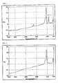
- a SOG layer in this instance is observed by an IR measurement. As shown in FIG. 1, the Si-H bond is left and no alteration in the surface is recognized. Also, the photoresist film and the residue after the etching process is completely removed.
- a SOG layer in this instanse is observed by an IR measurement. As shown in FIG. 3, the Si-H bond is left and no alteration in the surface is recognized. Also, the photoresist film and the residue after the etching process is completely removed.
- a wet stripping process is conducted with a stripping solution for photoresist which is obtained by mixing amine with a hydrofluoric acid group stripping solution (SST-A7 manufactured by Tokyo Ohka Kogyo Co., Ltd.) at 25 °C for 10 minutes.
- a stripping solution for photoresist which is obtained by mixing amine with a hydrofluoric acid group stripping solution (SST-A7 manufactured by Tokyo Ohka Kogyo Co., Ltd.) at 25 °C for 10 minutes.
- a SOG layer in this instance is observed by an IR measurement. As shown in FIG. 5, the Si-H bond is left and no alteration in the surface is recognized. Also, the photoresist film and the residue after the etching process is completely removed.
- the IR measurement indicates that the Si-H bond is broken down. As a result of this, the k value of the SOG layer becomes high, whereby the insulating property thereof is deteriorated. Also, the Si-H bond is transformed into a Si-OH bond which can cause trouble such as degas in a subsequent process of forming a multi-layer structure.
- the silica group coating film since an etching process is conducted to a silica group coating film having a dielectric constant equal to or less than 2.7 formed on a substrate through a photoresist pattern, and thereafter, plasma processing is conducted to the silica group coating film with plasma induced from helium gas, the silica group coating film is not damaged when a wet stripping process is conducted to the photoresist pattern as a subsequent process, and the low dielectric constant can be maintained.
- the present invention is applied to the damascene method, it is possible to obtain a reliable semiconductor element.
- the dielectric constant of the silica group coating film formed with the coating liquid can be lowered, which is advantageous to a fine product.
Landscapes
- Internal Circuitry In Semiconductor Integrated Circuit Devices (AREA)
- Formation Of Insulating Films (AREA)
- Drying Of Semiconductors (AREA)
Abstract
Description
Claims (4)
- A method for processing a coating film comprising the steps of:forming a silica group coating film having a dielectric constant equal to or less than 2.7 on a substrate;conducting an etching process to said silica group coating film through a photoresist pattern;processing said silica group coating film, to which said etching process has been conducted, with plasma induced from helium gas; andconducting a wet stripping process to said photoesist pattern.
- A method for processing a coating film as defined in claim 1, wherein a coating liquid for forming said silica group coating film includes one kind selected from polyalkylene glycol and the end alkylation product thereof.
- A method for processing a coating film as defined in claim 1 or claim 2, wherein a stripping solution for said wet stripping process has a composition including at least an ammonium fluoride compound and/or an alkanolamine compound.
- A method for manufacturing a semiconductor element comprising the following steps of:(1) forming a silica group coating film having a dielectric constant equal to or less than 2.7 on a substrate;(2) providing a photoresist pattern on said silica group coating film;(3) conducting an etching process to said silica group coating film using said photoresist pattern as a mask;(4) processing said silica group coating film with plasma induced from helium gas; and(5) conducting a wet stripping process to said photoresist pattern.
Applications Claiming Priority (2)
| Application Number | Priority Date | Filing Date | Title |
|---|---|---|---|
| JP2001133785A JP4124315B2 (en) | 2001-05-01 | 2001-05-01 | Coating method and method for manufacturing semiconductor device using the method |
| JP2001133785 | 2001-05-01 |
Publications (3)
| Publication Number | Publication Date |
|---|---|
| EP1255289A2 true EP1255289A2 (en) | 2002-11-06 |
| EP1255289A3 EP1255289A3 (en) | 2003-12-03 |
| EP1255289B1 EP1255289B1 (en) | 2007-08-08 |
Family
ID=18981585
Family Applications (1)
| Application Number | Title | Priority Date | Filing Date |
|---|---|---|---|
| EP02253086A Expired - Lifetime EP1255289B1 (en) | 2001-05-01 | 2002-05-01 | Method for processing a coating film and method for manufacturing a semiconductor element with use of the same method |
Country Status (6)
| Country | Link |
|---|---|
| US (1) | US6746963B2 (en) |
| EP (1) | EP1255289B1 (en) |
| JP (1) | JP4124315B2 (en) |
| KR (1) | KR100835659B1 (en) |
| CN (1) | CN1245743C (en) |
| TW (1) | TW558770B (en) |
Families Citing this family (1)
| Publication number | Priority date | Publication date | Assignee | Title |
|---|---|---|---|---|
| JP4358563B2 (en) * | 2003-07-02 | 2009-11-04 | 東京エレクトロン株式会社 | Method for forming low dielectric constant insulating film of semiconductor device |
Family Cites Families (16)
| Publication number | Priority date | Publication date | Assignee | Title |
|---|---|---|---|---|
| US4165295A (en) * | 1976-10-04 | 1979-08-21 | Allied Chemical Corporation | Organic stripping compositions and method for using same |
| JP3214186B2 (en) * | 1993-10-07 | 2001-10-02 | 三菱電機株式会社 | Method for manufacturing semiconductor device |
| KR19980057054A (en) * | 1996-12-30 | 1998-09-25 | 김영환 | Via hole formation method of semiconductor device |
| JP3416472B2 (en) | 1997-07-15 | 2003-06-16 | シャープ株式会社 | Semiconductor element |
| KR100212534B1 (en) | 1997-08-12 | 1999-08-02 | 이서봉 | The sol-gel composition and is manufactured from which the polymer ion conductive membrane |
| JPH11162969A (en) | 1997-11-28 | 1999-06-18 | Seiko Epson Corp | Method for manufacturing semiconductor device |
| JP3177968B2 (en) | 1998-12-04 | 2001-06-18 | 日本電気株式会社 | Semiconductor device and manufacturing method thereof |
| US6387819B1 (en) * | 1998-04-29 | 2002-05-14 | Applied Materials, Inc. | Method for etching low K dielectric layers |
| US6395651B1 (en) * | 1998-07-07 | 2002-05-28 | Alliedsignal | Simplified process for producing nanoporous silica |
| JP2000174121A (en) | 1998-12-04 | 2000-06-23 | Matsushita Electronics Industry Corp | Semiconductor device and manufacture thereof |
| JP3328250B2 (en) | 1998-12-09 | 2002-09-24 | 岸本産業株式会社 | Resist residue remover |
| US6413882B1 (en) * | 1999-04-14 | 2002-07-02 | Alliedsignal Inc. | Low dielectric foam dielectric formed from polymer decomposition |
| JP3287406B2 (en) | 1999-06-11 | 2002-06-04 | 日本電気株式会社 | Method for manufacturing semiconductor device |
| EP1077479A1 (en) | 1999-08-17 | 2001-02-21 | Applied Materials, Inc. | Post-deposition treatment to enchance properties of Si-O-C low K film |
| US6346489B1 (en) | 1999-09-02 | 2002-02-12 | Applied Materials, Inc. | Precleaning process for metal plug that minimizes damage to low-κ dielectric |
| EP1094506A3 (en) | 1999-10-18 | 2004-03-03 | Applied Materials, Inc. | Capping layer for extreme low dielectric constant films |
-
2001
- 2001-05-01 JP JP2001133785A patent/JP4124315B2/en not_active Expired - Fee Related
-
2002
- 2002-04-30 CN CNB021215286A patent/CN1245743C/en not_active Expired - Fee Related
- 2002-04-30 TW TW091109013A patent/TW558770B/en not_active IP Right Cessation
- 2002-04-30 US US10/136,744 patent/US6746963B2/en not_active Expired - Lifetime
- 2002-04-30 KR KR1020020023603A patent/KR100835659B1/en not_active Expired - Fee Related
- 2002-05-01 EP EP02253086A patent/EP1255289B1/en not_active Expired - Lifetime
Also Published As
| Publication number | Publication date |
|---|---|
| US20020164886A1 (en) | 2002-11-07 |
| KR100835659B1 (en) | 2008-06-09 |
| EP1255289B1 (en) | 2007-08-08 |
| KR20020084697A (en) | 2002-11-09 |
| CN1389907A (en) | 2003-01-08 |
| TW558770B (en) | 2003-10-21 |
| CN1245743C (en) | 2006-03-15 |
| US6746963B2 (en) | 2004-06-08 |
| JP2002329782A (en) | 2002-11-15 |
| JP4124315B2 (en) | 2008-07-23 |
| EP1255289A3 (en) | 2003-12-03 |
Similar Documents
| Publication | Publication Date | Title |
|---|---|---|
| US6509279B2 (en) | Methods for processing a coating film and for manufacturing a semiconductor element | |
| US7179758B2 (en) | Recovery of hydrophobicity of low-k and ultra low-k organosilicate films used as inter metal dielectrics | |
| US8445075B2 (en) | Method to minimize wet etch undercuts and provide pore sealing of extreme low k (k<2.5) dielectrics | |
| WO2006049595A1 (en) | Recovery of hydrophobicity of low-k and ultra low-k organosilicate films used as inter metal dielectrics | |
| US6767839B1 (en) | Method for forming multi-layer wiring structure | |
| KR100739082B1 (en) | Method For Forming Coating Film | |
| US20050136687A1 (en) | Porous silica dielectric having improved etch selectivity towards inorganic anti-reflective coating materials for integrated circuit applications, and methods of manufacture | |
| EP1255289B1 (en) | Method for processing a coating film and method for manufacturing a semiconductor element with use of the same method | |
| US6995096B2 (en) | Method for forming multi-layer wiring structure | |
| US7601396B2 (en) | Coating film forming method | |
| JP2002043422A (en) | Method for processing film and method for manufacturing semiconductor device using the same | |
| JP2002319582A (en) | Coating liquid for forming silica based coating | |
| EP0535677B1 (en) | Insulation layer forming method | |
| JP2004006890A (en) | Method for forming multi-layered wiring structure | |
| KR20050041909A (en) | Method for forming silica-based processed film resistant to washing, and silica-based processed film resistant to washing obtained by the method |
Legal Events
| Date | Code | Title | Description |
|---|---|---|---|
| PUAI | Public reference made under article 153(3) epc to a published international application that has entered the european phase |
Free format text: ORIGINAL CODE: 0009012 |
|
| AK | Designated contracting states |
Kind code of ref document: A2 Designated state(s): AT BE CH CY DE DK ES FI FR GB GR IE IT LI LU MC NL PT SE TR |
|
| AX | Request for extension of the european patent |
Free format text: AL;LT;LV;MK;RO;SI |
|
| PUAL | Search report despatched |
Free format text: ORIGINAL CODE: 0009013 |
|
| AK | Designated contracting states |
Kind code of ref document: A3 Designated state(s): AT BE CH CY DE DK ES FI FR GB GR IE IT LI LU MC NL PT SE TR |
|
| AX | Request for extension of the european patent |
Extension state: AL LT LV MK RO SI |
|
| RIC1 | Information provided on ipc code assigned before grant |
Ipc: 7H 01L 21/768 B Ipc: 7H 01L 21/311 B Ipc: 7H 01L 21/316 A |
|
| 17P | Request for examination filed |
Effective date: 20040506 |
|
| 17Q | First examination report despatched |
Effective date: 20040617 |
|
| AKX | Designation fees paid |
Designated state(s): BE FR IT |
|
| REG | Reference to a national code |
Ref country code: DE Ref legal event code: 8566 |
|
| GRAP | Despatch of communication of intention to grant a patent |
Free format text: ORIGINAL CODE: EPIDOSNIGR1 |
|
| GRAS | Grant fee paid |
Free format text: ORIGINAL CODE: EPIDOSNIGR3 |
|
| GRAA | (expected) grant |
Free format text: ORIGINAL CODE: 0009210 |
|
| AK | Designated contracting states |
Kind code of ref document: B1 Designated state(s): BE FR IT |
|
| ET | Fr: translation filed | ||
| PLBE | No opposition filed within time limit |
Free format text: ORIGINAL CODE: 0009261 |
|
| STAA | Information on the status of an ep patent application or granted ep patent |
Free format text: STATUS: NO OPPOSITION FILED WITHIN TIME LIMIT |
|
| 26N | No opposition filed |
Effective date: 20080509 |
|
| PGFP | Annual fee paid to national office [announced via postgrant information from national office to epo] |
Ref country code: BE Payment date: 20080520 Year of fee payment: 7 |
|
| BERE | Be: lapsed |
Owner name: TOKYO OHKA KOGYO CO., LTD. Effective date: 20090531 |
|
| PG25 | Lapsed in a contracting state [announced via postgrant information from national office to epo] |
Ref country code: BE Free format text: LAPSE BECAUSE OF NON-PAYMENT OF DUE FEES Effective date: 20090531 |
|
| REG | Reference to a national code |
Ref country code: FR Ref legal event code: PLFP Year of fee payment: 15 |
|
| REG | Reference to a national code |
Ref country code: FR Ref legal event code: PLFP Year of fee payment: 16 |
|
| REG | Reference to a national code |
Ref country code: FR Ref legal event code: PLFP Year of fee payment: 17 |
|
| PGFP | Annual fee paid to national office [announced via postgrant information from national office to epo] |
Ref country code: FR Payment date: 20210412 Year of fee payment: 20 Ref country code: IT Payment date: 20210412 Year of fee payment: 20 |