EP1255286A1 - Monitor, method of monitoring, polishing device, and method of manufacturing semiconductor wafer - Google Patents
Monitor, method of monitoring, polishing device, and method of manufacturing semiconductor wafer Download PDFInfo
- Publication number
- EP1255286A1 EP1255286A1 EP00981828A EP00981828A EP1255286A1 EP 1255286 A1 EP1255286 A1 EP 1255286A1 EP 00981828 A EP00981828 A EP 00981828A EP 00981828 A EP00981828 A EP 00981828A EP 1255286 A1 EP1255286 A1 EP 1255286A1
- Authority
- EP
- European Patent Office
- Prior art keywords
- mentioned
- light
- optical fiber
- monitoring device
- polishing
- Prior art date
- Legal status (The legal status is an assumption and is not a legal conclusion. Google has not performed a legal analysis and makes no representation as to the accuracy of the status listed.)
- Withdrawn
Links
Images




Classifications
-
- H—ELECTRICITY
- H10—SEMICONDUCTOR DEVICES; ELECTRIC SOLID-STATE DEVICES NOT OTHERWISE PROVIDED FOR
- H10P—GENERIC PROCESSES OR APPARATUS FOR THE MANUFACTURE OR TREATMENT OF DEVICES COVERED BY CLASS H10
- H10P74/00—Testing or measuring during manufacture or treatment of wafers, substrates or devices
-
- B—PERFORMING OPERATIONS; TRANSPORTING
- B24—GRINDING; POLISHING
- B24B—MACHINES, DEVICES, OR PROCESSES FOR GRINDING OR POLISHING; DRESSING OR CONDITIONING OF ABRADING SURFACES; FEEDING OF GRINDING, POLISHING, OR LAPPING AGENTS
- B24B37/00—Lapping machines or devices; Accessories
- B24B37/005—Control means for lapping machines or devices
- B24B37/013—Devices or means for detecting lapping completion
-
- B—PERFORMING OPERATIONS; TRANSPORTING
- B24—GRINDING; POLISHING
- B24B—MACHINES, DEVICES, OR PROCESSES FOR GRINDING OR POLISHING; DRESSING OR CONDITIONING OF ABRADING SURFACES; FEEDING OF GRINDING, POLISHING, OR LAPPING AGENTS
- B24B49/00—Measuring or gauging equipment for controlling the feed movement of the grinding tool or work; Arrangements of indicating or measuring equipment, e.g. for indicating the start of the grinding operation
- B24B49/02—Measuring or gauging equipment for controlling the feed movement of the grinding tool or work; Arrangements of indicating or measuring equipment, e.g. for indicating the start of the grinding operation according to the instantaneous size and required size of the workpiece acted upon, the measuring or gauging being continuous or intermittent
- B24B49/04—Measuring or gauging equipment for controlling the feed movement of the grinding tool or work; Arrangements of indicating or measuring equipment, e.g. for indicating the start of the grinding operation according to the instantaneous size and required size of the workpiece acted upon, the measuring or gauging being continuous or intermittent involving measurement of the workpiece at the place of grinding during grinding operation
-
- B—PERFORMING OPERATIONS; TRANSPORTING
- B24—GRINDING; POLISHING
- B24B—MACHINES, DEVICES, OR PROCESSES FOR GRINDING OR POLISHING; DRESSING OR CONDITIONING OF ABRADING SURFACES; FEEDING OF GRINDING, POLISHING, OR LAPPING AGENTS
- B24B49/00—Measuring or gauging equipment for controlling the feed movement of the grinding tool or work; Arrangements of indicating or measuring equipment, e.g. for indicating the start of the grinding operation
- B24B49/12—Measuring or gauging equipment for controlling the feed movement of the grinding tool or work; Arrangements of indicating or measuring equipment, e.g. for indicating the start of the grinding operation involving optical means
-
- B—PERFORMING OPERATIONS; TRANSPORTING
- B24—GRINDING; POLISHING
- B24D—TOOLS FOR GRINDING, BUFFING OR SHARPENING
- B24D7/00—Bonded abrasive wheels, or wheels with inserted abrasive blocks, designed for acting otherwise than only by their periphery, e.g. by the front face; Bushings or mountings therefor
- B24D7/12—Bonded abrasive wheels, or wheels with inserted abrasive blocks, designed for acting otherwise than only by their periphery, e.g. by the front face; Bushings or mountings therefor with apertures for inspecting the surface to be abraded
Definitions
- NA numerical aperture
- Measurement of the residual film thickness in polishing and ascertainment of the endpoint of the process are among the most important performance requirements in such a substrate polishing apparatus.
- the precision of this measurement greatly influences the quality of the semiconductor elements that are manufactured by means of this apparatus, and therefore the quality of the integrated circuits.
- polishing apparatuses are all on an extension of existing apparatuses, and cannot currently satisfy requirements for an increased degree of working precision.
- fluctuating factors in the amount of polishing per unit time e.g., various factors that fluctuate on an occasional basis such as the polishing pressure, amount of polishing agent supplied and temperature environment of the substrate, etc., in addition to clogging of polishing pad, cannot be handled in the case of control methods that depend on the setting of the working time.
- detection methods that utilize fluctuations in the torque of the motor that drives the polishing surface plate have been proposed as detection methods for detecting the polish ing endpoint at the same time that polishing is performed (i.e., in-situ).
- detection methods utilize the fact that the polishing resistance varies when the material of the polished surface of the substrate varies at the polishing endpoint. Fluctuations in the polishing resistance are detected by monitoring the motor torque, and the polishing endpoint is detected from variations in the motor torque.
- the monitoring device 109 must be fastened to the rotating polishing surface plate 104. Since the monitoring device is equipped with a light source and a photo-detector, an accommodating space of a size that cannot be ignored is required in the lower part of the polishing surface plate 104 in order to accommodate this monitoring device in cases where the monitoring device rotates. This greatly restricts the design of the CMP polishing apparatus.
- One object of the present invention is to solve the above-mentioned problems, and to provide a monitoring device and monitoring method that make it possible to measure the residual film thickness with a high degree of precision, and to detect the process endpoint by optical means, regardless of the actual material of the substrate.
- Another object of the present invention is to provide a compact, light-weight polishing apparatus which is equipped with this monitoring device and which is capable of high-precision polishing.
- Still another object of the present invention is to provide a method for polishing and manufacturing semiconductor wafers with a high degree of precision using this polishing apparatus.
- the first invention that is used in order to achieve the above-mentioned objects is a monitoring device which is equipped with a polishing body part that has a rotatable polishing body with a working surface, and a substrate holding part that holds a substrate, and which monitors the polishing conditions by means of a reflected signal light obtained by illuminating the polished surface of the above-mentioned substrate with probe light when this polished surface is polished by interposing a polishing agent between the above-mentioned rotating working surface and this polished surface, and producing a relative motion between these two parts
- this monitoring device being characterized by the fact that the device is equipped with a non-rotating light source which emits the above-mentioned probe light, a non-rotating light detector which receives the above-mentioned reflected signal light, and a turnabout optical part which emits the above-mentioned reflected signal light from a specified position on the axis of rotation of the above-mentioned polishing body part when the above-mentione
- polishing body part refers not only to the polishing body, polishing surface plate and shaft, but also to the mechanical system equipped with a rotating mechanism, etc.
- the second invention that is used in order to achieve the above-mentioned objects is the above-mentioned first invention which is further characterized by the fact that the above-mentioned turnabout optical part is equipped with a light-coupling lens and a second optical fiber with a refractive index of n 0 , and the above-mentioned monitoring device is further equipped with a non-rotating first optical fiber.
- the third invention that is used in order to achieve the above-mentioned objects is the above-mentioned first invention which is further characterized by the fact that the above-mentioned monitoring device is equipped with a non-rotating first reflective mirror, and the above-mentioned turnabout optical part is equipped with a second reflective mirror and a third reflective mirror.
- the fourth invention that is used in order to achieve the above-mentioned objects is any of the above-mentioned first through third inventions which is further characterized by the fact that the above-mentioned turnabout optical part is equipped with a transparent window having a refractive index of n 1 which transmits the above-mentioned probe light toward the above-mentioned polished surface, and which transmits the above-mentioned reflected signal light in the opposite direction.
- the sixth invention that is used in order to achieve the above-mentioned objects is the above-mentioned fourth invention which is further characterized by the fact that the end portion of the above-mentioned second optical fiber and the above-mentioned transparent window are bonded by an adhesive agent with a refractive index whose difference from n 0 is ⁇ 17% or less, and an anti-reflection film which is used to reduce interfacial reflection between the above-mentioned adhesive agent and the above-mentioned transparent window is formed on at least the bonded portion of the above-mentioned transparent window.
- the seventh invention that is used in order to achieve the above-mentioned objects is the above-mentioned fourth invention which is further characterized by the fact that the above-mentioned turnabout optical part is further equipped with an optical system which is installed between the above-mentioned transparent window and the end surface of the above-mentioned second optical fiber, and which has a convex power that is used to illuminate the above-mentioned polished surface with probe light that is emitted from the above-mentioned end surface of the above-mentioned second optical fiber, and to focus the reflected signal light on the above-mentioned end surface of the above-mentioned second optical fiber.
- the eighth invention that is used in order to achieve the above-mentioned objects is the above-mentioned fourth invention which is further characterized by the fact that the above-mentioned turnabout optical part is further equipped with an optical system which is installed between the above-mentioned transparent window and the above-mentioned third reflective mirror, and which has a convex power that is used to illuminate the above-mentioned polished surface with probe light that is emitted from the above-mentioned third reflective mirror, and to relay the reflected signal light to the above-mentioned third reflective mirror.
- the ninth invention that is used in order to achieve the above-mentioned objects is the above-mentioned seventh invention which is further characterized by the fact that a lens with a refractive index of n 2 which is located closest to the above-mentioned end surface of the above-mentioned second optical fiber in the above-mentioned optical system and the above-mentioned end surface of the above-mentioned second optical fiber are bonded by an adhesive agent with a refractive index whose difference from n 0 is ⁇ 17% or less, and whose difference from n 2 is ⁇ 17% or less.
- the tenth invention that is used in order to achieve the above-mentioned objects is the above-mentioned seventh invention which is further characterized by the fact that a lens with a refractive index of n 2 which is located closest to the above-mentioned end surface of the above-mentioned second optical fiber in the above-mentioned optical system and the above-mentioned end surface of the above-mentioned second optical fiber are bonded by an adhesive agent with a refractive index whose difference from n 0 is ⁇ 17% or less, and an anti-reflection film which is used to reduce interfacial reflection between the above-mentioned adhesive agent and the above-mentioned lens with a refractive index of n 2 is formed on at least the bonded portion of the above-mentioned lens with a refractive index of n 2 .
- the twelfth invention that is used in order to achieve the above-mentioned objects is any of the above-mentioned second, fourth through seventh or ninth through eleventh inventions which is further characterized by the fact that the normal direction of at least one end surface of the above-mentioned first or second optical fiber is set so that this normal direction is not parallel to the direction of the optical axis of the above-mentioned first or second optical fiber.
- the thirteenth invention that is used in order to achieve the above-mentioned objects is any of the above-mentioned second, fourth through seventh or ninth through twelfth inventions which is further characterized by the fact that at least the above-mentioned first or second optical fiber, or both optical fibers, are optical fibers equipped with a core that consists of a liquid.
- the fourteenth invention that is used in order to achieve the above-mentioned objects is a monitoring method which monitors the polishing state by means of a reflected signal light obtained by illuminating the polished surface of a substrate with probe light when this polished surface is polished by interposing a polishing agent between a rotating working surface and this polished surface, and producing a relative motion between these two parts, this monitoring method being characterized by the fact that the method includes a step in which probe light is emitted from a non-rotating light source, a step in which the above-mentioned probe light is caused to be incident on a turnabout optical part which rotates together with the above-mentioned working surface, and a step in which the reflected signal light emitted from the above-mentioned turnabout optical part is received by a non-rotating light detector.
- the fifteenth invention that is used in order to achieve the above-mentioned objects is a polishing apparatus which is characterized by the fact that this apparatus is equipped with the monitoring device of any of the above-mentioned first through thirteenth inventions.
- the sixteenth invention that is used in order to achieve the above-mentioned objects is a semiconductor wafer manufacturing method which is characterized by the fact that the above-mentioned substrate is a semiconductor wafer on which a semiconductor element is formed, and this method includes a step in which the surface of a substrate is polished using the polishing apparatus of the fifteenth invention.
- the compact turnabout optical part i.e., the objective part
- the light source, light detector, beam splitter and spectroscope in the case of a spectroscopic method
- the measuring parts which require a relatively large amount of installation space
- the degree of freedom in the design of a polishing apparatus equipped with this monitoring device is increased, and the size and weight of the apparatus can be reduced.
- the polishing conditions can be monitored with a high degree of precision.
- the monitoring method of the present invention makes it possible not only to monitor the polishing conditions with a high degree of precision, but also to increase the degree of freedom in the design of the polishing apparatus, and to make the polishing apparatus more compact.
- the polishing apparatus of the present invention is not only compact, but allows monitoring of the polishing conditions with a high degree of precision.
- the polishing method of the present invention since the polishing conditions are monitored with a high degree of precision, the quality and yield of substrates such as semiconductor elements that are polished can be greatly improved.
- the first light-coupling lens 63 focuses the probe light and causes this light to be incident on the first end surface of the first optical fiber 62; furthermore, this lens causes the reflected signal light that is emitted from the first end surface of the first optical fiber 62 to be incident on the beam splitter 25.
- the first light-coupling lens 63 be matched with the mode of the first optical fiber 62.
- the first optical fiber 62 and second optical fiber 61 transmit the probe light that is incident from the respective first end surfaces of these optical fibers, and cause this light to be emitted from the second end surfaces; furthermore, these optical fibers transmit the reflected signal light that is incident from the second end surfaces, and cause this light to be emitted from the first end surfaces.
- the second light-coupling lens 64 receives the probe light that is emitted from the second end surface of the first optical fiber 62, and focuses this light so that this light is caused to be incident on the first end surface of the second optical fiber 61; moreover, this second light-coupling lens 64 receives the reflected signal light that is emitted from the first end surface of the second optical fiber 61, and focuses this light so that this light is caused to incident on the second end surface of the first optical fiber 62.
- the second light-coupling lens 64 be matched with the modes of both the first optical fiber 62 and the second optical fiber 61.
- the probe light that is emitted from the second end surface of the second optical fiber 61 passes through the transparent window 23 and is caused to illuminate the polished surface of the substrate 42.
- the reflected signal light that is reflected from this point again passes through the transparent window 23 in the opposite direction, and is incident on the second e nd surface of the second optical fiber 61.
- the first optical fiber 62 can be kept in a non-rotating state; as a result, the light source 24, beam splitter 25, light detector 26 and first light-coupling lens 63, which require installation space, can be installed in non-rotating positions. This reduces the restrictions on the installation space, and is extremely convenient for reducing the size of the polishing apparatus.
- the probe light that is emitted from the light source 24 passes through the beam splitter 25; this light further passes through the first light-coupling lens 63 and first optical fiber 62, and is emitted toward the second light-coupling lens 64 from the end surface of the first optical fiber 62 which is in a specified position. This probe light further passes through the light-coupling lens 64, the second optical fiber 61 and the transparent window 23, and is emitted toward the polished surface of the substrate 42.
- the probe light is caused to illuminate the polished surface of the substrate 42, and a reflected signal is acquired when the transparent window 23 rotates beneath the polished surface.
- this monitoring device is equipped with a rotary joint 35, the monitor ing device can be installed in the rotating part of the polishing apparatus, so that the monitoring device has extremely high all-purpose utility.
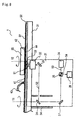
- 21 indicates the monitoring device, which is equipped with a light source 24 that emits probe light, a beam splitter 25, a light detector 26 that receives the reflected signal light, a first reflective mirror 27, a second reflective mirror 28 and a third reflective mirror 29.
- the position on this first reflective mirror 27 from which the probe light is reflected is adjusted so that this position coincides with the specified position for the incidence of the reflected signal light, and is further adjusted so that the reflected probe light coincides with the axis of rotation 11.
- the second reflective mirror 28 and third reflective mirror 29 form a turnabout optical part. If necessary, this turnabout optical part is further equipped with a transparent window 23, and further forms a turnabout optical system together with the polished surface 44.
- the first reflective mirror 27 emits the probe light emitted from the beam splitter 25 toward the second reflective mirror 28, and emits the reflected signal light emitted from the second reflective mirror 28 toward the beam splitter 25.
- the second reflective mirror 28 emits the probe light emitted from the first reflective mirror 27 toward the third reflective mirror 29, and emits the reflected signal light that is reflected and emitted from the third reflective mirror 29 toward the first reflective mirror 27.
- the probe light that is emitted from the third reflective mirror 29 passes through the transparent window 23 and is caused to illuminate the polished surface of the substrate 42.
- the reflected signal light from this point again passes through the transparent window 23 in the opposite direction, strikes the third reflective mirror and is reflected toward the second reflective mirror 28. Then, this light is reflected by the beam splitter 25 (via the first reflective mirror 27), and is incident on the light detector 26, so that this light is detected as a signal.
- the polishing conditions of the polished surface are monitored according to variations in this reflected signal light.
- the first reflective mirror 27, light source 24, beam splitter 25 and light detector 26 can be installed in non-rotating positions, which is extremely convenient for reducing the size of the polishing apparatus.
- the second reflective mirror 28 is built into the interior of the shaft 34, and is arranged so that this second reflective mirror 28 rotates together with the shaft 34.
- the rotating second reflective mirror 28 receives the probe light that is reflected from the non-rotating first reflective mirror 27 while this second reflective mirror 28 rotates, and emits this probe light toward the third reflective mirror 29, which rotates at the same angular velocity as the second reflective mirror 28.
- the rotating second reflective mirror 28 receives (while rotating) the reflected signal light emitted from the third reflective mirror 29 rotating at the same angular velocity as the second reflective mirror 28, and emits this reflected signal light toward the non-rotating first reflective mirror 27.
- the probe light emitted from the light source 24 passes through the beam splitter 25, and is emitted toward the polished surface of the substrate 42 via the first reflective mirror 27 (which is disposed in a specified position), second reflective mirror 28, third reflective mirror 29 and transparent window 23.
- the reflected signal light from this polished surface follows the above-mentioned path in exactly the opposite direction from the probe light; this reflected signal light is reflected by the first reflective mirror 27 (which is disposed in a specified position), and is then reflected by the beam splitter 25, so that this light enters the light detector 26 and is detected.
- the polish ing conditions of the polished surface are monitored according to variations in this reflected signal light.
- the probe light is caused to illuminate the polished surface of the substrate 42, and a reflected signal is acquired when the transparent window 23 rotates beneath the polished surface.
- the present working configuration differs from the first working configuration only in that the end surface of the second optical fiber 61 is bonded to the transparent window 23 using an adhesive agent.
- the probe light emitted from the second optical fiber 61 is caused to illuminate the polished surface of the substrate 42 directly, and the reflected signal light is again caused to be incident on the end surface of the second optical fiber 61.
- the probe light that is emitted from the second optical fiber 61 is divergent light; furthermore, there is a gap between the transparent window and the end surface of the optical fiber, so that the distance between these two parts cannot be ignored. Accordingly, since a considerable amount of the reflected signal light is lost due to divergence, the quantity of light that is incident on the second optical fiber 61 is reduced.
- the end surface of the second optical fiber 61 is bonded to the transparent window 23 using an adhesive agent.
- the end surface of the second optical fiber 61 and the transparent window 23 are bonded using an adhesive agent 70 which has a refractive index that is within the range of no ⁇ 17% and within the range of n 1 ⁇ 17%, where n 0 is the refractive index of the end surface of the second optical fiber, and n 1 is the refractive index of the transparent window 23.
- the present working configuration differs from the third working configuration only in that an anti-reflection film used to reduce the reflectivity at the interface between the adhesive agent and the transparent window is formed on the surface of the transparent window 23.
- the end surface of the second optical fiber 61 and the transparent window 23 are bonded using an adhesive agent 70 which has a refractive index that is within the range of n 0 ⁇ 17% and within the range of n 1 ⁇ 17%, where n 0 is the refractive index of the end surface of the second optical fiber, and n 1 is the refractive index of the transparent window 23.
- an adhesive agent 70 which has a refractive index that is within the range of n 0 ⁇ 17% and within the range of n 1 ⁇ 17%, where n 0 is the refractive index of the end surface of the second optical fiber, and n 1 is the refractive index of the transparent window 23.
- an anti-reflection film which is used to reduce reflection at the interface between the adhesive agent and the transparent window is formed on the surface of the transparent window 23.
- an anti-reflection film (not shown in the figures) is formed on the surface of the transparent window 23 in the third working configuration shown in Figure 3.
- the degree of freedom in the selection of adhesive agents can be increased, and the reflectivity at the two interfaces with the adhesive agent can be sufficiently reduced; consequently, the reflected signal light can be increased.
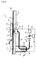
- FIG 4 An overall schematic diagram of the present working configuration is shown in Figure 4, and the optical system in the vicinity of the optical window is shown in Figure 5.
- This working configuration differs from the first working configuration only in that an optical system 22 which has a convex power is disposed between the end surface of the second optical fiber and the transparent window.
- the optical system 22 may also be constructed from a plurality of lenses; in these figures, however, only a single lens is shown in representative terms.
- the reflection loss at the end surface of the second optical fiber 61 and the surface of the transparent window 23 can be reduced by means of the third and fourth working configurations; however, as was described in the third working configuration, the probe light emitted from the second optical fiber is divergent light, and the transparent window 23 has a thickness that cannot be ignored; accordingly, while the probe light and reflected signal light travel over this distance, the light diverges, so that only a portion of the light can enter the end surface of the second optical fiber 61.
- the optical system 22 that has this convex power is designed so that the position of the end surface of the second optical fiber 61 is again optically conjugate with respect to the polished surface of the substrate 42.
- the probe light emitted from the end surface of the second optical fiber 61 is refracted by the optical system 22 having a convex power, and is caused to illuminate the polished surface, and the reflected signal light is again refracted in the opposite direction by the optical system 22 having a convex power.
- an equal-size image of the shape of the end surface at the time of emission is focused on the end surface position of the second optical fiber 61.
- this optical system 22 having a convex power be devised so that the mode is matched with respect to the incidence on and emission from the second optical fiber 61, thus preventing light loss. If this is done, then all of the signal light reflected by the polished surface can in principle be taken into the second optical fiber 61. As a result, the reflected signal light can be increased.
- Figure 6 shows an outline of the optical system of the area in the vicinity of the optical window of the present working configuration.
- This working configuration differs from the fifth working configuration only in that the lens 220 (which is the closest part of the optical system 22 to the end surface of the second optical fiber) and the end surface of the second optical fiber are bonded by means of an adhesive agent 70.
- the optical system 22 is constructed using a plurality of lenses; however, in Figure 6, only a single lens is shown as a representative example in such cases as well.
- n 0 is the refractive index of the end surface of the second optical fiber
- n 2 is the refractive index of the lens 220.
- the interfacial reflection at the end surface of the second optical fiber 61 and the reflection of light by the interface on the bonded surface side of the lens 220 can be reduced; consequently, the reflected signal light can be increased.
- This working configuration differs from the sixth working configuration only in that an anti-reflection film which is used to reduce the reflection at the interface between the adhesive agent and the lens 220 is formed on the surface of the lens 220. Specifically, in Figure 6, an anti-reflection film (not shown in the figures) is formed on the surface of the lens 220.
- the end surface of the second optical fiber 61 and the lens 220 are bonded by means of an adhesive agent 70 which has a refractive index that is within the range of n 0 ⁇ 17% and also within the range of n 2 ⁇ 17%, where n 0 is the refractive index of the end surface of the second optical fiber, and n 2 is the refractive index of the lens 220.
- an adhesive agent 70 which has a refractive index that is within the range of n 0 ⁇ 17% and also within the range of n 2 ⁇ 17%, where n 0 is the refractive index of the end surface of the second optical fiber, and n 2 is the refractive index of the lens 220.
- an anti-reflection film which is used to reduce reflection at the interface between the adhesive agent 70 and the lens 220 is formed on the surface of the lens 220.
- the degree of freedom in the selection of adhesive agents can be increased, and the reflectivity at the two interfaces with the adhesive agent can be sufficiently reduced; consequently, the reflected signal light can be increased.
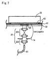
- FIG 7. This working configuration differs from the fifth working configuration only in that the optical system 22 is further developed.
- the optical system 22 is equipped with a front-group optical system 221 and a rear-group optical system 222, and is further equipped with an iris 14.
- the iris 14 is installed in the front-group optical system 221 in a position that is optically conjugate with the polished surface of the substrate 42.
- the direction in which light is emitted from the second optical fiber 61 may vary if there is a bend, etc., in the optical fiber. Consequently, in the case of the monitoring device of the fifth working configuration, the position illuminated by the light may undergo a shift, etc., thus causing measurement error.
- the iris 14 installed in the optical system 22 is installed in order to adjust the light beam from the second optical fiber 61. For this reason, the size of the aperture part of the iris 14 is set so that this size is slightly smaller than the size of the light beam emitted from the optical fiber 61.
- the direction and size of the light beam that passes through this iris 14 can be stabilized even if there is some variation in the direction of the light beam of the probe light that is emitted from the second optical fiber 61. Accordingly, the position on the polished surface of the substrate 42 that is illuminated by the probe light can be fixed along with the illumination range. Furthermore, the shape and dimensions of the illuminated spot on the polished surface can be adjusted by varying the shape and dimensions of this iris. Accordingly, the shape and dimensions of the illuminated spot can be matched to the pattern of the semiconductor device that is the object of measurement. Furthermore, if such an iris 14 is installed, the iris 4 shown in Figures 1,3 and 4 may be omitted.
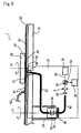
- FIG 8. A schematic diagram of this working configuration is shown in Figure 8.
- This working configuration differs from the second working configuration only in that an optical system 22 which has a convex power is disposed between the third reflective mirror 29 and the transparent window 23.
- the optical system 22 may also be constructed from a plurality of lenses; in this figure, however, this optical system is simply indicated by a square block.
- the probe light emitted from the light source 24 may diverge before reaching the polished surface of the substrate 42, so that the polished surface cannot be illuminated with a spot of the required size. Accordingly, the light is stopped down to a spot of the desired size by means of this optical system 22 with a convex power.
- a relay optical system may be separately installed between the first reflective mirror and the second reflective mirror, or between the second reflective mirror and the third reflective mirror. In this way, it is possible not only to handle diverse semiconductor device patterns, but also to prevent the reflected signal light from straying from the light path of the optical system, so that the light can be received by the light detector 26 without any waste.
- the beam splitter 25, light source 24, optical system including a spectroscope (in cases where a spectroscopic reflected signal is detected), and light detector which require a relatively large installation space, can be installed separately from the polishing apparatus. Furthermore, on the side of the polishing apparatus, it is necessary to install only a compact turnabout optical part equipped with optical fibers, reflective mirrors or lenses, etc., used to achieve the stable transmission of the probe light and illumination of the polished surface with this probe light, and also used for the stable reception of the reflected signal light and the stable transmission of this light to a specified position on the axis of rotation.
- this monitoring device is used in a polishing apparatus, the polishing conditions can be monitored with a high degree of precision without increasing the size of the polishing apparatus. Furthermore, this monitoring method also makes it possible to monitor the polishing conditions with a high degree of precision without increasing the size of the polishing apparatus. Moreover, the polishing apparatus into which this monitoring device is incorporated is compact and light-weight, and can monitor the polishing conditions with a high degree of precision. If this polishing apparatus is used to polish semiconductor wafers on which semiconductor elements are formed, semiconductor wafers can be obtained in which the polishing conditions are monitored with a high degree of precision.
- the reflection of light at the end surfaces of the optical fibers was sometimes a problem.
- the reflected probe light that is reflected by the first end surface and second end surface of the first optical fiber, and by the first end surface and second end surface of the second optical fiber is propagated in the opposite direction from the direction of the substrate 42, and may enter the light detector as noise light (flare light).
- the reflectivity at the respective end surfaces is approximately 3.4%. Since the intensity of the probe light and reflected signal light may drop greatly as a result of scattering loss caused by the polishing agent 41 and loss during propagation by other optical systems, or as a result of the low reflectivity characteristics of certain types of wafers, the intensity of the reflected signal light that finally enters the light detector 26 may be greatly reduced from the intensity of the probe light in the stage of propagation through the optical fibers. Accordingly, a reflectivity of 4% is a value that cannot be ignored.
- this noise light causes a drop in the S/N ratio of the signal, such noise light may cause a deterioration in the measurement precision of the measurement of the polishing conditions, such as the measurement of the residual film thickness and the detection of the polishing endpoint.
- the present working configuration was devised in order to solve the above-mentioned problems, and is a modification of the first, third, fourth, fifth, sixth, seventh and eighth working configurations.
- the difference of the present working configuration from these working configurations lies in the orientation of the end surfaces of the optical fibers.
- the first working configuration there was no stipulation regarding the orientation of the end surfaces of the optical fibers with respect to the direction of the optical axis of the optical fibers.
- the normal directions of the end surfaces of the optical fibers are set so that these normal directions are not parallel to the directions of the optical axes of the optical fibers.
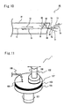
- Figures 9 and 10 are schematic diagrams of one example of the present working configuration.
- Figure 9 differs from the working configuration shown in Figure 1 only in that the end portion 65 of the second optical fiber 61 in Figure 1 (which illustrates the first working configuration) is formed with a wedge shape, and in this end portion 65, the axis of the second optical fiber is set so that this axis is not parallel to the normal direction of the substrate.
- Figure 10 is an enlarged view of the end portion 65 of the second optical fiber 61 shown in Figure 9.
- 61 indicates the second optical fiber, and 71 indicates the axis of this optical fiber; the probe light and reflected signal light are propagated along this axis.
- 72 indicates the direction of propagation of the probe light, and 75 indicates the direction of propagation of the reflected signal light.
- 76 indicates the optical axis of the emitted probe light that is emitted from the second optical fiber 61 and the reflected signal light that is incident on the second optical fiber 61.
- 73 indicates the direction of propagation of the emitted probe light, and 74 indicates the direction of propagation of the reflected signal light.
- 77 indicates the normal direction of the second end surface 73
- 78 indicates the angle of inclination (wedge angle) of the end surface; this is the angle formed by the axis 71 of the optical fiber and the normal direction 80 of the second end surface 80.
- the angle of inclination 78 is set at 8 degrees. Since this angle is also equal to the angle of incidence of the probe light on the second end surface 80, this angle is sometimes also called the "angle of incidence.” Furthermore, since this angle is also equal to the angle of refraction of the reflected signal light with respect to the second end surface, this angle is sometimes also called the "angle of refraction.”
- 81 is the angle corresponding to the angle of refraction when the emitted probe light is emitted, and is an angle of 11.6 degrees. Furthermore, 82 is the angle of reflection when the probe light is reflected by the second end surface 80, and is equal to the angle of incidence 78.
- 83 is the direction of the reflected probe light.
- the description of the probe light up to the point where the probe light reaches the second optical fiber is the same as in the case of the first working configuration; accordingly, this description is omitted here.
- the probe light that is propagated in the direction 72 along the axis 71 of the second optical fiber 61 is incident on the second end surface 80 at the angle of incidence 78; this light is refracted by the angle of refraction 81 and emitted; furthermore, a portion of the probe light is reflected at the angle of reflection 82.
- the refracted probe light is propagated in the direction 73, and is incident on the polished surface of the substrate 42.
- the reflected signal light that is reflected from this point is propagated in the direction 74 along the optical axis 76; this light is incident on the second optical fiber at the second end surface 80 at the angle of incidence 81 and angle of refraction 78, and is propagated in the direction 75 along the axis 71.
- the reflected probe light that is reflected in the direction 83 is inclined by the large angle of 16 degrees with respect to the axis 71 of the optical fiber; accordingly, this light does not form the propagation mode of this second optical fiber, but is radiated and lost during propagation through the second optical fiber 61.
- the monitoring device of the present invention be covered by a pipe, etc., whose interior is coated with a matte light-absorbing coating material, etc., so that no harmful external light enters the light path (e.g., the light path 52, optical system 22 or measuring parts, etc.) and has a deleterious effect on measurements.
Landscapes
- Engineering & Computer Science (AREA)
- Mechanical Engineering (AREA)
- Mechanical Treatment Of Semiconductor (AREA)
- Length Measuring Devices By Optical Means (AREA)
- Constituent Portions Of Griding Lathes, Driving, Sensing And Control (AREA)
- Finish Polishing, Edge Sharpening, And Grinding By Specific Grinding Devices (AREA)
- Optical Couplings Of Light Guides (AREA)
Abstract
Description
this monitoring device being characterized by the fact that the device is equipped with
a non-rotating light source which emits the above-mentioned probe light,
a non-rotating light detector which receives the above-mentioned reflected signal light, and
a turnabout optical part which emits the above-mentioned reflected signal light from a specified position on the axis of rotation of the above-mentioned polishing body part when the above-mentioned probe light is incident on this specified position, and which is incorporated into the above-mentioned polishing body part, so that this optical part can rotate together with the above-mentioned polishing body.
this monitoring method being characterized by the fact that the method includes
a step in which probe light is emitted from a non-rotating light source,
a step in which the above-mentioned probe light is caused to be incident on a turnabout optical part which rotates together with the above-mentioned working surface, and
a step in which the reflected signal light emitted from the above-mentioned turnabout optical part is received by a non-rotating light detector.
Claims (16)
- A monitoring device which is equipped with a polishing body part that has a rotatable polishing body with a working surface, and a substrate holding part that holds a substrate, and which monitors the polishing conditions by means of a reflected signal light obtained by illuminating the polished surface of the above-mentioned substrate with probe light when this polished surface is polished by interposing a polishing agent between the above-mentioned rotating working surface and this polished surface, and producing a relative motion between these two parts,
this monitoring device being characterized by the fact that the device is equipped with
a non-rotating light source which emits the above-mentioned probe light,
a non-rotating light detector which receives the above-mentioned reflected signal light, and
a turnabout optical part which emits the above-mentioned reflected signal light from a specified position on the axis of rotation of the above-mentioned polishing body part when the above-mentioned probe light is incident on this specified position, and which is incorporated into the above-mentioned polishing body part, so that this optical part can rotate together with the above-mentioned polishing body. - The monitoring device claimed in Claim 1, which is characterized by the fact that the above-mentioned turnabout optical part is equipped with a light-coupling lens and a second optical fiber with a refractive index of no, and the above-mentioned monitoring device is further equipped with a non-rotating first optical fiber.
- The monitoring device claimed in Claim 1, which is characterized by the fact that the above-mentioned monitoring device is equipped with a non-rotating first reflective mirror, and the above-mentioned turnabout opti cal part is equipped with a second reflective mirror and a third reflective mirror.
- The monitoring device claimed in any one of Claims 1 through 3, which is characterized by the fact that the above-mentioned turnabout optical part is equipped with a transparent window having a refractive index of n1 which transmits the above-mentioned probe light toward the above-mentioned polished surface, and which transmits the above-mentioned reflected signal light in the opposite direction.
- The monitoring device claimed in Claim 4, which is characterized by the fact that the end portion of the above-mentioned second optical fiber and the above-mentioned transparent window are bonded by an adhesive agent with a refractive index whose difference from n0 is ± 17% or less, and whose difference from n1 is ± 17% or less.
- The monitoring device claimed in Claim 4, which is characterized by the fact that the end portion of the above-mentioned second optical fiber and the above-mentioned transparent window are bonded by an adhesive agent with a refractive index whose difference from n0 is ± 17% or less, and an anti-reflection film which is used to reduce interfacial reflection between the above-mentioned adhesive agent and the above-mentioned transparent window is formed on at least the bonded portion of the above-mentioned transparent window.
- The monitoring device claimed in Claim 4, which is characterized by the fact that the above-mentioned turnabout optical part is further equipped with an optical system which is installed between the above-mentioned transparent window and the end surface of the above-mentioned second optical fiber, and which has a convex power that is used to illuminate the above-mentioned polished surface with probe light that is emitted fro m the above-mentioned end surface of the above-mentioned second optical fiber, and to focus the reflected signal light on the above-mentioned end surface of the above-mentioned second optical fiber.
- The monitoring device claimed in Claim 4, which is characterized by the fact that the above-mentioned turnabout optical part is further equipped with an optical system which is installed between the above-mentioned transparent window and the above-mentioned third reflective mirror, and which has a convex power that is used to illuminate the above-mentioned polished surface with probe light that is emitted from the above-mentioned third reflective mirror, and to relay the reflected signal light to the above-mentioned third reflective mirror.
- The monitoring device claimed in Claim 7, which is characterized by the fact that a lens with a refractive index of n2 which is located closest to the above-mentioned end surface of the above-mentioned second optical fiber in the above-mentioned optical system and the above-mentioned end surface of the above-mentioned second optical fiber are bonded by an adhesive agent with a refractive index whose difference from n0 is ± 17% or less, and whose difference from n2 is ± 17% or less.
- The monitoring device claimed in Claim 7, which is characterized by the fact that a lens with a refractive index of n2 which is located closest to the above-mentioned end surface of the above-mentioned second optical fiber in the above-mentioned optical system and the above-mentioned end surface of the above-mentioned second optical fiber are bonded by an adhesive agent with a refractive index whose difference from n0 is ± 17% or less, and an anti-reflection film which is used to reduce interfacial reflection between the above-mentioned adhesive agent and the above-mentioned lens with a refractive index of n2 is formed on at least the bonded portion of the above-mentioned lens with a refractive index of n2.
- The monitoring device claimed in any one of Claims 7 through 10, which is characterized by the fact that the above-mentioned optical system is equipped with an iris in a position that is optically conjugate with the above-mentioned polished surface.
- The monitoring device claimed in any one of Claims 2, 4 through 7 or 9 through 11, which is characterized by the fact that the normal direction of at least one end surface of the above-mentioned first or second optical fiber is set so that this normal direction is not parallel to the direction of the optical axis of the above-mentioned first or second optical fiber.
- The monitoring device claimed in any one of Claims 2, 4 through 7 or 9 through 12, which is characterized by the fact that at least the above-mentioned first or second optical fiber, or both optical fibers, are optical fibers equipped with a core that consists of a liquid.
- A monitoring method which monitors the polishing conditions by means of a reflected signal light obtained by illuminating the polished surface of a substrate with probe light when this polished surface is polished by interposing a polishing agent between a rotating working surface and this polished surface, and producing a relative motion between these two parts, this monitoring method being characterized by the fact that the method includ es
a step in which probe light is emitted from a non-rotating light source,
a step in which the above-mentioned probe light is caused to be incident on a turnabout optical part which rotates together with the above-mentioned working surface, and
a step in which the reflected signal light emitted from the above-mentioned turnabout optical part is received by a non-rotating light detector. - A polishing apparatus which is characterized by the fact that this apparatus is equipped with the monitoring device claimed in any one of Claims 1 through 13.
- A semiconductor wafer manufacturing method which is characterized by the fact that the above-mentioned substrate is a semiconductor wafer on which a semiconductor element is formed, and this method includes a step in which the surface of the substrate is polished using the polishing apparatus claimed in Claim 15.
Applications Claiming Priority (5)
| Application Number | Priority Date | Filing Date | Title |
|---|---|---|---|
| JP2000015365 | 2000-01-25 | ||
| JP2000015365 | 2000-01-25 | ||
| JP2000354603 | 2000-11-21 | ||
| JP2000354603A JP3506114B2 (en) | 2000-01-25 | 2000-11-21 | MONITOR DEVICE, POLISHING APPARATUS HAVING THE MONITOR DEVICE, AND POLISHING METHOD |
| PCT/JP2000/008992 WO2001056068A1 (en) | 2000-01-25 | 2000-12-19 | Monitor, method of monitoring, polishing device, and method of manufacturing semiconductor wafer |
Publications (2)
| Publication Number | Publication Date |
|---|---|
| EP1255286A1 true EP1255286A1 (en) | 2002-11-06 |
| EP1255286A4 EP1255286A4 (en) | 2009-12-30 |
Family
ID=26584072
Family Applications (1)
| Application Number | Title | Priority Date | Filing Date |
|---|---|---|---|
| EP00981828A Withdrawn EP1255286A4 (en) | 2000-01-25 | 2000-12-19 | CONTROL SYSTEM AND ASSOCIATED METHOD, POLISHING DEVICE AND METHOD FOR MANUFACTURING SILICON WAFER |
Country Status (7)
| Country | Link |
|---|---|
| US (1) | US6916225B2 (en) |
| EP (1) | EP1255286A4 (en) |
| JP (1) | JP3506114B2 (en) |
| KR (1) | KR100490221B1 (en) |
| CN (1) | CN1196182C (en) |
| TW (1) | TW520433B (en) |
| WO (1) | WO2001056068A1 (en) |
Cited By (1)
| Publication number | Priority date | Publication date | Assignee | Title |
|---|---|---|---|---|
| US8821214B2 (en) | 2008-06-26 | 2014-09-02 | 3M Innovative Properties Company | Polishing pad with porous elements and method of making and using the same |
Families Citing this family (59)
| Publication number | Priority date | Publication date | Assignee | Title |
|---|---|---|---|---|
| US9486429B2 (en) | 1999-06-01 | 2016-11-08 | Vanderbilt University | Therapeutic methods employing nitric oxide precursors |
| US6346382B1 (en) | 1999-06-01 | 2002-02-12 | Vanderbilt University | Human carbamyl phosphate synthetase I polymorphism and diagnostic methods related thereto |
| US7069101B1 (en) | 1999-07-29 | 2006-06-27 | Applied Materials, Inc. | Computer integrated manufacturing techniques |
| US6640151B1 (en) | 1999-12-22 | 2003-10-28 | Applied Materials, Inc. | Multi-tool control system, method and medium |
| US6708074B1 (en) | 2000-08-11 | 2004-03-16 | Applied Materials, Inc. | Generic interface builder |
| US6689047B2 (en) * | 2000-11-15 | 2004-02-10 | Scimed Life Systems, Inc. | Treating urinary incontinence |
| US7188142B2 (en) | 2000-11-30 | 2007-03-06 | Applied Materials, Inc. | Dynamic subject information generation in message services of distributed object systems in a semiconductor assembly line facility |
| US7698012B2 (en) | 2001-06-19 | 2010-04-13 | Applied Materials, Inc. | Dynamic metrology schemes and sampling schemes for advanced process control in semiconductor processing |
| US7201936B2 (en) | 2001-06-19 | 2007-04-10 | Applied Materials, Inc. | Method of feedback control of sub-atmospheric chemical vapor deposition processes |
| US6910947B2 (en) | 2001-06-19 | 2005-06-28 | Applied Materials, Inc. | Control of chemical mechanical polishing pad conditioner directional velocity to improve pad life |
| US7047099B2 (en) | 2001-06-19 | 2006-05-16 | Applied Materials Inc. | Integrating tool, module, and fab level control |
| US7160739B2 (en) | 2001-06-19 | 2007-01-09 | Applied Materials, Inc. | Feedback control of a chemical mechanical polishing device providing manipulation of removal rate profiles |
| US6913938B2 (en) | 2001-06-19 | 2005-07-05 | Applied Materials, Inc. | Feedback control of plasma-enhanced chemical vapor deposition processes |
| US7101799B2 (en) | 2001-06-19 | 2006-09-05 | Applied Materials, Inc. | Feedforward and feedback control for conditioning of chemical mechanical polishing pad |
| US7337019B2 (en) | 2001-07-16 | 2008-02-26 | Applied Materials, Inc. | Integration of fault detection with run-to-run control |
| US6984198B2 (en) | 2001-08-14 | 2006-01-10 | Applied Materials, Inc. | Experiment management system, method and medium |
| US7225047B2 (en) | 2002-03-19 | 2007-05-29 | Applied Materials, Inc. | Method, system and medium for controlling semiconductor wafer processes using critical dimension measurements |
| US20030199112A1 (en) | 2002-03-22 | 2003-10-23 | Applied Materials, Inc. | Copper wiring module control |
| KR20050026099A (en) | 2002-08-01 | 2005-03-14 | 어플라이드 머티어리얼즈 인코포레이티드 | Method, system, and medium for handling misrepresentative metrology data within an advanced process control system |
| US7272459B2 (en) | 2002-11-15 | 2007-09-18 | Applied Materials, Inc. | Method, system and medium for controlling manufacture process having multivariate input parameters |
| US7333871B2 (en) | 2003-01-21 | 2008-02-19 | Applied Materials, Inc. | Automated design and execution of experiments with integrated model creation for semiconductor manufacturing tools |
| US7008295B2 (en) * | 2003-02-04 | 2006-03-07 | Applied Materials Inc. | Substrate monitoring during chemical mechanical polishing |
| US7205228B2 (en) | 2003-06-03 | 2007-04-17 | Applied Materials, Inc. | Selective metal encapsulation schemes |
| US7354332B2 (en) | 2003-08-04 | 2008-04-08 | Applied Materials, Inc. | Technique for process-qualifying a semiconductor manufacturing tool using metrology data |
| CN100561182C (en) * | 2003-10-31 | 2009-11-18 | 应用材料公司 | Polishing Endpoint Detection System Using Friction Sensor |
| JP4764825B2 (en) * | 2003-10-31 | 2011-09-07 | アプライド マテリアルズ インコーポレイテッド | Polishing end point detection system and method using friction sensor |
| US7727049B2 (en) | 2003-10-31 | 2010-06-01 | Applied Materials, Inc. | Friction sensor for polishing system |
| US6984163B2 (en) * | 2003-11-25 | 2006-01-10 | Rohm And Haas Electronic Materials Cmp Holdings, Inc. | Polishing pad with high optical transmission window |
| US7356377B2 (en) | 2004-01-29 | 2008-04-08 | Applied Materials, Inc. | System, method, and medium for monitoring performance of an advanced process control system |
| US7096085B2 (en) | 2004-05-28 | 2006-08-22 | Applied Materials | Process control by distinguishing a white noise component of a process variance |
| US6961626B1 (en) | 2004-05-28 | 2005-11-01 | Applied Materials, Inc | Dynamic offset and feedback threshold |
| US20060079007A1 (en) | 2004-10-08 | 2006-04-13 | Applied Materials, Inc. | System, method, and medium for an endpoint detection scheme for copper low-dielectric damascene structures for improved dielectric and copper loss |
| US7169016B2 (en) * | 2005-05-10 | 2007-01-30 | Nikon Corporation | Chemical mechanical polishing end point detection apparatus and method |
| US7306507B2 (en) * | 2005-08-22 | 2007-12-11 | Applied Materials, Inc. | Polishing pad assembly with glass or crystalline window |
| US20070235133A1 (en) * | 2006-03-29 | 2007-10-11 | Strasbaugh | Devices and methods for measuring wafer characteristics during semiconductor wafer polishing |
| US7494929B2 (en) | 2006-04-27 | 2009-02-24 | Applied Materials, Inc. | Automatic gain control |
| CN101633151B (en) * | 2007-09-10 | 2011-01-05 | 友达光电股份有限公司 | Grinding device and positioning method thereof |
| PL2240170T3 (en) | 2008-01-31 | 2019-11-29 | Univ Vanderbilt | Methods and compositions for treatment for coronary and arterial aneurysmal subarachnoid hemorrhage |
| US20090275265A1 (en) * | 2008-05-02 | 2009-11-05 | Applied Materials, Inc. | Endpoint detection in chemical mechanical polishing using multiple spectra |
| US8182312B2 (en) * | 2008-09-06 | 2012-05-22 | Strasbaugh | CMP system with wireless endpoint detection system |
| US8352061B2 (en) | 2008-11-14 | 2013-01-08 | Applied Materials, Inc. | Semi-quantitative thickness determination |
| US8157614B2 (en) * | 2009-04-30 | 2012-04-17 | Applied Materials, Inc. | Method of making and apparatus having windowless polishing pad and protected fiber |
| KR101861834B1 (en) | 2009-11-03 | 2018-05-28 | 어플라이드 머티어리얼스, 인코포레이티드 | Endpoint method using peak location of spectra contour plots versus time |
| CN102310366B (en) * | 2010-07-08 | 2014-03-05 | 罗门哈斯电子材料Cmp控股股份有限公司 | Chemical mechanical polishing pad with low-defect overall window |
| US8860937B1 (en) | 2012-10-24 | 2014-10-14 | Kla-Tencor Corp. | Metrology systems and methods for high aspect ratio and large lateral dimension structures |
| US8912495B2 (en) * | 2012-11-21 | 2014-12-16 | Kla-Tencor Corp. | Multi-spectral defect inspection for 3D wafers |
| US9227294B2 (en) * | 2013-12-31 | 2016-01-05 | Taiwan Semiconductor Manufacturing Company Ltd. | Apparatus and method for chemical mechanical polishing |
| US9737971B2 (en) * | 2016-01-12 | 2017-08-22 | Rohm And Haas Electronic Materials Cmp Holdings, Inc. | Chemical mechanical polishing pad, polishing layer analyzer and method |
| JP6765887B2 (en) * | 2016-07-21 | 2020-10-07 | スピードファム株式会社 | Polishing equipment |
| JP2019528187A (en) * | 2016-08-31 | 2019-10-10 | アプライド マテリアルズ インコーポレイテッドApplied Materials,Incorporated | Polishing system having an annular platen or polishing pad |
| JP6771216B2 (en) * | 2016-10-07 | 2020-10-21 | スピードファム株式会社 | Flat surface polishing device |
| JP6861116B2 (en) * | 2017-07-14 | 2021-04-21 | 株式会社荏原製作所 | Film thickness measuring device, polishing device, and polishing method |
| JP7068831B2 (en) * | 2018-01-18 | 2022-05-17 | 株式会社荏原製作所 | Polishing equipment |
| JP7022647B2 (en) * | 2018-05-08 | 2022-02-18 | 株式会社荏原製作所 | Light-transmitting members, polishing pads and substrate polishing equipment |
| JP7197999B2 (en) * | 2018-05-11 | 2022-12-28 | キオクシア株式会社 | polishing equipment and polishing pads |
| KR102580487B1 (en) * | 2018-06-18 | 2023-09-21 | 주식회사 케이씨텍 | Pad monitoring apparatus and pad monotirng system, pad monitoring method |
| CN112770872B (en) | 2018-08-31 | 2023-07-14 | 应用材料公司 | Polishing system with capacitive shear sensor |
| CN113134784B (en) * | 2021-04-20 | 2022-03-29 | 厦门大学 | Method and device for wireless photoelectrochemical mechanical polishing of semiconductor wafer |
| JP7802595B2 (en) * | 2022-03-30 | 2026-01-20 | 株式会社東京精密 | Polishing endpoint detection device and CMP device |
Family Cites Families (14)
| Publication number | Priority date | Publication date | Assignee | Title |
|---|---|---|---|---|
| JPS587115A (en) | 1981-07-03 | 1983-01-14 | Sumitomo Electric Ind Ltd | Optical rotary joint and its adjusting method |
| JPH0286128U (en) | 1988-12-21 | 1990-07-09 | ||
| US5483280A (en) * | 1992-03-11 | 1996-01-09 | Sony Corporation | Arrangement for controlling an iris to regulate light in an optical system |
| US5433651A (en) | 1993-12-22 | 1995-07-18 | International Business Machines Corporation | In-situ endpoint detection and process monitoring method and apparatus for chemical-mechanical polishing |
| WO1995018353A1 (en) | 1993-12-28 | 1995-07-06 | Tang Wallace T Y | Method and apparatus for monitoring thin films |
| US6175416B1 (en) * | 1996-08-06 | 2001-01-16 | Brown University Research Foundation | Optical stress generator and detector |
| JP3795185B2 (en) | 1997-06-04 | 2006-07-12 | 株式会社荏原製作所 | Polishing device |
| JP3327175B2 (en) * | 1997-07-18 | 2002-09-24 | 株式会社ニコン | Detection unit and wafer polishing apparatus provided with the detection unit |
| US6142855A (en) * | 1997-10-31 | 2000-11-07 | Canon Kabushiki Kaisha | Polishing apparatus and polishing method |
| JPH11151663A (en) | 1997-11-18 | 1999-06-08 | Canon Inc | Polishing apparatus and polishing method |
| JP4322380B2 (en) * | 1999-03-23 | 2009-08-26 | 株式会社山文電気 | Sheet thickness or waviness measuring method and apparatus |
| US6146242A (en) * | 1999-06-11 | 2000-11-14 | Strasbaugh, Inc. | Optical view port for chemical mechanical planarization endpoint detection |
| JP2001009699A (en) * | 1999-07-05 | 2001-01-16 | Nichiden Mach Ltd | Flat polishing machine |
| JP2001088021A (en) | 1999-09-22 | 2001-04-03 | Speedfam Co Ltd | Polishing device with polishing end point detection mechanism |
-
2000
- 2000-11-21 JP JP2000354603A patent/JP3506114B2/en not_active Expired - Fee Related
- 2000-12-19 WO PCT/JP2000/008992 patent/WO2001056068A1/en not_active Ceased
- 2000-12-19 KR KR10-2002-7008448A patent/KR100490221B1/en not_active Expired - Fee Related
- 2000-12-19 EP EP00981828A patent/EP1255286A4/en not_active Withdrawn
- 2000-12-19 US US10/181,805 patent/US6916225B2/en not_active Expired - Lifetime
- 2000-12-19 CN CNB008186472A patent/CN1196182C/en not_active Expired - Fee Related
-
2001
- 2001-01-20 TW TW090101375A patent/TW520433B/en not_active IP Right Cessation
Cited By (1)
| Publication number | Priority date | Publication date | Assignee | Title |
|---|---|---|---|---|
| US8821214B2 (en) | 2008-06-26 | 2014-09-02 | 3M Innovative Properties Company | Polishing pad with porous elements and method of making and using the same |
Also Published As
| Publication number | Publication date |
|---|---|
| KR20020063276A (en) | 2002-08-01 |
| KR100490221B1 (en) | 2005-05-17 |
| WO2001056068A1 (en) | 2001-08-02 |
| EP1255286A4 (en) | 2009-12-30 |
| US6916225B2 (en) | 2005-07-12 |
| US20030020009A1 (en) | 2003-01-30 |
| TW520433B (en) | 2003-02-11 |
| CN1196182C (en) | 2005-04-06 |
| CN1425190A (en) | 2003-06-18 |
| JP2001284299A (en) | 2001-10-12 |
| JP3506114B2 (en) | 2004-03-15 |
Similar Documents
| Publication | Publication Date | Title |
|---|---|---|
| US6916225B2 (en) | Monitor, method of monitoring, polishing device, and method of manufacturing semiconductor wafer | |
| US6657737B2 (en) | Method and apparatus for measuring film thickness | |
| KR100795616B1 (en) | Method and apparatus for detecting endpoints with light rays having different wavelengths | |
| US7072050B2 (en) | Substrate film thickness measurement method, substrate film thickness measurement apparatus and substrate processing apparatus | |
| US6074287A (en) | Semiconductor wafer polishing apparatus | |
| US5640242A (en) | Assembly and method for making in process thin film thickness measurments | |
| US20030124956A1 (en) | Polishing pad with transparent window | |
| JP7854244B2 (en) | Online monitoring device for chemical mechanical polishing | |
| US5938502A (en) | Polishing method of substrate and polishing device therefor | |
| US20050170751A1 (en) | Apparatus and method for in-situ endpoint detection for chemical mechanical polishing operations | |
| EP2008299A2 (en) | Devices and methods for measuring wafer characteristics during semiconductor wafer polishing | |
| WO2022091532A1 (en) | Polishing apparatus and polishing method | |
| EP1163488A1 (en) | Method and apparatus for wafer metrology | |
| KR20090004120A (en) | Polishing endpoint detection device for semiconductor wafer surface polishing process | |
| US20030207651A1 (en) | Polishing endpoint detecting method, device for detecting a polishing endpoint of a polishing process and chemical-mechanical polishing apparatus comprising the same | |
| US6579149B2 (en) | Support and alignment device for enabling chemical mechanical polishing rinse and film measurements | |
| JP2002178257A (en) | Polishing surface observation device and polishing device | |
| KR101187453B1 (en) | Optically transmittable Sheet including optical fiber cable, Method and Apparatus for detecting end point in CMP process using thereof | |
| CN113664713A (en) | Film thickness measuring apparatus, polishing apparatus, and film thickness measuring method | |
| US7169016B2 (en) | Chemical mechanical polishing end point detection apparatus and method | |
| CN118974538A (en) | Device for detecting the surface state of a sample to be tested | |
| JPH07239297A (en) | Infrared spectrophotometer | |
| TWI823762B (en) | Grinding end point detection device and CMP device | |
| JPH0821713A (en) | Optical angle measuring device | |
| WO2023197126A1 (en) | Optical reflectometer and method for detecting surface of sample to be detected |
Legal Events
| Date | Code | Title | Description |
|---|---|---|---|
| PUAI | Public reference made under article 153(3) epc to a published international application that has entered the european phase |
Free format text: ORIGINAL CODE: 0009012 |
|
| 17P | Request for examination filed |
Effective date: 20020823 |
|
| AK | Designated contracting states |
Kind code of ref document: A1 Designated state(s): AT BE CH CY DE DK ES FI FR GB GR IE IT LI LU MC NL PT SE TR |
|
| RBV | Designated contracting states (corrected) |
Designated state(s): DE FR GB |
|
| A4 | Supplementary search report drawn up and despatched |
Effective date: 20091130 |
|
| RIC1 | Information provided on ipc code assigned before grant |
Ipc: B24B 49/12 20060101ALI20091124BHEP Ipc: H01L 21/304 20060101AFI20010807BHEP Ipc: B24D 7/12 20060101ALI20091124BHEP Ipc: B24B 37/04 20060101ALI20091124BHEP |
|
| STAA | Information on the status of an ep patent application or granted ep patent |
Free format text: STATUS: THE APPLICATION IS DEEMED TO BE WITHDRAWN |
|
| RAP1 | Party data changed (applicant data changed or rights of an application transferred) |
Owner name: NIKON CORPORATION |
|
| 18D | Application deemed to be withdrawn |
Effective date: 20100302 |