EP1255168A1 - Carrier for electrophotographic developer - Google Patents
Carrier for electrophotographic developer Download PDFInfo
- Publication number
- EP1255168A1 EP1255168A1 EP02009773A EP02009773A EP1255168A1 EP 1255168 A1 EP1255168 A1 EP 1255168A1 EP 02009773 A EP02009773 A EP 02009773A EP 02009773 A EP02009773 A EP 02009773A EP 1255168 A1 EP1255168 A1 EP 1255168A1
- Authority
- EP
- European Patent Office
- Prior art keywords
- carrier
- particles
- less
- diameter
- weight
- Prior art date
- Legal status (The legal status is an assumption and is not a legal conclusion. Google has not performed a legal analysis and makes no representation as to the accuracy of the status listed.)
- Granted
Links
- 239000002245 particle Substances 0.000 claims abstract description 154
- 230000005291 magnetic effect Effects 0.000 claims abstract description 81
- 239000011162 core material Substances 0.000 claims abstract description 64
- 239000011247 coating layer Substances 0.000 claims abstract description 5
- 229920005989 resin Polymers 0.000 claims description 48
- 239000011347 resin Substances 0.000 claims description 48
- 238000000034 method Methods 0.000 claims description 40
- 239000010410 layer Substances 0.000 claims description 38
- 229910000859 α-Fe Inorganic materials 0.000 claims description 38
- 239000007771 core particle Substances 0.000 claims description 28
- 239000000463 material Substances 0.000 claims description 16
- 239000011802 pulverized particle Substances 0.000 claims description 13
- 239000000696 magnetic material Substances 0.000 claims description 11
- SZVJSHCCFOBDDC-UHFFFAOYSA-N iron(II,III) oxide Inorganic materials O=[Fe]O[Fe]O[Fe]=O SZVJSHCCFOBDDC-UHFFFAOYSA-N 0.000 claims description 8
- 229920002050 silicone resin Polymers 0.000 claims description 7
- FZHAPNGMFPVSLP-UHFFFAOYSA-N silanamine Chemical compound [SiH3]N FZHAPNGMFPVSLP-UHFFFAOYSA-N 0.000 claims description 6
- 239000007795 chemical reaction product Substances 0.000 claims description 2
- 239000007822 coupling agent Substances 0.000 claims description 2
- 230000008021 deposition Effects 0.000 abstract description 24
- 230000003287 optical effect Effects 0.000 abstract description 13
- 239000006249 magnetic particle Substances 0.000 abstract description 2
- 238000002360 preparation method Methods 0.000 description 79
- 229920001577 copolymer Polymers 0.000 description 31
- 238000000151 deposition Methods 0.000 description 25
- 238000000576 coating method Methods 0.000 description 19
- -1 ZnB2 Inorganic materials 0.000 description 18
- 239000011248 coating agent Substances 0.000 description 17
- 230000005484 gravity Effects 0.000 description 17
- 239000000969 carrier Substances 0.000 description 16
- 239000000843 powder Substances 0.000 description 14
- VYPSYNLAJGMNEJ-UHFFFAOYSA-N Silicium dioxide Chemical compound O=[Si]=O VYPSYNLAJGMNEJ-UHFFFAOYSA-N 0.000 description 10
- IISBACLAFKSPIT-UHFFFAOYSA-N bisphenol A Chemical compound C=1C=C(O)C=CC=1C(C)(C)C1=CC=C(O)C=C1 IISBACLAFKSPIT-UHFFFAOYSA-N 0.000 description 9
- 238000011156 evaluation Methods 0.000 description 9
- 238000011161 development Methods 0.000 description 8
- 230000018109 developmental process Effects 0.000 description 8
- 125000002924 primary amino group Chemical group [H]N([H])* 0.000 description 8
- XEEYBQQBJWHFJM-UHFFFAOYSA-N Iron Chemical compound [Fe] XEEYBQQBJWHFJM-UHFFFAOYSA-N 0.000 description 7
- XUIMIQQOPSSXEZ-UHFFFAOYSA-N Silicon Chemical compound [Si] XUIMIQQOPSSXEZ-UHFFFAOYSA-N 0.000 description 7
- 230000000052 comparative effect Effects 0.000 description 7
- 238000009826 distribution Methods 0.000 description 7
- 229910052751 metal Inorganic materials 0.000 description 7
- 239000002184 metal Substances 0.000 description 7
- 229910052710 silicon Inorganic materials 0.000 description 7
- 239000010703 silicon Substances 0.000 description 7
- 239000007787 solid Substances 0.000 description 7
- OFOBLEOULBTSOW-UHFFFAOYSA-N Malonic acid Chemical compound OC(=O)CC(O)=O OFOBLEOULBTSOW-UHFFFAOYSA-N 0.000 description 6
- PPBRXRYQALVLMV-UHFFFAOYSA-N Styrene Chemical compound C=CC1=CC=CC=C1 PPBRXRYQALVLMV-UHFFFAOYSA-N 0.000 description 6
- 239000002253 acid Substances 0.000 description 6
- 239000003795 chemical substances by application Substances 0.000 description 6
- 230000002209 hydrophobic effect Effects 0.000 description 6
- 239000000203 mixture Substances 0.000 description 6
- OKTJSMMVPCPJKN-UHFFFAOYSA-N Carbon Chemical compound [C] OKTJSMMVPCPJKN-UHFFFAOYSA-N 0.000 description 5
- 238000010438 heat treatment Methods 0.000 description 5
- 229920001225 polyester resin Polymers 0.000 description 5
- 239000004645 polyester resin Substances 0.000 description 5
- 229920001296 polysiloxane Polymers 0.000 description 5
- 239000006087 Silane Coupling Agent Substances 0.000 description 4
- 125000004432 carbon atom Chemical group C* 0.000 description 4
- 230000007423 decrease Effects 0.000 description 4
- 230000003247 decreasing effect Effects 0.000 description 4
- 230000002349 favourable effect Effects 0.000 description 4
- 229910044991 metal oxide Inorganic materials 0.000 description 4
- 238000012545 processing Methods 0.000 description 4
- PEDCQBHIVMGVHV-UHFFFAOYSA-N Glycerine Chemical compound OCC(O)CO PEDCQBHIVMGVHV-UHFFFAOYSA-N 0.000 description 3
- 239000004698 Polyethylene Substances 0.000 description 3
- 239000004743 Polypropylene Substances 0.000 description 3
- DNIAPMSPPWPWGF-UHFFFAOYSA-N Propylene glycol Chemical compound CC(O)CO DNIAPMSPPWPWGF-UHFFFAOYSA-N 0.000 description 3
- 150000008064 anhydrides Chemical class 0.000 description 3
- 239000011230 binding agent Substances 0.000 description 3
- 150000001732 carboxylic acid derivatives Chemical class 0.000 description 3
- MTHSVFCYNBDYFN-UHFFFAOYSA-N diethylene glycol Chemical compound OCCOCCO MTHSVFCYNBDYFN-UHFFFAOYSA-N 0.000 description 3
- 239000000975 dye Substances 0.000 description 3
- 230000005684 electric field Effects 0.000 description 3
- 229910052742 iron Inorganic materials 0.000 description 3
- 239000007788 liquid Substances 0.000 description 3
- 239000000178 monomer Substances 0.000 description 3
- 229920000573 polyethylene Polymers 0.000 description 3
- 229920001155 polypropylene Polymers 0.000 description 3
- 239000000377 silicon dioxide Substances 0.000 description 3
- 239000000126 substance Substances 0.000 description 3
- ARCGXLSVLAOJQL-UHFFFAOYSA-N trimellitic acid Chemical compound OC(=O)C1=CC=C(C(O)=O)C(C(O)=O)=C1 ARCGXLSVLAOJQL-UHFFFAOYSA-N 0.000 description 3
- 239000011701 zinc Substances 0.000 description 3
- ARXKVVRQIIOZGF-UHFFFAOYSA-N 1,2,4-butanetriol Chemical compound OCCC(O)CO ARXKVVRQIIOZGF-UHFFFAOYSA-N 0.000 description 2
- KXGFMDJXCMQABM-UHFFFAOYSA-N 2-methoxy-6-methylphenol Chemical compound [CH]OC1=CC=CC([CH])=C1O KXGFMDJXCMQABM-UHFFFAOYSA-N 0.000 description 2
- 239000004925 Acrylic resin Substances 0.000 description 2
- 229920000178 Acrylic resin Polymers 0.000 description 2
- 229910002012 Aerosil® Inorganic materials 0.000 description 2
- 239000004135 Bone phosphate Substances 0.000 description 2
- 229910017518 Cu Zn Inorganic materials 0.000 description 2
- 229910017752 Cu-Zn Inorganic materials 0.000 description 2
- 229910017943 Cu—Zn Inorganic materials 0.000 description 2
- 239000004593 Epoxy Substances 0.000 description 2
- LFQSCWFLJHTTHZ-UHFFFAOYSA-N Ethanol Chemical compound CCO LFQSCWFLJHTTHZ-UHFFFAOYSA-N 0.000 description 2
- YCKRFDGAMUMZLT-UHFFFAOYSA-N Fluorine atom Chemical compound [F] YCKRFDGAMUMZLT-UHFFFAOYSA-N 0.000 description 2
- 229910018605 Ni—Zn Inorganic materials 0.000 description 2
- 239000004793 Polystyrene Substances 0.000 description 2
- ATUOYWHBWRKTHZ-UHFFFAOYSA-N Propane Chemical compound CCC ATUOYWHBWRKTHZ-UHFFFAOYSA-N 0.000 description 2
- NRCMAYZCPIVABH-UHFFFAOYSA-N Quinacridone Chemical compound N1C2=CC=CC=C2C(=O)C2=C1C=C1C(=O)C3=CC=CC=C3NC1=C2 NRCMAYZCPIVABH-UHFFFAOYSA-N 0.000 description 2
- 229920007962 Styrene Methyl Methacrylate Polymers 0.000 description 2
- KKEYFWRCBNTPAC-UHFFFAOYSA-N Terephthalic acid Chemical compound OC(=O)C1=CC=C(C(O)=O)C=C1 KKEYFWRCBNTPAC-UHFFFAOYSA-N 0.000 description 2
- GWEVSGVZZGPLCZ-UHFFFAOYSA-N Titan oxide Chemical compound O=[Ti]=O GWEVSGVZZGPLCZ-UHFFFAOYSA-N 0.000 description 2
- NIXOWILDQLNWCW-UHFFFAOYSA-N acrylic acid group Chemical group C(C=C)(=O)O NIXOWILDQLNWCW-UHFFFAOYSA-N 0.000 description 2
- 239000000654 additive Substances 0.000 description 2
- WNLRTRBMVRJNCN-UHFFFAOYSA-N adipic acid Chemical compound OC(=O)CCCCC(O)=O WNLRTRBMVRJNCN-UHFFFAOYSA-N 0.000 description 2
- 229920000180 alkyd Polymers 0.000 description 2
- 125000003118 aryl group Chemical group 0.000 description 2
- 239000012298 atmosphere Substances 0.000 description 2
- 230000008901 benefit Effects 0.000 description 2
- 239000006229 carbon black Substances 0.000 description 2
- 235000019241 carbon black Nutrition 0.000 description 2
- 229910017052 cobalt Inorganic materials 0.000 description 2
- 239000010941 cobalt Substances 0.000 description 2
- GUTLYIVDDKVIGB-UHFFFAOYSA-N cobalt atom Chemical compound [Co] GUTLYIVDDKVIGB-UHFFFAOYSA-N 0.000 description 2
- 239000003086 colorant Substances 0.000 description 2
- TVZPLCNGKSPOJA-UHFFFAOYSA-N copper zinc Chemical compound [Cu].[Zn] TVZPLCNGKSPOJA-UHFFFAOYSA-N 0.000 description 2
- 150000002009 diols Chemical class 0.000 description 2
- 239000003822 epoxy resin Substances 0.000 description 2
- 230000005294 ferromagnetic effect Effects 0.000 description 2
- 239000010419 fine particle Substances 0.000 description 2
- 239000011737 fluorine Substances 0.000 description 2
- 229910052731 fluorine Inorganic materials 0.000 description 2
- 229910052595 hematite Inorganic materials 0.000 description 2
- 239000011019 hematite Substances 0.000 description 2
- IPCSVZSSVZVIGE-UHFFFAOYSA-N hexadecanoic acid Chemical compound CCCCCCCCCCCCCCCC(O)=O IPCSVZSSVZVIGE-UHFFFAOYSA-N 0.000 description 2
- 239000004615 ingredient Substances 0.000 description 2
- 230000000977 initiatory effect Effects 0.000 description 2
- LIKBJVNGSGBSGK-UHFFFAOYSA-N iron(3+);oxygen(2-) Chemical compound [O-2].[O-2].[O-2].[Fe+3].[Fe+3] LIKBJVNGSGBSGK-UHFFFAOYSA-N 0.000 description 2
- 239000000314 lubricant Substances 0.000 description 2
- 150000004706 metal oxides Chemical class 0.000 description 2
- NYGZLYXAPMMJTE-UHFFFAOYSA-M metanil yellow Chemical group [Na+].[O-]S(=O)(=O)C1=CC=CC(N=NC=2C=CC(NC=3C=CC=CC=3)=CC=2)=C1 NYGZLYXAPMMJTE-UHFFFAOYSA-M 0.000 description 2
- 125000000956 methoxy group Chemical group [H]C([H])([H])O* 0.000 description 2
- ADFPJHOAARPYLP-UHFFFAOYSA-N methyl 2-methylprop-2-enoate;styrene Chemical compound COC(=O)C(C)=C.C=CC1=CC=CC=C1 ADFPJHOAARPYLP-UHFFFAOYSA-N 0.000 description 2
- 239000012188 paraffin wax Substances 0.000 description 2
- 229920001568 phenolic resin Polymers 0.000 description 2
- 239000005011 phenolic resin Substances 0.000 description 2
- 239000000049 pigment Substances 0.000 description 2
- 238000006068 polycondensation reaction Methods 0.000 description 2
- 229920000647 polyepoxide Polymers 0.000 description 2
- 229920000728 polyester Polymers 0.000 description 2
- 229920002223 polystyrene Polymers 0.000 description 2
- YPFDHNVEDLHUCE-UHFFFAOYSA-N propane-1,3-diol Chemical compound OCCCO YPFDHNVEDLHUCE-UHFFFAOYSA-N 0.000 description 2
- 229960004063 propylene glycol Drugs 0.000 description 2
- 238000010298 pulverizing process Methods 0.000 description 2
- YGSDEFSMJLZEOE-UHFFFAOYSA-N salicylic acid Chemical compound OC(=O)C1=CC=CC=C1O YGSDEFSMJLZEOE-UHFFFAOYSA-N 0.000 description 2
- 229920006395 saturated elastomer Polymers 0.000 description 2
- 229930195734 saturated hydrocarbon Natural products 0.000 description 2
- HBMJWWWQQXIZIP-UHFFFAOYSA-N silicon carbide Chemical compound [Si+]#[C-] HBMJWWWQQXIZIP-UHFFFAOYSA-N 0.000 description 2
- 229910010271 silicon carbide Inorganic materials 0.000 description 2
- 238000011120 smear test Methods 0.000 description 2
- 239000002904 solvent Substances 0.000 description 2
- 229920003048 styrene butadiene rubber Polymers 0.000 description 2
- XOLBLPGZBRYERU-UHFFFAOYSA-N tin dioxide Chemical compound O=[Sn]=O XOLBLPGZBRYERU-UHFFFAOYSA-N 0.000 description 2
- 238000012546 transfer Methods 0.000 description 2
- 229930195735 unsaturated hydrocarbon Natural products 0.000 description 2
- 239000001993 wax Substances 0.000 description 2
- JNYAEWCLZODPBN-JGWLITMVSA-N (2r,3r,4s)-2-[(1r)-1,2-dihydroxyethyl]oxolane-3,4-diol Chemical compound OC[C@@H](O)[C@H]1OC[C@H](O)[C@H]1O JNYAEWCLZODPBN-JGWLITMVSA-N 0.000 description 1
- WRIDQFICGBMAFQ-UHFFFAOYSA-N (E)-8-Octadecenoic acid Natural products CCCCCCCCCC=CCCCCCCC(O)=O WRIDQFICGBMAFQ-UHFFFAOYSA-N 0.000 description 1
- 229940084778 1,4-sorbitan Drugs 0.000 description 1
- OSNILPMOSNGHLC-UHFFFAOYSA-N 1-[4-methoxy-3-(piperidin-1-ylmethyl)phenyl]ethanone Chemical compound COC1=CC=C(C(C)=O)C=C1CN1CCCCC1 OSNILPMOSNGHLC-UHFFFAOYSA-N 0.000 description 1
- YXZQSMBYXJWRSP-UHFFFAOYSA-N 1-methylcyclohexane-1,4-diol Chemical compound CC1(O)CCC(O)CC1 YXZQSMBYXJWRSP-UHFFFAOYSA-N 0.000 description 1
- LNETULKMXZVUST-UHFFFAOYSA-N 1-naphthoic acid Chemical compound C1=CC=C2C(C(=O)O)=CC=CC2=C1 LNETULKMXZVUST-UHFFFAOYSA-N 0.000 description 1
- FWLHAQYOFMQTHQ-UHFFFAOYSA-N 2-N-[8-[[8-(4-aminoanilino)-10-phenylphenazin-10-ium-2-yl]amino]-10-phenylphenazin-10-ium-2-yl]-8-N,10-diphenylphenazin-10-ium-2,8-diamine hydroxy-oxido-dioxochromium Chemical compound O[Cr]([O-])(=O)=O.O[Cr]([O-])(=O)=O.O[Cr]([O-])(=O)=O.Nc1ccc(Nc2ccc3nc4ccc(Nc5ccc6nc7ccc(Nc8ccc9nc%10ccc(Nc%11ccccc%11)cc%10[n+](-c%10ccccc%10)c9c8)cc7[n+](-c7ccccc7)c6c5)cc4[n+](-c4ccccc4)c3c2)cc1 FWLHAQYOFMQTHQ-UHFFFAOYSA-N 0.000 description 1
- MFYSUUPKMDJYPF-UHFFFAOYSA-N 2-[(4-methyl-2-nitrophenyl)diazenyl]-3-oxo-n-phenylbutanamide Chemical compound C=1C=CC=CC=1NC(=O)C(C(=O)C)N=NC1=CC=C(C)C=C1[N+]([O-])=O MFYSUUPKMDJYPF-UHFFFAOYSA-N 0.000 description 1
- PTJWCLYPVFJWMP-UHFFFAOYSA-N 2-[[3-hydroxy-2-[[3-hydroxy-2,2-bis(hydroxymethyl)propoxy]methyl]-2-(hydroxymethyl)propoxy]methyl]-2-(hydroxymethyl)propane-1,3-diol Chemical compound OCC(CO)(CO)COCC(CO)(CO)COCC(CO)(CO)CO PTJWCLYPVFJWMP-UHFFFAOYSA-N 0.000 description 1
- XYHGSPUTABMVOC-UHFFFAOYSA-N 2-methylbutane-1,2,4-triol Chemical compound OCC(O)(C)CCO XYHGSPUTABMVOC-UHFFFAOYSA-N 0.000 description 1
- SZJXEIBPJWMWQR-UHFFFAOYSA-N 2-methylpropane-1,1,1-triol Chemical compound CC(C)C(O)(O)O SZJXEIBPJWMWQR-UHFFFAOYSA-N 0.000 description 1
- LQJBNNIYVWPHFW-UHFFFAOYSA-N 20:1omega9c fatty acid Natural products CCCCCCCCCCC=CCCCCCCCC(O)=O LQJBNNIYVWPHFW-UHFFFAOYSA-N 0.000 description 1
- VPWNQTHUCYMVMZ-UHFFFAOYSA-N 4,4'-sulfonyldiphenol Chemical class C1=CC(O)=CC=C1S(=O)(=O)C1=CC=C(O)C=C1 VPWNQTHUCYMVMZ-UHFFFAOYSA-N 0.000 description 1
- ACYXOHNDKRVKLH-UHFFFAOYSA-N 5-phenylpenta-2,4-dienenitrile prop-2-enoic acid Chemical compound OC(=O)C=C.N#CC=CC=CC1=CC=CC=C1 ACYXOHNDKRVKLH-UHFFFAOYSA-N 0.000 description 1
- FEIQOMCWGDNMHM-UHFFFAOYSA-N 5-phenylpenta-2,4-dienoic acid Chemical compound OC(=O)C=CC=CC1=CC=CC=C1 FEIQOMCWGDNMHM-UHFFFAOYSA-N 0.000 description 1
- QSBYPNXLFMSGKH-UHFFFAOYSA-N 9-Heptadecensaeure Natural products CCCCCCCC=CCCCCCCCC(O)=O QSBYPNXLFMSGKH-UHFFFAOYSA-N 0.000 description 1
- RSWGJHLUYNHPMX-UHFFFAOYSA-N Abietic-Saeure Natural products C12CCC(C(C)C)=CC2=CCC2C1(C)CCCC2(C)C(O)=O RSWGJHLUYNHPMX-UHFFFAOYSA-N 0.000 description 1
- QYEXBYZXHDUPRC-UHFFFAOYSA-N B#[Ti]#B Chemical compound B#[Ti]#B QYEXBYZXHDUPRC-UHFFFAOYSA-N 0.000 description 1
- 229930185605 Bisphenol Natural products 0.000 description 1
- 239000004215 Carbon black (E152) Substances 0.000 description 1
- FBPFZTCFMRRESA-FSIIMWSLSA-N D-Glucitol Natural products OC[C@H](O)[C@H](O)[C@@H](O)[C@H](O)CO FBPFZTCFMRRESA-FSIIMWSLSA-N 0.000 description 1
- KRHYYFGTRYWZRS-UHFFFAOYSA-M Fluoride anion Chemical compound [F-] KRHYYFGTRYWZRS-UHFFFAOYSA-M 0.000 description 1
- OYHQOLUKZRVURQ-HZJYTTRNSA-N Linoleic acid Chemical compound CCCCC\C=C/C\C=C/CCCCCCCC(O)=O OYHQOLUKZRVURQ-HZJYTTRNSA-N 0.000 description 1
- 229920000877 Melamine resin Polymers 0.000 description 1
- 239000004640 Melamine resin Substances 0.000 description 1
- 229910015173 MoB2 Inorganic materials 0.000 description 1
- CTQNGGLPUBDAKN-UHFFFAOYSA-N O-Xylene Chemical compound CC1=CC=CC=C1C CTQNGGLPUBDAKN-UHFFFAOYSA-N 0.000 description 1
- 239000005642 Oleic acid Substances 0.000 description 1
- ZQPPMHVWECSIRJ-UHFFFAOYSA-N Oleic acid Natural products CCCCCCCCC=CCCCCCCCC(O)=O ZQPPMHVWECSIRJ-UHFFFAOYSA-N 0.000 description 1
- 240000007594 Oryza sativa Species 0.000 description 1
- 235000007164 Oryza sativa Nutrition 0.000 description 1
- 235000021314 Palmitic acid Nutrition 0.000 description 1
- 241000282320 Panthera leo Species 0.000 description 1
- 229920003171 Poly (ethylene oxide) Polymers 0.000 description 1
- KHPCPRHQVVSZAH-HUOMCSJISA-N Rosin Natural products O(C/C=C/c1ccccc1)[C@H]1[C@H](O)[C@@H](O)[C@@H](O)[C@@H](CO)O1 KHPCPRHQVVSZAH-HUOMCSJISA-N 0.000 description 1
- 229920002125 Sokalan® Polymers 0.000 description 1
- 235000021355 Stearic acid Nutrition 0.000 description 1
- KDYFGRWQOYBRFD-UHFFFAOYSA-N Succinic acid Natural products OC(=O)CCC(O)=O KDYFGRWQOYBRFD-UHFFFAOYSA-N 0.000 description 1
- CZMRCDWAGMRECN-UGDNZRGBSA-N Sucrose Chemical compound O[C@H]1[C@H](O)[C@@H](CO)O[C@@]1(CO)O[C@@H]1[C@H](O)[C@@H](O)[C@H](O)[C@@H](CO)O1 CZMRCDWAGMRECN-UGDNZRGBSA-N 0.000 description 1
- 229930006000 Sucrose Natural products 0.000 description 1
- 229910033181 TiB2 Inorganic materials 0.000 description 1
- SQAMZFDWYRVIMG-UHFFFAOYSA-N [3,5-bis(hydroxymethyl)phenyl]methanol Chemical compound OCC1=CC(CO)=CC(CO)=C1 SQAMZFDWYRVIMG-UHFFFAOYSA-N 0.000 description 1
- 239000006230 acetylene black Substances 0.000 description 1
- 239000001361 adipic acid Substances 0.000 description 1
- 235000011037 adipic acid Nutrition 0.000 description 1
- 230000001476 alcoholic effect Effects 0.000 description 1
- 150000001298 alcohols Chemical class 0.000 description 1
- 125000001931 aliphatic group Chemical group 0.000 description 1
- 125000005907 alkyl ester group Chemical group 0.000 description 1
- 125000000217 alkyl group Chemical group 0.000 description 1
- 125000002947 alkylene group Chemical group 0.000 description 1
- XYLMUPLGERFSHI-UHFFFAOYSA-N alpha-Methylstyrene Chemical compound CC(=C)C1=CC=CC=C1 XYLMUPLGERFSHI-UHFFFAOYSA-N 0.000 description 1
- 150000003868 ammonium compounds Chemical class 0.000 description 1
- 125000000732 arylene group Chemical group 0.000 description 1
- 239000000987 azo dye Substances 0.000 description 1
- IRERQBUNZFJFGC-UHFFFAOYSA-L azure blue Chemical compound [Na+].[Na+].[Na+].[Na+].[Na+].[Na+].[Na+].[Na+].[Al+3].[Al+3].[Al+3].[Al+3].[Al+3].[Al+3].[S-]S[S-].[O-][Si]([O-])([O-])[O-].[O-][Si]([O-])([O-])[O-].[O-][Si]([O-])([O-])[O-].[O-][Si]([O-])([O-])[O-].[O-][Si]([O-])([O-])[O-].[O-][Si]([O-])([O-])[O-] IRERQBUNZFJFGC-UHFFFAOYSA-L 0.000 description 1
- 239000011324 bead Substances 0.000 description 1
- OZCRKDNRAAKDAN-UHFFFAOYSA-N but-1-ene-1,4-diol Chemical compound O[CH][CH]CCO OZCRKDNRAAKDAN-UHFFFAOYSA-N 0.000 description 1
- LOGBRYZYTBQBTB-UHFFFAOYSA-N butane-1,2,4-tricarboxylic acid Chemical compound OC(=O)CCC(C(O)=O)CC(O)=O LOGBRYZYTBQBTB-UHFFFAOYSA-N 0.000 description 1
- KDYFGRWQOYBRFD-NUQCWPJISA-N butanedioic acid Chemical compound O[14C](=O)CC[14C](O)=O KDYFGRWQOYBRFD-NUQCWPJISA-N 0.000 description 1
- 229910052791 calcium Inorganic materials 0.000 description 1
- 229910052799 carbon Inorganic materials 0.000 description 1
- 239000004203 carnauba wax Substances 0.000 description 1
- 235000013869 carnauba wax Nutrition 0.000 description 1
- 229940082483 carnauba wax Drugs 0.000 description 1
- 229910000420 cerium oxide Inorganic materials 0.000 description 1
- 239000006231 channel black Substances 0.000 description 1
- 229910052804 chromium Inorganic materials 0.000 description 1
- HNEGQIOMVPPMNR-IHWYPQMZSA-N citraconic acid Chemical compound OC(=O)C(/C)=C\C(O)=O HNEGQIOMVPPMNR-IHWYPQMZSA-N 0.000 description 1
- 229940018557 citraconic acid Drugs 0.000 description 1
- 229910052681 coesite Inorganic materials 0.000 description 1
- 239000008119 colloidal silica Substances 0.000 description 1
- 238000009833 condensation Methods 0.000 description 1
- 230000005494 condensation Effects 0.000 description 1
- 229920001940 conductive polymer Polymers 0.000 description 1
- 229910052802 copper Inorganic materials 0.000 description 1
- XCJYREBRNVKWGJ-UHFFFAOYSA-N copper(II) phthalocyanine Chemical compound [Cu+2].C12=CC=CC=C2C(N=C2[N-]C(C3=CC=CC=C32)=N2)=NC1=NC([C]1C=CC=CC1=1)=NC=1N=C1[C]3C=CC=CC3=C2[N-]1 XCJYREBRNVKWGJ-UHFFFAOYSA-N 0.000 description 1
- 229910052906 cristobalite Inorganic materials 0.000 description 1
- QYQADNCHXSEGJT-UHFFFAOYSA-N cyclohexane-1,1-dicarboxylate;hydron Chemical compound OC(=O)C1(C(O)=O)CCCCC1 QYQADNCHXSEGJT-UHFFFAOYSA-N 0.000 description 1
- 230000006866 deterioration Effects 0.000 description 1
- 125000000664 diazo group Chemical group [N-]=[N+]=[*] 0.000 description 1
- 235000013681 dietary sucrose Nutrition 0.000 description 1
- 239000000539 dimer Substances 0.000 description 1
- 238000007598 dipping method Methods 0.000 description 1
- 150000002085 enols Chemical class 0.000 description 1
- VYXSBFYARXAAKO-UHFFFAOYSA-N ethyl 2-[3-(ethylamino)-6-ethylimino-2,7-dimethylxanthen-9-yl]benzoate;hydron;chloride Chemical compound [Cl-].C1=2C=C(C)C(NCC)=CC=2OC2=CC(=[NH+]CC)C(C)=CC2=C1C1=CC=CC=C1C(=O)OCC VYXSBFYARXAAKO-UHFFFAOYSA-N 0.000 description 1
- 229920006244 ethylene-ethyl acrylate Polymers 0.000 description 1
- KSEBMYQBYZTDHS-HWKANZROSA-N ferulic acid Chemical compound COC1=CC(\C=C\C(O)=O)=CC=C1O KSEBMYQBYZTDHS-HWKANZROSA-N 0.000 description 1
- 239000012530 fluid Substances 0.000 description 1
- 230000004907 flux Effects 0.000 description 1
- 239000006232 furnace black Substances 0.000 description 1
- 239000011521 glass Substances 0.000 description 1
- 235000011187 glycerol Nutrition 0.000 description 1
- 125000005843 halogen group Chemical group 0.000 description 1
- GWCHPNKHMFKKIQ-UHFFFAOYSA-N hexane-1,2,5-tricarboxylic acid Chemical compound OC(=O)C(C)CCC(C(O)=O)CC(O)=O GWCHPNKHMFKKIQ-UHFFFAOYSA-N 0.000 description 1
- 229920001519 homopolymer Polymers 0.000 description 1
- 229930195733 hydrocarbon Natural products 0.000 description 1
- 150000002430 hydrocarbons Chemical class 0.000 description 1
- 125000004435 hydrogen atom Chemical group [H]* 0.000 description 1
- 125000002887 hydroxy group Chemical group [H]O* 0.000 description 1
- UCNNJGDEJXIUCC-UHFFFAOYSA-L hydroxy(oxo)iron;iron Chemical compound [Fe].O[Fe]=O.O[Fe]=O UCNNJGDEJXIUCC-UHFFFAOYSA-L 0.000 description 1
- 238000003384 imaging method Methods 0.000 description 1
- 229910052809 inorganic oxide Inorganic materials 0.000 description 1
- 229920000554 ionomer Polymers 0.000 description 1
- UQSXHKLRYXJYBZ-UHFFFAOYSA-N iron oxide Inorganic materials [Fe]=O UQSXHKLRYXJYBZ-UHFFFAOYSA-N 0.000 description 1
- JEIPFZHSYJVQDO-UHFFFAOYSA-N iron(III) oxide Inorganic materials O=[Fe]O[Fe]=O JEIPFZHSYJVQDO-UHFFFAOYSA-N 0.000 description 1
- 230000001788 irregular Effects 0.000 description 1
- QXJSBBXBKPUZAA-UHFFFAOYSA-N isooleic acid Natural products CCCCCCCC=CCCCCCCCCC(O)=O QXJSBBXBKPUZAA-UHFFFAOYSA-N 0.000 description 1
- 229940119170 jojoba wax Drugs 0.000 description 1
- 239000003273 ketjen black Substances 0.000 description 1
- 150000002576 ketones Chemical class 0.000 description 1
- 239000006233 lamp black Substances 0.000 description 1
- MOUPNEIJQCETIW-UHFFFAOYSA-N lead chromate Chemical compound [Pb+2].[O-][Cr]([O-])(=O)=O MOUPNEIJQCETIW-UHFFFAOYSA-N 0.000 description 1
- OYHQOLUKZRVURQ-IXWMQOLASA-N linoleic acid Natural products CCCCC\C=C/C\C=C\CCCCCCCC(O)=O OYHQOLUKZRVURQ-IXWMQOLASA-N 0.000 description 1
- 235000020778 linoleic acid Nutrition 0.000 description 1
- 229910052744 lithium Inorganic materials 0.000 description 1
- 229910052749 magnesium Inorganic materials 0.000 description 1
- 239000002075 main ingredient Substances 0.000 description 1
- VZCYOOQTPOCHFL-UPHRSURJSA-N maleic acid Chemical compound OC(=O)\C=C/C(O)=O VZCYOOQTPOCHFL-UPHRSURJSA-N 0.000 description 1
- 239000011976 maleic acid Substances 0.000 description 1
- 229910052748 manganese Inorganic materials 0.000 description 1
- 239000000155 melt Substances 0.000 description 1
- HNEGQIOMVPPMNR-NSCUHMNNSA-N mesaconic acid Chemical compound OC(=O)C(/C)=C/C(O)=O HNEGQIOMVPPMNR-NSCUHMNNSA-N 0.000 description 1
- HNEGQIOMVPPMNR-UHFFFAOYSA-N methylfumaric acid Natural products OC(=O)C(C)=CC(O)=O HNEGQIOMVPPMNR-UHFFFAOYSA-N 0.000 description 1
- 239000004200 microcrystalline wax Substances 0.000 description 1
- 229940114937 microcrystalline wax Drugs 0.000 description 1
- 235000019808 microcrystalline wax Nutrition 0.000 description 1
- 238000003801 milling Methods 0.000 description 1
- 150000002762 monocarboxylic acid derivatives Chemical class 0.000 description 1
- 239000012170 montan wax Substances 0.000 description 1
- WQEPLUUGTLDZJY-UHFFFAOYSA-N n-Pentadecanoic acid Natural products CCCCCCCCCCCCCCC(O)=O WQEPLUUGTLDZJY-UHFFFAOYSA-N 0.000 description 1
- WRYWBRATLBWSSG-UHFFFAOYSA-N naphthalene-1,2,4-tricarboxylic acid Chemical compound C1=CC=CC2=C(C(O)=O)C(C(=O)O)=CC(C(O)=O)=C21 WRYWBRATLBWSSG-UHFFFAOYSA-N 0.000 description 1
- LATKICLYWYUXCN-UHFFFAOYSA-N naphthalene-1,3,6-tricarboxylic acid Chemical compound OC(=O)C1=CC(C(O)=O)=CC2=CC(C(=O)O)=CC=C21 LATKICLYWYUXCN-UHFFFAOYSA-N 0.000 description 1
- SLCVBVWXLSEKPL-UHFFFAOYSA-N neopentyl glycol Chemical compound OCC(C)(C)CO SLCVBVWXLSEKPL-UHFFFAOYSA-N 0.000 description 1
- 229940117969 neopentyl glycol Drugs 0.000 description 1
- 229910052759 nickel Inorganic materials 0.000 description 1
- QIQXTHQIDYTFRH-UHFFFAOYSA-N octadecanoic acid Chemical compound CCCCCCCCCCCCCCCCCC(O)=O QIQXTHQIDYTFRH-UHFFFAOYSA-N 0.000 description 1
- OQCDKBAXFALNLD-UHFFFAOYSA-N octadecanoic acid Natural products CCCCCCCC(C)CCCCCCCCC(O)=O OQCDKBAXFALNLD-UHFFFAOYSA-N 0.000 description 1
- 239000003921 oil Substances 0.000 description 1
- ZQPPMHVWECSIRJ-KTKRTIGZSA-N oleic acid Chemical compound CCCCCCCC\C=C/CCCCCCCC(O)=O ZQPPMHVWECSIRJ-KTKRTIGZSA-N 0.000 description 1
- 235000021313 oleic acid Nutrition 0.000 description 1
- TWNQGVIAIRXVLR-UHFFFAOYSA-N oxo(oxoalumanyloxy)alumane Chemical compound O=[Al]O[Al]=O TWNQGVIAIRXVLR-UHFFFAOYSA-N 0.000 description 1
- BMMGVYCKOGBVEV-UHFFFAOYSA-N oxo(oxoceriooxy)cerium Chemical compound [Ce]=O.O=[Ce]=O BMMGVYCKOGBVEV-UHFFFAOYSA-N 0.000 description 1
- NDLPOXTZKUMGOV-UHFFFAOYSA-N oxo(oxoferriooxy)iron hydrate Chemical compound O.O=[Fe]O[Fe]=O NDLPOXTZKUMGOV-UHFFFAOYSA-N 0.000 description 1
- FJKROLUGYXJWQN-UHFFFAOYSA-N papa-hydroxy-benzoic acid Natural products OC(=O)C1=CC=C(O)C=C1 FJKROLUGYXJWQN-UHFFFAOYSA-N 0.000 description 1
- WXZMFSXDPGVJKK-UHFFFAOYSA-N pentaerythritol Chemical compound OCC(CO)(CO)CO WXZMFSXDPGVJKK-UHFFFAOYSA-N 0.000 description 1
- WEAYWASEBDOLRG-UHFFFAOYSA-N pentane-1,2,5-triol Chemical compound OCCCC(O)CO WEAYWASEBDOLRG-UHFFFAOYSA-N 0.000 description 1
- 239000003208 petroleum Substances 0.000 description 1
- 125000001997 phenyl group Chemical group [H]C1=C([H])C([H])=C(*)C([H])=C1[H] 0.000 description 1
- 125000000843 phenylene group Chemical group C1(=C(C=CC=C1)*)* 0.000 description 1
- 229920001596 poly (chlorostyrenes) Polymers 0.000 description 1
- 229920001490 poly(butyl methacrylate) polymer Polymers 0.000 description 1
- 229920003229 poly(methyl methacrylate) Polymers 0.000 description 1
- 229920002285 poly(styrene-co-acrylonitrile) Polymers 0.000 description 1
- 229920002037 poly(vinyl butyral) polymer Polymers 0.000 description 1
- 239000004584 polyacrylic acid Substances 0.000 description 1
- 229920006122 polyamide resin Polymers 0.000 description 1
- 229920000767 polyaniline Polymers 0.000 description 1
- 229920005668 polycarbonate resin Polymers 0.000 description 1
- 239000004431 polycarbonate resin Substances 0.000 description 1
- 229920001223 polyethylene glycol Polymers 0.000 description 1
- 229920013716 polyethylene resin Polymers 0.000 description 1
- 238000006116 polymerization reaction Methods 0.000 description 1
- 239000004926 polymethyl methacrylate Substances 0.000 description 1
- 229920001451 polypropylene glycol Chemical group 0.000 description 1
- 229920000128 polypyrrole Polymers 0.000 description 1
- 229920002635 polyurethane Polymers 0.000 description 1
- 239000004814 polyurethane Substances 0.000 description 1
- 229920005749 polyurethane resin Polymers 0.000 description 1
- 229920002689 polyvinyl acetate Polymers 0.000 description 1
- 239000011118 polyvinyl acetate Substances 0.000 description 1
- 229920000915 polyvinyl chloride Polymers 0.000 description 1
- 239000004800 polyvinyl chloride Substances 0.000 description 1
- 229920002102 polyvinyl toluene Polymers 0.000 description 1
- 239000011148 porous material Substances 0.000 description 1
- 238000007639 printing Methods 0.000 description 1
- 230000008569 process Effects 0.000 description 1
- 239000000047 product Substances 0.000 description 1
- 239000001294 propane Substances 0.000 description 1
- 150000003242 quaternary ammonium salts Chemical class 0.000 description 1
- 230000009467 reduction Effects 0.000 description 1
- 235000009566 rice Nutrition 0.000 description 1
- AZJPTIGZZTZIDR-UHFFFAOYSA-L rose bengal Chemical compound [K+].[K+].[O-]C(=O)C1=C(Cl)C(Cl)=C(Cl)C(Cl)=C1C1=C2C=C(I)C(=O)C(I)=C2OC2=C(I)C([O-])=C(I)C=C21 AZJPTIGZZTZIDR-UHFFFAOYSA-L 0.000 description 1
- STRXNPAVPKGJQR-UHFFFAOYSA-N rose bengal A Natural products O1C(=O)C(C(=CC=C2Cl)Cl)=C2C21C1=CC(I)=C(O)C(I)=C1OC1=C(I)C(O)=C(I)C=C21 STRXNPAVPKGJQR-UHFFFAOYSA-N 0.000 description 1
- 229960004889 salicylic acid Drugs 0.000 description 1
- 150000003839 salts Chemical class 0.000 description 1
- 238000007873 sieving Methods 0.000 description 1
- 238000005245 sintering Methods 0.000 description 1
- 238000005549 size reduction Methods 0.000 description 1
- 239000000344 soap Substances 0.000 description 1
- 239000000600 sorbitol Substances 0.000 description 1
- 230000003595 spectral effect Effects 0.000 description 1
- 238000001228 spectrum Methods 0.000 description 1
- 238000001694 spray drying Methods 0.000 description 1
- 238000010186 staining Methods 0.000 description 1
- 239000008117 stearic acid Substances 0.000 description 1
- 229910052682 stishovite Inorganic materials 0.000 description 1
- 238000003860 storage Methods 0.000 description 1
- 229910052712 strontium Inorganic materials 0.000 description 1
- 229920003066 styrene-(meth)acrylic acid ester copolymer Polymers 0.000 description 1
- 229960004793 sucrose Drugs 0.000 description 1
- 229920005992 thermoplastic resin Polymers 0.000 description 1
- VZCYOOQTPOCHFL-UHFFFAOYSA-N trans-butenedioic acid Natural products OC(=O)C=CC(O)=O VZCYOOQTPOCHFL-UHFFFAOYSA-N 0.000 description 1
- KHPCPRHQVVSZAH-UHFFFAOYSA-N trans-cinnamyl beta-D-glucopyranoside Natural products OC1C(O)C(O)C(CO)OC1OCC=CC1=CC=CC=C1 KHPCPRHQVVSZAH-UHFFFAOYSA-N 0.000 description 1
- 239000001003 triarylmethane dye Substances 0.000 description 1
- 229910052905 tridymite Inorganic materials 0.000 description 1
- ZIBGPFATKBEMQZ-UHFFFAOYSA-N triethylene glycol Chemical compound OCCOCCOCCO ZIBGPFATKBEMQZ-UHFFFAOYSA-N 0.000 description 1
- 239000013638 trimer Substances 0.000 description 1
- QXJQHYBHAIHNGG-UHFFFAOYSA-N trimethylolethane Chemical compound OCC(C)(CO)CO QXJQHYBHAIHNGG-UHFFFAOYSA-N 0.000 description 1
- 150000004072 triols Chemical class 0.000 description 1
- 230000000007 visual effect Effects 0.000 description 1
- 239000008096 xylene Substances 0.000 description 1
- 229910052725 zinc Inorganic materials 0.000 description 1
- XOOUIPVCVHRTMJ-UHFFFAOYSA-L zinc stearate Chemical compound [Zn+2].CCCCCCCCCCCCCCCCCC([O-])=O.CCCCCCCCCCCCCCCCCC([O-])=O XOOUIPVCVHRTMJ-UHFFFAOYSA-L 0.000 description 1
Images

Classifications
-
- G—PHYSICS
- G03—PHOTOGRAPHY; CINEMATOGRAPHY; ANALOGOUS TECHNIQUES USING WAVES OTHER THAN OPTICAL WAVES; ELECTROGRAPHY; HOLOGRAPHY
- G03G—ELECTROGRAPHY; ELECTROPHOTOGRAPHY; MAGNETOGRAPHY
- G03G9/00—Developers
- G03G9/08—Developers with toner particles
- G03G9/083—Magnetic toner particles
- G03G9/0836—Other physical parameters of the magnetic components
-
- G—PHYSICS
- G03—PHOTOGRAPHY; CINEMATOGRAPHY; ANALOGOUS TECHNIQUES USING WAVES OTHER THAN OPTICAL WAVES; ELECTROGRAPHY; HOLOGRAPHY
- G03G—ELECTROGRAPHY; ELECTROPHOTOGRAPHY; MAGNETOGRAPHY
- G03G9/00—Developers
- G03G9/08—Developers with toner particles
- G03G9/083—Magnetic toner particles
- G03G9/0838—Size of magnetic components
-
- G—PHYSICS
- G03—PHOTOGRAPHY; CINEMATOGRAPHY; ANALOGOUS TECHNIQUES USING WAVES OTHER THAN OPTICAL WAVES; ELECTROGRAPHY; HOLOGRAPHY
- G03G—ELECTROGRAPHY; ELECTROPHOTOGRAPHY; MAGNETOGRAPHY
- G03G9/00—Developers
- G03G9/08—Developers with toner particles
- G03G9/10—Developers with toner particles characterised by carrier particles
- G03G9/107—Developers with toner particles characterised by carrier particles having magnetic components
- G03G9/1075—Structural characteristics of the carrier particles, e.g. shape or crystallographic structure
-
- G—PHYSICS
- G03—PHOTOGRAPHY; CINEMATOGRAPHY; ANALOGOUS TECHNIQUES USING WAVES OTHER THAN OPTICAL WAVES; ELECTROGRAPHY; HOLOGRAPHY
- G03G—ELECTROGRAPHY; ELECTROPHOTOGRAPHY; MAGNETOGRAPHY
- G03G9/00—Developers
- G03G9/08—Developers with toner particles
- G03G9/10—Developers with toner particles characterised by carrier particles
- G03G9/107—Developers with toner particles characterised by carrier particles having magnetic components
- G03G9/108—Ferrite carrier, e.g. magnetite
-
- G—PHYSICS
- G03—PHOTOGRAPHY; CINEMATOGRAPHY; ANALOGOUS TECHNIQUES USING WAVES OTHER THAN OPTICAL WAVES; ELECTROGRAPHY; HOLOGRAPHY
- G03G—ELECTROGRAPHY; ELECTROPHOTOGRAPHY; MAGNETOGRAPHY
- G03G9/00—Developers
- G03G9/08—Developers with toner particles
- G03G9/10—Developers with toner particles characterised by carrier particles
- G03G9/107—Developers with toner particles characterised by carrier particles having magnetic components
- G03G9/108—Ferrite carrier, e.g. magnetite
- G03G9/1085—Ferrite carrier, e.g. magnetite with non-ferrous metal oxide, e.g. MgO-Fe2O3
Definitions
- the present invention relates to a carrier for an electrophotographic developer, a developer using the carrier, a container for the developer, an image forming apparatus using the developer, an image forming method using the same and a preparation method of the carrier.
- the two-component developing method is advantageous in comparison with the one-component developing method, because it uses carrier which has a large surface area causing good triboelectric-charge for toner, thereby the charge of the toner is made stable, holding high quality in images for a long period of developing time.
- the two-component developing method also shows a high ability in the supply of the toner to the developing area, and therefore often has been employed particularly in high-speed apparatuses.
- the two-component developing method having the above characteristics is also being widely used.
- the dot reproducibility is considerably improved by use of a small size toner.
- problems occur with a developer including small size toners, such as staining (or smear) in the background area is generated, optical image density decreases, etc.
- resins having a low softening-temperature are generally used which, in comparison with black toner, increase the spent amount on the surface of carrier, and degrade the quality of developer by lapse of time and show a tendency apt to toner-scattering and to stain the background area.
- Japanese Patent No. 2832013 discloses a developing method for reversal development of a latent electrostatic image formed on a latent image-bearing member having an organic photo-conductive layer, using magnetic brush of two-component developer which is held on a developer-bearing member and contains a toner capable of being charged in the same polarity as that of the latent image and a carrier, with imposing a biased electric field having an alternating current component and a direct current component, wherein the carrier is a carrier including ferrite core-material particles, the core-material particles are being coated with an electric insulating-resin and having a weight-average diameter ranging from 30 to 65 ⁇ m after coated with the resin, and the core-material particles have, at their surfaces, small pores of 1500 ⁇ to 30000 ⁇ in average size.
- Japanese Unexamined Patent Publication of Tokkai Hei 10-198077 discloses a carrier for developer used for developing electrostatic latent image, wherein a 50%-average diameter (D 50 ) in volumetric average diameter of the carrier ranges from 30 to 80 ⁇ m, a ratio (D 50 / D 10 ) of the D 50 for a 10%-average diameter (D 10 ) in volumetric average diameter of the carrier is 1.8 or less, a ratio (D 90 / D 50 ) of a 90%-average diameter (D 90 ) in volumetric average diameter of the carrier for the 50%-average diameter (D 50 ) in volumetric average diameter of the carrier is 1.8 or less, the magnetic moment (at 1 kilo Oe of magnetic field) of the carrier ranges from 52 to 65 emu / g.
- the inventors have investigated diameters of carriers deposited on the surfaces of the photosensitive member and found out that, out of used original carrier having a size-distribution, the smaller size carrier particles show a tendency to preferentially deposit on the surface of photosensitive member, and the deposited ratio of smaller size particles of less than 22 ⁇ m diameter was overwhelmingly much in all deposited particles.
- a first object of the invention is to provide a carrier for an electrophotographic developer and a developer using the same which are able to produce high quality image-reproductions having an excellent dot-reproducibility, an excellent highlight-reproducibility, a high optical image density, and showing scarce or no smear in background area.
- a further object of the present invention is to provide a container for the developer.
- a still further object of the present invention is to provide an image-forming apparatus that has loaded the container for the developer.
- a further object of the present invention is to provide a preparation method for the carrier.
- the carrier for electrophotographic developer (sometimes merely referred to as the carrier hereinafter) of the present invention consists of a core material of magnetic particles provided with a resinous layer.
- weight-average particle-diameter (Dw) thereof ranges from 25 ⁇ m to 45 ⁇ m, favorably from 30 ⁇ m to 45 ⁇ m. Larger weight-average particle-diameter (Dw) than above range is hard to deposit the carrier, however the condensation of toner content in the developer for the sake of obtaining a high optical density of image increases smear (stain) of background area abruptly, and causes a large variance of dot diameter in case of development of small dot for latent image.
- the carrier deposition in the present invention means a phenomenon of depositing carrier onto the electrostatic latent image area or background area.
- the stronger electric field at both areas shows more abundance deposition of carrier.
- image area is as a rule decreased in the strength of electric field by developing with toner. Therefore, it is hard to deposit carrier in comparison with background area.
- carrier deposition causes flaws on photosensitive member or fixing roller and thus is unfavorable.
- the content of particles having a diameter of less than or equal to 44 ⁇ m is more than or equal to 70 % by weight, favorably more than or equal to 75 % by weight. And the content of particles having a diameter of less than or equal to 44 ⁇ m is favorably less than or equal to 95 % by weight, more favorably less than or equal to 90 % by weight. Within the content ratio of less than or equal to 95 % by weight, one can obtaine a carrier having a desired size without excess expenditure.
- the content of particles having a diameter of more than 62 ⁇ m is less than three percent by weight, favorably less than one percent. And the content of particles having a diameter of more than 62 ⁇ m is more than 0.3 percent by weight. Within the content ratio of more than or equal to 0.3 % by weight, one can obtaine a carrier having a desired size without excess expenditure.
- the larger content of particles having diameter more than 62 ⁇ m causes more noticeable scattering in dot sizes of latent image. It is thought that this tendency depends upon the fact that, in case of carrier particles having diameter more than 62 ⁇ m, a small increase in size significantly influences the reduction of percentage by weight of carriers having a diameter ranging from 44 ⁇ m to 62 ⁇ m.
- the content of particles having a diameter of less than 22 ⁇ m is less than seven percent by weight, favorably less than 3 percent, more favorably less than 1 percent.
- the content of particles having a diameter of less than 22 ⁇ m is less than 7 percent by weight, favorably less than 3 percent, more favorably less than 1 percent.
- the content of particles having a diameter of less than 22 ⁇ m is more than or equal to 0.1 percent by weight. Within the content ratio of more than or equal to 0.1 % by weight, one can obtaine a carrier having desired size without excess expenditure.
- carrier having a small diameter(size) a majority of carriers deposited are those fine particles having a diameter of less than 22 ⁇ m.
- carrier depositions with varied content ratios of smaller particles of less than 22 ⁇ m diameter in small carrier particles of size ranging from 25 ⁇ m to 45 ⁇ m and arrived at the conclusion that no serious problem is presented in the case of content of small particles of less than 22 ⁇ m diameter is less than or equal to 7 percent, and carrier deposition is improved by the content less than or equal to 3 percent, and more improved by restricting the content to a level less than or equal to 1 percent.
- carrier deposition is also substantially evaded by controlling the magnetic moment of the carrier at 1 kOe, to a level more than or equal to 76 emu/g.
- the carrier of the present invention can prepared by pulverizing a magnetic material, classifying the finely pulverized particles so as to obtain a core material of particles having the defined average particle-diameter (Dw) and the defined distribution in average particle-diameters of the particles, then providing a resinous film on the classified magnetic core material.
- Dw average particle-diameter
- Vibration sieves have been used favorably, however a conventional vibration sieve has the inconvenience that mesh-straggle (clogging) occurs in case of classification for small size of particles, thus deterioriating operation efficiency.
- the ultrasonic wave-vibration for vibrating the screen mesh can be obtained by giving an electric power of high frequency to a converter (transducer) which uses a PZT vibrator and converts electric power to an ultrasonic wave generating vibration power.
- a converter transducer
- For making a vibration in screen mesh ultrasonic wave vibration is transferred to a resonator member which is being fixed to the screen mesh, and the resonator member is resonated with the vibration of ultrasonic wave to make vibration for the screen mesh.
- the ultrasonic wave frequency for vibrating the screen mesh ranges from 20 to 50 kHz, 30 to 40 kHz is favorable.
- the form of the resonator member may be any one suitable to make vibration in the screen mesh, and generally is a ring form.
- Direction to make vibration of the screen mesh is favorably perpendicular to the surface of the screen mesh.
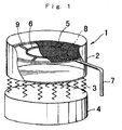
- the vibration screen classifier(1) equipped with an ultrasonic wave generator (transducer) (8) and is connected with a supporting base (4) by springs (3).
- the vibration screen classifier (1) comprises a cylindrical housing (2) having a ring-wise inner frame (9) engaging spokes to support a resonator ring (6) which is fixed to a metal mesh (5) and to the ultrasonic wave generator (8) which is being connected with a cable (7) to supply high frequency electric power.
- This vibration screen classifier (1) equipped with an ultrasonic wave generator (8) is driven by supplying a high frequency electric power, through cable (7), to the ultrasonic wave generator (8).
- the supplied high frequency electric power is, in the ultrasonic wave generator (8), converted to ultrasonic wave.
- the ultrasonic wave generated by generator (8) vibrates resonator ring (6) fixed to the ultrasonic wave generator (8) and to the ring-wise frame (9) on which the ultrasonic wave generator (8) is fixed, thereby the metal mesh (5) is vibrated in perpendicular direction to the surface of the screen mesh (5).
- the carrier according to the present invention can be obtained by classifying pulverized particles of magnetic material, or in case of core materials such as ferrite or magnetite, they may be preliminarily formed as first particles before sintering, then classified, and sintered, and classified, if desired.
- the carrier may be prepared by providing at first a resinous layer onto the core material, and then classifying the resinous layer-provided particles. In this case it is favorable that the classifications in each step of the resinous layer-provided particles are conducted using above described vibration screen classifier equipped with an ultrasonic wave generator.
- the core material used for constituting a carrier of the present invention includes various kind of known magnetic materials which have a magnetic moment, at 1 kOe of magnetic field are being imposed, of the carrier a level more than or equal to 70 emu / g, favorably more than or equal to 76 emu / g.
- the magnetic moment smaller than above degree is unfavorable, because the carrier is apt to easily deposit.
- B-H Tracer BHU-60 by Riken Denshi Co., Ltd.
- 1 gram of carrier core particles are plugged in a cylindrical cell, which is being set on the apparatus.
- applied magnetic field is gradually increased until it reaches to 3000 Oe, then it is gradually decreased to zero Oe, after that, reverse polarity of magnetic field is applied and it gradually increased until it reaches to 3000 Oe, then it is decreased to zero Oe, next, the same polarity as that of initially applied magnetic field is again applied, thereby a B-H.curve(B means magnetic flux dencity and H is magnetic susceptibility) is drawn in a graph, and from the drawing, magnetic moment of the carrier core at 1000 Oe of magnetic field is calculated.
- the core particle material used in the present invention which has a magnetic moment more than or equal to 70 emu/g at 1000 Oe of magnetic field includes for examples ferromagnetic substance such as iron, cobalt, magnetite, hematite, Li type of ferrite, Mn-Zn type of ferrite, Cu-Zn type of ferrite, Ni-Zn type of ferrite, Ba type of ferrite, Mn type of ferrite, and the like.
- favorable core particle material used in the present invention which has a magnetic moment more than or equal to 76 emu/g at 1000 Oe of magnetic field is instanced as iron, magnetite, Mn-Mg-Sr type of ferrite, Mn type of ferrite, and the like.
- Carrier of small bulk density is in general porous or has a high surface area concavo-convex. Smaller bulk density of the carrier is more disadvantageous for preventing the carrier deposition because even if the carrier has large amount of magnetic moment( emu/g) at 1000 Oe of magnetic field, substantial value of magnetic moment per particle is reduced. And plenty of concavo-convex causes a different thickness of resin coating by location, therefore unevenness of electric charge and electric resistance by location is likely to occur, effecting durability and carrier deposition for long period of running time.
- Specific resistance(log R • cm) of the carrier in the present invention is 12.0 or more, favorably 13.0 or more.
- the specific resistance less than above described degree is unfavorable, because in the case where the developing gap (the nearest distance between photosensitive member and development sleeve) becomes narrower, di-polarized electric charge is apt to be induced in the carrier, hence is apt to occur the carrier deposition.
- a tendency of the deterioration is shown in case of large linear velocity of photosensitive member and of large linear velocity of development sleeve are conducted, and when a biased AC voltage is applied the tendency becomes more significant.
- carrier for toner used in color developing is in general a carrier having low electric resistance. It has been now understood that the carrier of the present invention having above described degree of specific resistance, under the circumstance used in accompanied with a toner having a relevant amount of electric charge, yields an enough optical density of images.
- the specific resistance of the carrier in the present invention can be measured by a method described below.
- carrier (13) was filled in a cell which is made of fluoride resin and therein has electrodes (12a)(12b) of 2 mm distance and 2 ⁇ 4 cm of surface area, then DC electric voltage of 100 V was applied between the electrodes to determine a DC electric resistance which is shown on High Resistance Meter 4329A(4329A + LJK, 5HVLVWDQFH OHWHU manufactured by Yokogawa Hewlett-Packard Co. Ltd.) and to calculate the specific resistance(log R • cm) of the carrier.
- Adjustment of the specific resistance(log R • cm) of the carrier is able to execute by controlling of electric resistance and layer thickness of the resin to be coated upon carrier-core material. And it is possible to adjust the specific resistance of the carrier by adding a conductive finely divided powder into the coating resin.
- metal or metal oxide powders such as ZnO powder and A1 powder, SnO 2 prepared by various methods or doped by various elements, borides such as TiB 2 , ZnB 2 , MoB 2 , silicon carbide, conductive polymers such as poly(acethylene), poly(parapenylene), poly(parapenylene-sulfide) poly pyrrole, electro-conductive polyethylene, carbon blacks such as furnace black, acetylene black, channel black, are instanced.
- metal or metal oxide powders such as ZnO powder and A1 powder, SnO 2 prepared by various methods or doped by various elements, borides such as TiB 2 , ZnB 2 , MoB 2 , silicon carbide, conductive polymers such as poly(acethylene), poly(parapenylene), poly(parapenylene-sulfide) poly pyrrole, electro-conductive polyethylene, carbon blacks such as furnace black, acetylene black, channel black, are instanced.
- Those conductive finely divided powders may uniformly be dispersed by following manner; namely, by adding the conductive finely divided powder into a solvent used for coating or a resinous solution for coating, and admixing the solvent or solution by using dispersing apparatus or stirrer equipped with paddles rotable with high revolution speed.
- the carrier of the present invention is prepared by providing a resinous layer onto the surface of the particles of core material.
- resin materials for forming the resinous layer a silicon resin including the repeating units of formulas represented below is favorably used in the present invention; (where, R 1 indicates hydrogen atom, halogen atom, hydroxy group, methoxy group, lower alkyl group comprising 1 to 4 of carbon atoms, or aryl group such as phenyl group and tryl group, R 2 indicates alkylene group comprising 1 to 4 of carbon atoms, or arylene group such as phenylene group and trylene group).
- Straight silicone resins may be used in the present invention.
- these resins are, for instance, KR271, KR272, KR282, KR252, KR255 and KR152 (all made by Shin-Etsu Chemical Co. Ltd.), and SR2400, SR2406 (made by Dow Corning Toray Co., Ltd.).
- Modified silicone resins are also may be used in the present invention. Those are exemplified as epoxy resin-modified silicone, acrylic resin-modified silicone, phenollic resin-modified silicone, urethane-modified silicone, polyester resin-modified silicone, and alkyd resin-modified silicone resins.
- ES-1001N as the epoxy-modified
- KR-5208 as the acrylic-modified
- KR-5203 as the polyester-modified
- KR206 as the alkyd modified
- KR-305 as the urethane-modified
- SR-2115 as the epoxy-modified
- SR-2110 as the alkyd-modified (made by Dow Corning Toray Co., Ltd.).
- silicone resin used in the present invention may contain a relevant amount (0.001 to 30 % by weight) of amino-silane coupling agent comprising (this is why above description says 'essentially consisting of'), for example, as follows.
- the following resins may be employed as a coating material for coating the carrier core particles alone or in combination with silicone resin; styrene type resins including polystyrene, poly(chlorostyrene), poly- ⁇ -methylstyrene, styrene-chlorostyrene copolymer, styrene-propylene copolymer, styrene-butadiene copolymer, styrene-vinyl chloride copolymer, styrene-vinyl acetic acid copolymer, styrene-maleic acid copolymer, styrene-acrylic acid ester copolymer (such as styrene-methyl acrylate copolymer, styrene-ethyl acrylate copolymer, styrene-butyl acrylate copolymer, styrene-octyrene, polyst
- various known methods are applicable such as spray drying method, dipping method, powder coating method and the like, in particular, fluid bed type of coating apparatus is effective for obtaining uniform coating film in the present invention.
- the thickness of the resinous film provided onto the carrier core particles is as a rule in the range from 0.02 to 1.0 ⁇ m, favorably from 0.03 to 0.8 ⁇ m. This thickness of the resinous film is extremely thin, therefore size distributions of both the coated carrier core particles and source carrier core particles are substantially same.
- the developer of the present invention essentially consists of above mentioned carrier and toner.
- Toner used in the present invention is a mixture of coloring agent, finely divided particles, charge-controlling agent, repellant (in other words, releasing agent) and the like which are contained in the binder resins, mainly thermoplastic resins, in a conventional toner, and various known toners may be employed as the toner.
- the toners may have irregular form or spherical form and are prepared by various methods such as polymerization, pulverization, milling. They may be magnetic toners and non-magnetic toners.
- the binder resin of the toner includes those as below which may be employed alone or in combination.
- styrene type of binder resins include for examples homopolymer of stylene and its derivatives(such as polystyrene, polyvinyltoluene), copolymer (such as styrene-p-chlorostyrene copolymer, styrene-propylene copolymer, styrene-vinyltoluene copolymer, styrene-methyl acrylate copolymer, styrene-ethyl acrylate copolymer, styrene- butyl acrylate copolymer, styrene-methyl methacrylate copolymer, styrene-ethyl methacrylate copolymer, styrene- butyl methacrylate copolymer, styrene-methyl- ⁇ -chlormethacrylate copolymer, styrene-acrylonitrile cop
- acrylic resin includes for examples poly methyl methacrylate, poly butyl methacrylate.
- Others include, for example, polyvinyl chloride, polyvinyl acetate, polyethylene, polypropylene, polyester, polyurethane, epoxy resin, polyvinyl butyral, polyacrylic acid resin, rosins, modified rosin, terpenic resin, phenolic resin, resin of aliphatic or cycloaliphatic hydrocarbon type, aromatic petroleum resin, chlorinated paraffin, paraffin wax.
- the polyester resin can, in comparison with styrene type resins and acrylic resins, decrease the melt viscosity, while mainting storage stability.
- This kind of polyester resin is obtained by for example poly-condensation reaction of alcohol and carboxylic acid.
- the alcohol includes diols (such as poly(ethylene glycol), diethylene glycol, triethylene glycol, 1,2-propylene glycol, 1,3-propyleneglycol, 1,4-propylene glycol, neo-pentyl glycol, 1,4-butene diol; 1,4-bis-hydroxy-methyl cyclohexane, bisphenol A, hydrogenated bisphenol A, etherified bisphenols such as polyoxyethylene group-introduced bisphenol A and polyoxypropylene group-introduced bisphenol A, divalent alcoholic monomers which are derived from above each diols and are being substituted by saturated or unsaturated hydrocarbon group(s) having 3 to 22 carbon atoms, other divalent alcohols), triols (such as 1,2,4-butanetriol, 1,2,5-pentanetriol, glycerol, 2-methyl propanetriol, 2-methyl-1,2,4-butanetriol, trimethylol ethane, trimethlolpropane,
- the carboxylic acid employed for obtaining the polyester resin includes monocarboxylic acid (such as palmitic acid, stearic acid, oleic acid), dicarboxylic acid monomer(such as maleic acid, fumalic acid, mesaconic acid, citraconic acid, terephthalic acid, cyclohexane-dicarboxylic acid, succinic acid, adipic acid, sebatic acid, malonic acid, organic dibasic carboxylic acid which is derived from above each dicarboxylic acid and is being substituted by saturated or unsaturated hydrocarbon group(s) having 3 to 22 carbon atoms, anhydrides thereof, dimer derived from lower alkylester and linoleic acid), tribasic acid (such as 1,2,4-benzenetricarboxylic acid, 1,2,5-benzene tricarboxylic acid, 2,5,7-naphthalenetricarboxylic acid, 1,2,4-naphthalene tricarboxylic acid, 1,
- resin of epoxy type used in the present invention includes polycondensation products between bisphenol A and epochlohydrin, a part of which are commercially available as Epomick R362, R364, R365, R366, R367 and R369 (made by Mitsui Petrochemical Co. Ltd.), EpoToto YD-01, YD-012, YD-014, YD-904, YD-017 (made by Toto Chemical Co.), EPOCOAT 1002, 1004, 1007 (made by Shell Kagaku K. K.).
- Suitable materials as the coloring agent in the present invention include but are not limited to carbon black, lamp black, iron black, ultramarine, nigrosine, aniline black, phthalocyanine blue, Hansa yellow G, Rhodamine 6G lake, chalco-oil blue, chrome yellow, quinacridone, benzidine yellow, rose bengale, triarylmethane dyes, monoazo or diazo pigments and other known dyes and pigments.
- the toner may be used as a magnetic toner by incorporating a magnetic material powder therein.
- the magnetic material may be a ferromagnetic substance such as metallic iron and cobalt, powders of magnetite, hematite, Li type ferrite, Mn-Zn ferrite, Cu-Zn ferrite, Ni-Zn ferrite, Ba type ferrite and other magnetic materials.
- the toner composition of the present invention may also includes such additional materials as charge (or triboelectric charge ) controlling agents which are exemplified as metallic complexes such as mono-azo dyes, nitrohumic acid and salts thereof, amino compounds of Co, Cr, of Fe metal complexes with salicylic acid, naphthoic acid or dicarboxylic acid, quarternary ammonium compounds and organic dye materials.
- charge (or triboelectric charge ) controlling agents which are exemplified as metallic complexes such as mono-azo dyes, nitrohumic acid and salts thereof, amino compounds of Co, Cr, of Fe metal complexes with salicylic acid, naphthoic acid or dicarboxylic acid, quarternary ammonium compounds and organic dye materials.
- the toner composition of the present invention may also includes repellant, when necessary.
- repellant include but not limited to low molecular wieght polypropylene, low molecular weight polyethylene, carnauba wax, micro-crystalline wax, jojoba wax, rice wax and montan wax, and these waxes are used alone or in combination.
- the toner also may contain additives if desired. It is required for excellent quality of image to provide to the toner with a sufficient fluidity.
- a fluidity improving agent such as finely divided powders of metallic oxides which are having been hydrophobic treated or fine powder of lubricant to the toner is effective, and additives such as metallic oxide, finely divided powders of organic resin and metallic soaps may be employable.
- Illustrative examples thereof are a lubricant such as poly(tetrafluoro-ethylene) resin and zinc stearate, an abrasive such as cerium oxide or silicon carbide, a fluidity improving agent consisting of inorganic oxides such as SiO 2 and TiO 2 powders which are having been hydrophobic treated, a material known as anti-caking agent such as colloidal silica, aluminum oxide, and hydrophobic treated materials therefrom, and in particular hydrophobic silica is favorable for improving the fluidity of the toner.
- a lubricant such as poly(tetrafluoro-ethylene) resin and zinc stearate
- an abrasive such as cerium oxide or silicon carbide
- a fluidity improving agent consisting of inorganic oxides such as SiO 2 and TiO 2 powders which are having been hydrophobic treated
- a material known as anti-caking agent such as colloidal silica, aluminum oxide, and hydrophobic treated materials therefrom, and in particular hydrophobic si
- the toner used in the present invention has a weight-average particle-diameter (Dt) ranging from 9.0 to 4.0 ⁇ m, favorably from 7.5 to 4.5 ⁇ m.
- a ratio of the toner for carrier ranges from 2 to 25 weight parts, favorably from 4 to 15 weight parts of the toner per 100 weight parts of the carrier.
- coverage ratio by the toner for the carrier is 10 to 80 %, favorably 20 to 60 %.
- the toner charge per mass is less than 35 ⁇ c/g, favorably less than 25 ⁇ c/g.
- Coverage ratio (%) (Wt/Wc) ⁇ ( ⁇ c/ ⁇ t) ⁇ (Dc/Dt) ⁇ (1/4) ⁇ 100
- the Wt is toner weight(g)
- the Wc is carrier weight(g)
- the ⁇ c is true density of the carrier (g/cm 3 )
- the ⁇ t is true density of the toner(g/cm 3 )
- the Dc is weight average particle diameter of the carrier( ⁇ m)
- the Dt is weight average particle diameter of the toner( ⁇ m).
- Weight average particle diameters (Dw) of the carrier which is related to both carrier core and toner in the present invention, are values calculated from the basis obtained by measuring the particle size-distributions (showing the frequencies of particle number by particle diameter-division).
- the D is a representative particle size( ⁇ m) by each cannel having own size figure
- the n is total number of the particles detected in the each channel.
- the channel mentioned above is an unit for dividing the abscissa axis indicating particle size in the graph showing whole particle size-distribution, and each channel is 2 ⁇ m wide in case of the present invention.
- the representative particle size by each channel was designated as the smallest size in each channel in case of the present invention.
- particle diameters in the present invention were measured using a Micro-Track particle size analyzer (model HRA 9320-X 100 made by Honewell Co. Ltd), with following measuring conditions.
- the container for electrophotographic developer of the present invention is a developer-container containing the developer of the present invention therein.
- Various kinds of known containers may be used as the container.
- the image-forming apparatus of the present invention is an apparatus using, as developer-container, a container of the present invention.
- Various kinds of known image-forming apparatuses may be used as the apparatus.
- the image-forming method of the present invention is a method using, as developer, a developer of the present invention.
- Various kinds of known image-forming apparatuses may be used as the apparatus.
- a high quality of image having high optical density in the image with devoid of or scarce smear in back ground area can be produced by applying, as a biased electric-power to be added from external source during developing, a DC voltage overlapped by AC voltage.
- a DC voltage overlapped by AC voltage makes in general substantially large electric-potentials in both development point and background area, in comparison with the case of only DC voltage is applied. Therefore carrier depositions were apt to occur in conventional arts, however the carrier of the present invention makes possible to be compatible achievements of high optical density of image and avoidance of carrier deposition.
- the carrier of the invention having small diameter is used, if a small diameter carrier having a defined narrow particle-distribution noted as above is used, then a high quality image of excellent dot-reproducibility with very scarce or eliminated smear in back ground area and very scarce carrier deposition.
- Polyester resin 100 parts Magenta dye of quinacridone type 3.5 parts Fluorine-containing quaternary ammonium salt 4 parts
- Toner I To 100 parts of this mother toner was added by 0.8 parts of hydrophobic silica fine particles(R 972 ; made by Aerosil Japan Co. Ltd.) to obtain Toner I.
- Toner II having 5.8 ⁇ m of weight average diameter, 1.20 g/ cm 3 of true specific gravity was prepared from steps of preparing a mother toner by similar method as that of described Preparation of Toner 1, then adding 1.0 part of the hydrophobic silica particles (R 972; made by Aerosil Japan Co. Ltd.).
- Silicon resin (SR2411 made by Toray Dow-corning Ltd.) was diluted to a silicon resin solution (containing 5 % of solid).
- This solution was coated onto 5 kg of Carrier Core (i) having characteristics shown in Table I below (Mn-Mg-Sr type ferrite having 77 emu / g of magnetic moment at 1 kOe ) by using a fluidized bed-type of coating apparatus at rate of approximately 40 g / min., in an atmosphere at 100 °C, and the coating step was followed by heating for two hours at 240 °C, thus Carrier A having 5.0g/cm 3 of true specific gravity and 0.53 ⁇ m of coated layer thickness was obtained. Control of the thickness of the coated layer was conducted by adjusting the introduced amount of the coating liquid.
- Comparative Carrier B having 0.51 ⁇ m of coated layer and 5.0 g/ cm 3 of true specific gravity.
- Comparative Carrier C having 0.52 ⁇ m of coated layer and 5.0 g/ cm 3 of true specific gravity.
- Comparative Carrier D having 0.53 ⁇ m of coated layer and 5.0 g/cm 3 of true specific gravity.
- Comparative Carrier E having 0.51 ⁇ m of coated layer and 5.0 g/ cm 3 of true specific gravity.
- Carrier Core (vi) shown Table I, to obtain Carrier F having 0.51 ⁇ m of coated layer and 5.0 g/ cm 3 of true specific gravity.
- Carrier Core (vii) shown in Table I Similar method as that of described in Preparation of Carrier 1 was repeated with exception of using Carrier Core (vii) shown in Table I, to obtain Carrier G having 0.50 ⁇ m of coated layer and 5.0 g/cm 3 of true specific gravity.
- Carrier Core (viii) shown in Table I Similar method as that of described in Preparation of Carrier 1 was repeated with exception of using Carrier Core (viii) shown in Table I, to obtain Carrier H having 0.53 ⁇ m of coated layer and 5.0 g/ cm 3 of true specific gravity.
- Silicon resin (SR2411 made by Toray Dow-corning Ltd.) was diluted to a silicon resin solution(containing 5 % of solid). To the solution was added an amino silane coupling agent having a structure shown by H 2 N-(CH 2 ) 3 -Si-(OC 2 H 5 ) 3 at the ratio of 3 weight percent for the solid resin in the solution.
- Silicon resin (SR2411 made by Toray Dow-corning Ltd.) was diluted to a silicon resin solution(containing 5 % of solid).
- a carbon black registered trademark of Ketjen Black EC-DJ600 made by Lion Akzo Co. Ltd.
- an amino silane coupling agent having a structure shown by H 2 N-(CH 2 ) 3 -Si-(OC 2 H 5 ) 3 of 5 weight % for the solid resin weight were added into the solution, which was then dispersed for 60 minutes by a ball mill.
- Carrier Core Material (i) shown in Table I of 5 Kg was vibrated to classify using a vibration screen classifier equipped with an ultrasonic wave generator, to obtain Carrier Core (xi) shown in Table I.
- the vibration screen classifier is a classifier shown in Fig. 1, which is a sieving apparatus equipped with an ultrasonic wave generator(transducer) (8) generating ultrasonic waves having frequency of 36 kHz as a vibrator which is provided on a resonator ring (6) contacted with a metal screen (5) having 70 cm diameter and 635 mesh openings which is supported by a frame (9).
- the metal screen (5) is provided in a cylindrical container (2) which is supported by a base member (4) through springs (3).
- a vibrating motor (not shown in the Figure 1) which generates a high frequency electric current, and the generated electric current is, via cable (7), transferred to the ultrasonic wave generator (8) fixed in the resonator ring (6), thereby ultrasonic waves are generated.
- the ultrasonic waves By the ultrasonic waves, the resonator ring (6) is vibrated, thereby the metal mesh (5) is vibrated in perpendicular direction to the surface of the screen mesh (5).
- classified Carrier Core Material was recovered as Carrier Core XI from the upside of the screen mesh (5). There was no clogging of mesh (5).
- Coated Carrier O was obtained by similar method as that of described in Preparation of Carrier 1.
- Comparative Carrier D prepared in Preparation of Carrier 4 from Carrier Core (iv) was classified (removal of finer particles) using the vibration screen classifier used in above Preparation of Carrier 15, to obtain a Carrier D' of the present invention having diametric characteristics shown in Table I. was obtained.
- Carrier Core (iv) for Carrier D was a core material containing 8.5 weight % of small size less than 22 ⁇ m, in Carrier D' as a classified resultant, the content ratio 8.5 weight % of small size less than 22 ⁇ m was decreased to 0.5 weight %. There was no clogging of mesh (5).
- Imagio Color 4000 registered trademark of a copy machine having digital color image printing function manufactured by Ricoh Co. Ltd.
- Linear speed of photosensitive member 200 mm / sec.
- Ratio of linear speeds (of developing sleeve / of photosensitive member) 1.50
- Vd Charged electric potential
- Evaluations of the images reproduced were conducted on transferring paper sheets, while evaluations of carrier depositions were conducted by observation of the states on photosensitive member after developed and before transferring.
- Toner I of 10.1 parts was added to 100 parts of Carrier A, and they were agitated using a ball mill for 20 minutes, to yield 9.2weight % of developer. Covered ration to the Carrier A by Toner I was 50%, the toner charge per mass of Toner I was - 38 ⁇ c / g.
- Image density was 1.57, smear degree was Grade 8, small diameter of dots with variance of dot diameter as 0.17 were produced.
- Toner I of 9.2 parts was added to 100 parts of Carrier B, and they were agitated using a ball mill for 20 minutes, to yield 8.4weight % of developer. Covered ration to the Carrier B by Toner I was 50%, the toner charge per mass of Toner I was - 37 ⁇ c / g.
- Example 1 Evaluation of image quality was conducted in similar manner as that of Example 1 using Imagio Color 4000 revealed an identical carrier deposition as Example 1, however variance of dot diameter as 0.24 was larger than that of Example 1. Smear test after 50 K run revealed an increased smear than that of Example 1.
- the present invention can provide an excellent carrier and a developer giving high optical density of image with no smearing of background area, and showing good reproducibility in developing of small dots in image. Further, the carrier of the present invention has an excellent character that it is hard to result a so-called carrier deposition. Moreover, the present invention provides high quality and high reliability by combination of the carrier having specified electric and magnetic characteristics, and toner having a defined small diameter.
Landscapes
- Physics & Mathematics (AREA)
- General Physics & Mathematics (AREA)
- Chemical & Material Sciences (AREA)
- Crystallography & Structural Chemistry (AREA)
- Developing Agents For Electrophotography (AREA)
- Combined Means For Separation Of Solids (AREA)
Abstract
Description
- The present invention relates to a carrier for an electrophotographic developer, a developer using the carrier, a container for the developer, an image forming apparatus using the developer, an image forming method using the same and a preparation method of the carrier.
- There are proposed two developing methods in electrophotography; a so-called one-component developing method using one-component developer comprising merely a toner as a main ingredient, and a two-component developing method using a two-component developer comprising a mixture of a carrier made from materials such as glass beads, magnetic carrier, or those coated by resinous or other coatings, and a toner.
- The two-component developing method is advantageous in comparison with the one-component developing method, because it uses carrier which has a large surface area causing good triboelectric-charge for toner, thereby the charge of the toner is made stable, holding high quality in images for a long period of developing time. The two-component developing method also shows a high ability in the supply of the toner to the developing area, and therefore often has been employed particularly in high-speed apparatuses.
- In a digital electrophotographic system comprising the steps of forming latent electrostatic images on a photosensitive member by laser beam-irradiation and the like and then developing the latent images, the two-component developing method having the above characteristics is also being widely used.
- Recently, size reduction and condensed distribution of dot units for latent image (pixel units) have been designed to satisfy the requirements for improving the resolution degree, reproducibility of highlight image and faithful color-imaging. In, particular, important concern in the field is the achievement of a developing system which enables a faithful development of those latent images (dots composing each image). Therefore, many proposals were made from both points of processing means and developer (toner and carrier). As the processing means, a restriction of the development gap and a slenderization of the layers composing photosensitive member are effective, however there still remain problems with regard to the processing means that the processing cost is increased as a result of such improvements, and sufficient reliability is not yet achieved.
- On the other hand, with regard to the developer, the dot reproducibility is considerably improved by use of a small size toner. However, problems occur with a developer including small size toners, such as staining (or smear) in the background area is generated, optical image density decreases, etc. And, in case of toner having a small size which is used for full-color image, resins having a low softening-temperature are generally used which, in comparison with black toner, increase the spent amount on the surface of carrier, and degrade the quality of developer by lapse of time and show a tendency apt to toner-scattering and to stain the background area.
- Various proposals for use of small size carriers are also proposed. For example, Japanese Patent No. 2832013 discloses a developing method for reversal development of a latent electrostatic image formed on a latent image-bearing member having an organic photo-conductive layer, using magnetic brush of two-component developer which is held on a developer-bearing member and contains a toner capable of being charged in the same polarity as that of the latent image and a carrier, with imposing a biased electric field having an alternating current component and a direct current component, wherein the carrier is a carrier including ferrite core-material particles, the core-material particles are being coated with an electric insulating-resin and having a weight-average diameter ranging from 30 to 65 µm after coated with the resin, and the core-material particles have, at their surfaces, small pores of 1500 Å to 30000 Å in average size.
- Japanese Patent No. 3029180 discloses a carrier for an electrophotographic developer using carrier particles, wherein the carrier particles have a size ranging from 15 to 45 µm in 50%-average diameter (D50) (D50 represents a particles amount summed up every ingredient divisions by size till becomes to 50%), the content of smaller carrier particles less than 22µm in size ranges from 1 to 20%, the content of small carrier particles less than 16µm in size is not higher than 3%, the content of large carrier particles more than or equal to 62µm in size ranges from 2 to 15%, the content of larger carrier particles more than 88µm in size is not higher than 2%, and the carrier satisfies a ratio( S1/S2) of surface area (S1) measured by air-permeation method in comparison with surface area(S2), a range represented by;
- Further, Japanese Unexamined Patent Publication of Tokkai Hei 10-198077 discloses a carrier for developer used for developing electrostatic latent image, wherein a 50%-average diameter (D50) in volumetric average diameter of the carrier ranges from 30 to 80µm, a ratio (D50 / D10) of the D50 for a 10%-average diameter (D10) in volumetric average diameter of the carrier is 1.8 or less, a ratio (D90 / D50) of a 90%-average diameter (D90) in volumetric average diameter of the carrier for the 50%-average diameter (D50) in volumetric average diameter of the carrier is 1.8 or less, the magnetic moment (at 1 kilo Oe of magnetic field) of the carrier ranges from 52 to 65 emu / g.
- By the use of this kind of carriers having small diameter gives following benefits;
- (1) Surface area per unit volume is large, therefore they can give satisfactory triboelectric-charge for each toner, and scarcely yield toners which have a low level of electric-charge and reverse polarity-charge. Accordingly, there is little scattering of toner particles at the periphery of dot for image-forming and smear (blurring) in the background area, thus dot reproducibility is excellent;
- (2) Due to the nature of large surface area per unit volume and scarce to generate the smear in background area, a low level of average electric-charge in toner is allowable to use, notwithstanding, a high optical density of image is obtained, thus carrier of small diameter is capable to compensate the shortcomings which are caused by use of small size of toner, hence is effective for driving out the advantages of small size of toner;
- (3) As small diameter of carrier forms a dense magnetic brush and the head of the formed magnetic brush has an excellent fluidity. Accordingly, the trace drawn by dragging of the head of the magnetic brush on image is hardly imprinted.
-
- However, carriers of small diameter in the prior art have a important problem that they are apt to deposit on surfaces contacted with the developer, thus bringing flaws on photosensitive member or fixing roller. Therefore, it was difficult to use them in practice.
- With regard to carriers of small diameter, the inventors have investigated diameters of carriers deposited on the surfaces of the photosensitive member and found out that, out of used original carrier having a size-distribution, the smaller size carrier particles show a tendency to preferentially deposit on the surface of photosensitive member, and the deposited ratio of smaller size particles of less than 22 µm diameter was overwhelmingly much in all deposited particles.
- Accordingly, a first object of the invention is to provide a carrier for an electrophotographic developer and a developer using the same which are able to produce high quality image-reproductions having an excellent dot-reproducibility, an excellent highlight-reproducibility, a high optical image density, and showing scarce or no smear in background area.
- A further object of the present invention is to provide a container for the developer.
- A still further object of the present invention is to provide an image-forming apparatus that has loaded the container for the developer.
- A further object of the present invention is to provide a preparation method for the carrier.
- Above and other objects are achieved by the present invention comprising;
- (1) A carrier for electrophotographic developer comprising carrier particles, each carrier
particle comprising a magnetic core particle and a resin layer formed on the surface of
said magnetic core particle, and said carrier having a magnetic moment of 76 emu/g or
more at 1 kOe, and said carrier particles having a weight-average particle diameter (Dw)
in a range of 25 to 45 micrometer, and said carrier particles comprising:
- (1) carrier component particles having a diameter of less than 44 micrometer in an amount of 75 wt.% or more,
- (2) carrier component particles having a diameter of 62 micrometer or more in an amount of less than 1 wt.%, and
- (3) carrier component particles having a diameter of less than 22 micrometer in an amount of 7.0 wt.% or less, based on the total amount of said carrier particles;
- (2) A carrier for electrophotographic developer according to above paragraph (1), characterized by said carrier component particles having a diameter of less than 22 micrometer is in an amount of 3.0 wt.% or less;
- (3) A carrier for electrophotographic developer according to above paragraph (1), characterized by said carrier component particles having a diameter of less than 22 micrometer is in an amount of 1.0 wt.% or less;
- (4) A carrier for electrophotographic developer according to any one of above paragraph (1) to (3), characterized by the bulk density of the carrier being of 2.2 g / cm3 or more;
- (5) A carrier for electrophotographic developer according to any one of above paragraph (1) to (4), characterized by the specific electric-resistance denoted by (log R • cm) of the carrier has a value of 12.0 or more;
- (6) A carrier for electrophotographic developer according to any one of above paragraph (1) to (5), characterized by the magnetic core particle being a MnMgSr ferrite material;
- (7) A carrier for electrophotographic developer according to any one of above paragraph (1) to (5), characterized by the magnetic core particle being a Mn ferrite material;
- (8) A carrier for electrophotographic developer according to any one of above paragraph (1) to (5), characterized by the magnetic core particle being a magnetite material;
- (9) A carrier for electrophotographic developer according to any one of above paragraph (1) to (8), characterized by the resinous coating layer being a silicone resin coating layer;
- (10) A carrier for electrophotographic developer according to any one of above paragraph (1) to (9), characterized by the resin layer comprising a resin layer containing a reaction product with an amino silane type coupling agent.
-
- Further, above and other objects are also achieved by the present invention including;
- (11) An electrophotographic developer using a toner and a carrier comprising carrier
particles, each carrier particle comprising a magnetic core particle and a resin layer
formed on the surface of said magnetic core particle, and said carrier having a magnetic
moment of 76 emu/g or more at 1 kOe, and said carrier particles having a
weight-average particle diameter (Dw) in a range of 25 to 45 micrometer, and said
carrier particles comprising:
- (1) carrier component particles having a diameter of less than 44 micrometer in an amount of 75 wt.% or more,
- (2) carrier component particles having a diameter of 62 micrometer or more in an amount of less than 1 wt.%, and
- (3) carrier component particles having a diameter of less than 22 micrometer in an amount of 7.0 wt.% or less, based on the total amount of said carrier particles;
- (12) An electrophotographic developer using a toner and a carrier according to above paragraph (11), characterized in that the toner charge per mass is less than or equal to 35 µC /g at coverage ratio 50% on the surface of the carrier by the toner;
- (13) An electrophotographic developer using a toner and a carrier according to above paragraph (11) or (12), characterized in that the toner charge per mass at 50 % is less than or equal to 25 µC /g at coverage ratio 50% on the surface of the carrier by the toner;
- (14) An electrophotographic developer using a toner and a carrier according to any one of above paragraph (11) to (13), characterized in that the toner has a weight-average particle-diameter of less than or equal to 6.0µm.
-
- Furthermore, above and other objects are also achieved by the present invention including;
- (15) A container for electrophotographic developer using a toner and a apparatus loaded
with a carrier comprising carrier particles, each carrier particle comprising a magnetic
core particle and a resin layer formed on the surface of said magnetic core particle, and
said carrier having a magnetic moment of 76 emu/g or more at 1 kOe, and said carrier
particles having a weight-average particle diameter (Dw) in a range of 25 to 45
micrometer, and said carrier particles comprising;
- (1) carrier component particles having a diameter of less than 44 micrometer in an amount of 75 wt.% or more,
- (2) carrier component particles having a diameter of 62 micrometer or more in an amount of less than 1 wt.%, and
- (3) carrier component particles having a diameter of less than 22 micrometer in an amount of 7.0 wt.% or less, based on the total amount of said carrier particles.
-
- Still further, above and other objects are also achieved by the present invention including;
- (16) An image forming apparatus loaded with a container for electrophotographic
developer, characterized by the developer uses a toner and a carrier comprising carrier
particles, each carrier particle comprising a magnetic core particle and a resin layer
formed on the surface of said magnetic core particle, and said carrier having a magnetic
moment of 76 emu/g or more at 1 kOe, and said carrier particles having a
weight-average particle diameter (Dw) in a range of 25 to 45 micrometer, and said
carrier particles comprising:
- (1) carrier component particles having a diameter of less than 44 micrometer in an amount of 75 wt.% or more,
- (2) carrier component particles having a diameter of 62 micrometer or more in an amount of less than 1 wt.%, and
- (3) carrier component particles having a diameter of less than 22 micrometer in an amount of 7.0 wt.% or less, based on the total amount of said carrier particles;
-
- Still further, above and other objects are also achieved by the present invention including;
- (17) An image forming method using an electrophotographic developer, characterized
by the developer uses a toner and a carrier comprising carrier particles, each carrier
particle comprising a magnetic core particle and a resin layer formed on the surface of
said magnetic core particle, and said carrier having a magnetic moment of 76 emu/g or
more at 1 kOe, and said carrier particles having a weight-average particle diameter (Dw)
in a range of 25 to 45 micrometer, and said carrier particles comprising:
- (1) carrier component particles having a diameter of less than 44 micrometer in an amount of 75 wt.% or more,
- (2) carrier component particles having a diameter of 62 micrometer or more in an amount of less than 1 wt.%, and
- (3) carrier component particles having a diameter of less than 22 micrometer in an amount of 7.0 wt.% or less, based on the total amount of said carrier particles;
-
- Still further, above and other objects are also achieved by the present invention including;
- (18) A preparation method of a carrier for electrophotographic developer comprising
carrier particles, each carrier particle comprising a magnetic core particle and a resin
layer formed on the surface of said magnetic core particle, and said carrier having a
magnetic moment of 76 emu/g or more at 1 kOe, and said carrier particles having a
weight-average particle diameter (Dw) in a range of 25 to 45 micrometer, and said
carrier particles comprising:
- (1) carrier component particles having a diameter of less than 44 micrometer in an amount of 75 wt.% or more,
- (2) carrier component particles having a diameter of 62 micrometer or more in an amount of less than 1 wt.%, and
- (3) carrier component particles having a diameter of less than 22 micrometer in an amount of 7.0 wt.% or less, based on the total amount of said carrier particles; and comprising steps of (i) classifying a magnetic material of finely pulverized particles, thereby obtaining a core material of particles having a weight-average particle-diameter (Dw) of the carrier ranges from 25 to 45µm, the content of particles having a diameter of less than 44 µm is more than or equal to 75 % by weight, the content of particles having a diameter of more than or equal to 62µm is less than one percent by weight, the content of particles having a diameter of less than 22µm is less than or equal to 7.0 % by weight, the magnetic moment of the carrier at 1 kOe of magnetic field is more than or equal to 76 emu / g, (ii) providing a resinous film on the magnetic core material;
- (19) A preparation method of a carrier for electrophotographic developer comprising
carrier particles, each carrier particle comprising a magnetic core particle and a resin
layer formed on the surface of said magnetic core particle, and said carrier having a
magnetic moment of 76 emu/g or more at 1 kOe, and said carrier particles having a
weight-average particle diameter (Dw) in a range of 25 to 45 micrometer, and said
carrier particles comprising:
- (1) carrier component particles having a diameter of less than 44 micrometer in an amount of 75 wt.% or more,
- (2) carrier component particles having a diameter of 62 micrometer or more in an amount of less than 1 wt.%, and
- (3) carrier component particles having a diameter of less than 22 micrometer in an amount of 7.0 wt.% or less, based on the total amount of said carrier particles; and comprising steps of (i) providing a resinous film onto a magnetic core material of finely pulverized particles, (ii) classifying the magnetic core material of finely pulverized particles having resinous film thereon, thereby obtaining a core material of particles having a weight-average particle-diameter (Dw) of the carrier ranges from 25 to 45 µm, the content of particles having a diameter of less than 44 µm is more than or equal to 75 % by weight, the content of particles having a diameter of more than or equal to 62 µm is less than one percent by weight, the content of particles having a diameter of less than 22 µm is less than or equal to 7.0 % by weight, the magnetic moment of the carrier at 1 kOe is more than or equal to 76 emu/g;
- (20) A preparation method of the carrier according to above paragraph (18), characterized by a vibration sieve equipped with an ultrasonic wave-generator is used in the step of (i) classifying a magnetic material of finely pulverized particles;
- (21) A preparation method of the carrier according to above paragraph (19), characterized by a vibration sieve equipped with an ultrasonic wave-generator is used in the step of (ii) classifying the magnetic core material of finely pulverized particles having a resinous film thereon;
- (22) A preparation method of the carrier according to above paragraph (20) or (21), characterized by a vibration sieve, which is equipped with an ultrasonic wave-generator and a resonator ring to transfer ultrasonic waves generated by the ultrasonic wave-generator to the vibration sieve, is used in the step of classifying a magnetic material of finely pulverized particles.
-
- The carrier for electrophotographic developer (sometimes merely referred to as the carrier hereinafter) of the present invention consists of a core material of magnetic particles provided with a resinous layer.
- With regard to the carrier of the present invention, weight-average particle-diameter (Dw) thereof ranges from 25µm to 45µm, favorably from 30µm to 45µm. Larger weight-average particle-diameter (Dw) than above range is hard to deposit the carrier, however the condensation of toner content in the developer for the sake of obtaining a high optical density of image increases smear (stain) of background area abruptly, and causes a large variance of dot diameter in case of development of small dot for latent image.
- The carrier deposition in the present invention means a phenomenon of depositing carrier onto the electrostatic latent image area or background area. The stronger electric field at both areas shows more abundance deposition of carrier. However image area is as a rule decreased in the strength of electric field by developing with toner. Therefore, it is hard to deposit carrier in comparison with background area. As described above, carrier deposition causes flaws on photosensitive member or fixing roller and thus is unfavorable.
- In the carrier of the present invention, the content of particles having a diameter of less than or equal to 44µm is more than or equal to 70 % by weight, favorably more than or equal to 75 % by weight. And the content of particles having a diameter of less than or equal to 44µm is favorably less than or equal to 95 % by weight, more favorably less than or equal to 90 % by weight. Within the content ratio of less than or equal to 95 % by weight, one can obtaine a carrier having a desired size without excess expenditure.
- The content of particles having a diameter of more than 62µm is less than three percent by weight, favorably less than one percent. And the content of particles having a diameter of more than 62µm is more than 0.3 percent by weight. Within the content ratio of more than or equal to 0.3 % by weight, one can obtaine a carrier having a desired size without excess expenditure.
- The larger content of particles having diameter more than 62µm causes more noticeable scattering in dot sizes of latent image. It is thought that this tendency depends upon the fact that, in case of carrier particles having diameter more than 62µm, a small increase in size significantly influences the reduction of percentage by weight of carriers having a diameter ranging from 44 µm to 62µm. The content of particles having a diameter of less than 22µm is less than seven percent by weight, favorably less than 3 percent, more favorably less than 1 percent. The content of particles having a diameter of less than 22µm is less than 7 percent by weight, favorably less than 3 percent, more favorably less than 1 percent. And the content of particles having a diameter of less than 22µm is more than or equal to 0.1 percent by weight. Within the content ratio of more than or equal to 0.1 % by weight, one can obtaine a carrier having desired size without excess expenditure.
- In case of carrier having a small diameter(size), a majority of carriers deposited are those fine particles having a diameter of less than 22µm. We have evaluated carrier depositions with varied content ratios of smaller particles of less than 22µm diameter in small carrier particles of size ranging from 25µm to 45µm, and arrived at the conclusion that no serious problem is presented in the case of content of small particles of less than 22µm diameter is less than or equal to 7 percent, and carrier deposition is improved by the content less than or equal to 3 percent, and more improved by restricting the content to a level less than or equal to 1 percent.
- At the same time, it was found out that carrier deposition is also substantially evaded by controlling the magnetic moment of the carrier at 1 kOe, to a level more than or equal to 76 emu/g.
- The carrier of the present invention can prepared by pulverizing a magnetic material, classifying the finely pulverized particles so as to obtain a core material of particles having the defined average particle-diameter (Dw) and the defined distribution in average particle-diameters of the particles, then providing a resinous film on the classified magnetic core material.
- Above classification includes pneumatic classification, screen classification and the like. Vibration sieves have been used favorably, however a conventional vibration sieve has the inconvenience that mesh-straggle (clogging) occurs in case of classification for small size of particles, thus deterioriating operation efficiency.
- We have studied to develop a method capable of removal small size of particles with high efficient, and arrived to a result that small particles of less than 22µm diameter are removed efficiently and sharply by adding a vibration using ultrasonic waves to screen mesh in screen classification process.
- The ultrasonic wave-vibration for vibrating the screen mesh can be obtained by giving an electric power of high frequency to a converter (transducer) which uses a PZT vibrator and converts electric power to an ultrasonic wave generating vibration power. For making a vibration in screen mesh, ultrasonic wave vibration is transferred to a resonator member which is being fixed to the screen mesh, and the resonator member is resonated with the vibration of ultrasonic wave to make vibration for the screen mesh. The ultrasonic wave frequency for vibrating the screen mesh ranges from 20 to 50 kHz, 30 to 40 kHz is favorable. The form of the resonator member may be any one suitable to make vibration in the screen mesh, and generally is a ring form. Direction to make vibration of the screen mesh is favorably perpendicular to the surface of the screen mesh.
-
- FIG. 1 is a perspective view of an embodiment of a vibration screen classifier equipped with an ultrasonic wave vibrator and favorably used in the present invention.
- FIG. 2 is a perspective view of an electric resistance-measuring cell used for measuring the electric resistance of the carrier according to the invention.
-
- With regard to the classifier shown in Fig 1, the vibration screen classifier(1) equipped with an ultrasonic wave generator (transducer) (8) and is connected with a supporting base (4) by springs (3). The vibration screen classifier (1) comprises a cylindrical housing (2) having a ring-wise inner frame (9) engaging spokes to support a resonator ring (6) which is fixed to a metal mesh (5) and to the ultrasonic wave generator (8) which is being connected with a cable (7) to supply high frequency electric power.
- This vibration screen classifier (1) equipped with an ultrasonic wave generator (8) is driven by supplying a high frequency electric power, through cable (7), to the ultrasonic wave generator (8). The supplied high frequency electric power is, in the ultrasonic wave generator (8), converted to ultrasonic wave. The ultrasonic wave generated by generator (8) vibrates resonator ring (6) fixed to the ultrasonic wave generator (8) and to the ring-wise frame (9) on which the ultrasonic wave generator (8) is fixed, thereby the metal mesh (5) is vibrated in perpendicular direction to the surface of the screen mesh (5).
- This type of vibration screen classifier equipped with an ultrasonic wave generator is now commercially available, for example, as "ULTRASONIC" made by Koei Sangyo Co. Ltd.
- The carrier according to the present invention can be obtained by classifying pulverized particles of magnetic material, or in case of core materials such as ferrite or magnetite, they may be preliminarily formed as first particles before sintering, then classified, and sintered, and classified, if desired. Alternatively, the carrier may be prepared by providing at first a resinous layer onto the core material, and then classifying the resinous layer-provided particles. In this case it is favorable that the classifications in each step of the resinous layer-provided particles are conducted using above described vibration screen classifier equipped with an ultrasonic wave generator.
- The core material used for constituting a carrier of the present invention includes various kind of known magnetic materials which have a magnetic moment, at 1 kOe of magnetic field are being imposed, of the carrier a level more than or equal to 70 emu / g, favorably more than or equal to 76 emu / g. There is no upper limit of it in the present invention, however as a rule is 150 emu / g or the less. The magnetic moment smaller than above degree is unfavorable, because the carrier is apt to easily deposit.
- Above described magnetic moment can be measured as follow.
- With use of B-H Tracer(BHU-60 by Riken Denshi Co., Ltd.), 1 gram of carrier core particles are plugged in a cylindrical cell, which is being set on the apparatus. Thereto applied magnetic field is gradually increased until it reaches to 3000 Oe, then it is gradually decreased to zero Oe, after that, reverse polarity of magnetic field is applied and it gradually increased until it reaches to 3000 Oe, then it is decreased to zero Oe, next, the same polarity as that of initially applied magnetic field is again applied, thereby a B-H.curve(B means magnetic flux dencity and H is magnetic susceptibility) is drawn in a graph, and from the drawing, magnetic moment of the carrier core at 1000 Oe of magnetic field is calculated.
- The core particle material used in the present invention which has a magnetic moment more than or equal to 70 emu/g at 1000 Oe of magnetic field includes for examples ferromagnetic substance such as iron, cobalt, magnetite, hematite, Li type of ferrite, Mn-Zn type of ferrite, Cu-Zn type of ferrite, Ni-Zn type of ferrite, Ba type of ferrite, Mn type of ferrite, and the like. Ferrite is in general sintered substance shown by following Formula 2;
- As examples of favorable core particle material used in the present invention which has a magnetic moment more than or equal to 76 emu/g at 1000 Oe of magnetic field is instanced as iron, magnetite, Mn-Mg-Sr type of ferrite, Mn type of ferrite, and the like.
- Bulk density of the carrier more than or equal to 2.2g/cm3, favorably more than or equal to 2.3g/cm3 is advantageous for preventing the carrier deposition. Carrier of small bulk density is in general porous or has a high surface area concavo-convex. Smaller bulk density of the carrier is more disadvantageous for preventing the carrier deposition because even if the carrier has large amount of magnetic moment( emu/g) at 1000 Oe of magnetic field, substantial value of magnetic moment per particle is reduced. And plenty of concavo-convex causes a different thickness of resin coating by location, therefore unevenness of electric charge and electric resistance by location is likely to occur, effecting durability and carrier deposition for long period of running time.
- Specific resistance(log R • cm) of the carrier in the present invention is 12.0 or more, favorably 13.0 or more. The specific resistance less than above described degree is unfavorable, because in the case where the developing gap (the nearest distance between photosensitive member and development sleeve) becomes narrower, di-polarized electric charge is apt to be induced in the carrier, hence is apt to occur the carrier deposition. A tendency of the deterioration is shown in case of large linear velocity of photosensitive member and of large linear velocity of development sleeve are conducted, and when a biased AC voltage is applied the tendency becomes more significant. Usually, carrier for toner used in color developing is in general a carrier having low electric resistance. It has been now understood that the carrier of the present invention having above described degree of specific resistance, under the circumstance used in accompanied with a toner having a relevant amount of electric charge, yields an enough optical density of images.
- The specific resistance of the carrier in the present invention can be measured by a method described below.
- As shown Fig. 2, carrier (13) was filled in a cell which is made of fluoride resin and therein has electrodes (12a)(12b) of 2 mm distance and 2 × 4 cm of surface area, then DC electric voltage of 100 V was applied between the electrodes to determine a DC electric resistance which is shown on High Resistance Meter 4329A(4329A + LJK, 5HVLVWDQFH OHWHU manufactured by Yokogawa Hewlett-Packard Co. Ltd.) and to calculate the specific resistance(log R • cm) of the carrier.
- Adjustment of the specific resistance(log R • cm) of the carrier is able to execute by controlling of electric resistance and layer thickness of the resin to be coated upon carrier-core material. And it is possible to adjust the specific resistance of the carrier by adding a conductive finely divided powder into the coating resin. As the conductive finely divided powder, metal or metal oxide powders such as ZnO powder and A1 powder, SnO2 prepared by various methods or doped by various elements, borides such as TiB2, ZnB2, MoB2, silicon carbide, conductive polymers such as poly(acethylene), poly(parapenylene), poly(parapenylene-sulfide) poly pyrrole, electro-conductive polyethylene, carbon blacks such as furnace black, acetylene black, channel black, are instanced.
- Those conductive finely divided powders may uniformly be dispersed by following manner; namely, by adding the conductive finely divided powder into a solvent used for coating or a resinous solution for coating, and admixing the solvent or solution by using dispersing apparatus or stirrer equipped with paddles rotable with high revolution speed.
- The carrier of the present invention is prepared by providing a resinous layer onto the surface of the particles of core material. As resin materials for forming the resinous layer, a silicon resin including the repeating units of formulas represented below is favorably used in the present invention;(where, R1 indicates hydrogen atom, halogen atom, hydroxy group, methoxy group, lower alkyl group comprising 1 to 4 of carbon atoms, or aryl group such as phenyl group and tryl group, R2 indicates alkylene group comprising 1 to 4 of carbon atoms, or arylene group such as phenylene group and trylene group).

- Straight silicone resins may be used in the present invention. Examples of these resins are, for instance, KR271, KR272, KR282, KR252, KR255 and KR152 (all made by Shin-Etsu Chemical Co. Ltd.), and SR2400, SR2406 (made by Dow Corning Toray Co., Ltd.).
- Modified silicone resins are also may be used in the present invention. Those are exemplified as epoxy resin-modified silicone, acrylic resin-modified silicone, phenollic resin-modified silicone, urethane-modified silicone, polyester resin-modified silicone, and alkyd resin-modified silicone resins.
- Specific examples thereof are, for instance, ES-1001N as the epoxy-modified, KR-5208 as the acrylic-modified, KR-5203 as the polyester-modified, KR206 as the alkyd modified, KR-305 as the urethane-modified (all which are made by Shin-Etsu Chemical Co. Ltd.), SR-2115 as the epoxy-modified, SR-2110 as the alkyd-modified (made by Dow Corning Toray Co., Ltd.).
- Above mentioned silicone resin used in the present invention may contain a relevant amount (0.001 to 30 % by weight) of amino-silane coupling agent comprising (this is why above description says 'essentially consisting of'), for example, as follows.
H2N(CH2)3 • Si(OCH3)3 MW 179.3 H2N(CH2)3 • Si(OC2H5)3 MW 221.4 H2N • CH2 • CH2 • CH2 • Si(CH3)2 • (OC2H5) MW 161.3 H2N • CH2 • CH2 • CH2 • Si(CH3) • (OC2H5)2 MW 191.3 H2N • CH2 • CH2 • HN • CH2 • Si(OCH3)3 MW 194.3 H2N(CH2)2 • HN • (CH2)3 • Si(CH3) • (OCH3)2 MW 206.4 H2N(CH2)2 • HN • (CH2)3 • Si(OCH3)3 MW 224.4 (CH3)2 • N • (CH2)3 • Si(CH3) • (OC2H5)2 MW 219.4 (C4H9)2 • N • (CH2)3 • Si(OCH3)3 MW 291.6 - Furthermore, in the present invention, the following resins may be employed as a coating material for coating the carrier core particles alone or in combination with silicone resin; styrene type resins including polystyrene, poly(chlorostyrene), poly- α -methylstyrene, styrene-chlorostyrene copolymer, styrene-propylene copolymer, styrene-butadiene copolymer, styrene-vinyl chloride copolymer, styrene-vinyl acetic acid copolymer, styrene-maleic acid copolymer, styrene-acrylic acid ester copolymer (such as styrene-methyl acrylate copolymer, styrene-ethyl acrylate copolymer, styrene-butyl acrylate copolymer, styrene-octyl acrylate copolymer, styrene-phenyl acrylate copolymer), styrene-methacrylic acid ester copolymer (such as styrene-methyl methacrylate copolymer, styrene-ethyl methacrylate copolymer, styrene-butyl methacrylate copolymer, styrene-phenyl methacrylate copolymer), styrene-methyl-α -chloracrylate copolymer, styrene-acrylonitrile-acrylic acid ester copolymer; epoxy resin; polyester resin, polyethylene resin, polypropylene resin, ionomer resin, polyurethane resin, ketone resin, ethylene-ethyl acrylate copolymer, xylene resin, polyamide resin, phenolic resin, polycarbonate resin, melamine resin, fluorine-containing resin,and the like.
- With regard to the method of providing the resinous layer on the surface of the carrier core particles, various known methods are applicable such as spray drying method, dipping method, powder coating method and the like, in particular, fluid bed type of coating apparatus is effective for obtaining uniform coating film in the present invention.
- The thickness of the resinous film provided onto the carrier core particles is as a rule in the range from 0.02 to 1.0 µm, favorably from 0.03 to 0.8 µm. This thickness of the resinous film is extremely thin, therefore size distributions of both the coated carrier core particles and source carrier core particles are substantially same.
- The developer of the present invention essentially consists of above mentioned carrier and toner. Toner used in the present invention is a mixture of coloring agent, finely divided particles, charge-controlling agent, repellant (in other words, releasing agent) and the like which are contained in the binder resins, mainly thermoplastic resins, in a conventional toner, and various known toners may be employed as the toner. The toners may have irregular form or spherical form and are prepared by various methods such as polymerization, pulverization, milling. They may be magnetic toners and non-magnetic toners.
- The binder resin of the toner includes those as below which may be employed alone or in combination.
- As styrene type of binder resins include for examples homopolymer of stylene and its derivatives(such as polystyrene, polyvinyltoluene), copolymer (such as styrene-p-chlorostyrene copolymer, styrene-propylene copolymer, styrene-vinyltoluene copolymer, styrene-methyl acrylate copolymer, styrene-ethyl acrylate copolymer, styrene- butyl acrylate copolymer, styrene-methyl methacrylate copolymer, styrene-ethyl methacrylate copolymer, styrene- butyl methacrylate copolymer, styrene-methyl- α -chlormethacrylate copolymer, styrene-acrylonitrile copolymer, styrene-vinylmethylether copolymer, styrene-vinylmethylketone copolymer, styrene-butadiene copolymer, styrene-isoprene copolymer, styrene-maleic acid copolymer, styrene-maleic acid ester copolymer.
- As acrylic resin includes for examples poly methyl methacrylate, poly butyl methacrylate.
- Others include, for example, polyvinyl chloride, polyvinyl acetate, polyethylene, polypropylene, polyester, polyurethane, epoxy resin, polyvinyl butyral, polyacrylic acid resin, rosins, modified rosin, terpenic resin, phenolic resin, resin of aliphatic or cycloaliphatic hydrocarbon type, aromatic petroleum resin, chlorinated paraffin, paraffin wax.
- The polyester resin can, in comparison with styrene type resins and acrylic resins, decrease the melt viscosity, while mainting storage stability. This kind of polyester resin is obtained by for example poly-condensation reaction of alcohol and carboxylic acid.
- The alcohol includes diols (such as poly(ethylene glycol), diethylene glycol, triethylene glycol, 1,2-propylene glycol, 1,3-propyleneglycol, 1,4-propylene glycol, neo-pentyl glycol, 1,4-butene diol; 1,4-bis-hydroxy-methyl cyclohexane, bisphenol A, hydrogenated bisphenol A, etherified bisphenols such as polyoxyethylene group-introduced bisphenol A and polyoxypropylene group-introduced bisphenol A, divalent alcoholic monomers which are derived from above each diols and are being substituted by saturated or unsaturated hydrocarbon group(s) having 3 to 22 carbon atoms, other divalent alcohols), triols (such as 1,2,4-butanetriol, 1,2,5-pentanetriol, glycerol, 2-methyl propanetriol, 2-methyl-1,2,4-butanetriol, trimethylol ethane, trimethlolpropane, 1,3,5-trihydroxymethylbenzene), sorbitol, 1,2,3,6-hexane tetrol, 1,4-sorbitan, pentaerythritol, di-pentaerythritol, tri-pentaerythritol, saccharose.
- The carboxylic acid employed for obtaining the polyester resin includes monocarboxylic acid (such as palmitic acid, stearic acid, oleic acid), dicarboxylic acid monomer(such as maleic acid, fumalic acid, mesaconic acid, citraconic acid, terephthalic acid, cyclohexane-dicarboxylic acid, succinic acid, adipic acid, sebatic acid, malonic acid, organic dibasic carboxylic acid which is derived from above each dicarboxylic acid and is being substituted by saturated or unsaturated hydrocarbon group(s) having 3 to 22 carbon atoms, anhydrides thereof, dimer derived from lower alkylester and linoleic acid), tribasic acid (such as 1,2,4-benzenetricarboxylic acid, 1,2,5-benzene tricarboxylic acid, 2,5,7-naphthalenetricarboxylic acid, 1,2,4-naphthalene tricarboxylic acid, 1,2,4-butanetricarboxylic acid, 1,2,5-hexane tricarboxylic acid, 1,3-dicarboxyl-2-methyl-2-methylenecarboxy propane, anhydrides thereof), polycarboxylic acid monomer of more than tribasic acid (such as tetra methylenecarboxyl methane, 1,2,7,8-octatetracarboxylic acid enol trimer, anhydrides thereof).
- As resin of epoxy type used in the present invention includes polycondensation products between bisphenol A and epochlohydrin, a part of which are commercially available as Epomick R362, R364, R365, R366, R367 and R369 (made by Mitsui Petrochemical Co. Ltd.), EpoToto YD-01, YD-012, YD-014, YD-904, YD-017 (made by Toto Chemical Co.), EPOCOAT 1002, 1004, 1007 (made by Shell Kagaku K. K.).
- Suitable materials as the coloring agent in the present invention include but are not limited to carbon black, lamp black, iron black, ultramarine, nigrosine, aniline black, phthalocyanine blue, Hansa yellow G, Rhodamine 6G lake, chalco-oil blue, chrome yellow, quinacridone, benzidine yellow, rose bengale, triarylmethane dyes, monoazo or diazo pigments and other known dyes and pigments.
- The toner may be used as a magnetic toner by incorporating a magnetic material powder therein. For this purpose the magnetic material may be a ferromagnetic substance such as metallic iron and cobalt, powders of magnetite, hematite, Li type ferrite, Mn-Zn ferrite, Cu-Zn ferrite, Ni-Zn ferrite, Ba type ferrite and other magnetic materials.
- The toner composition of the present invention may also includes such additional materials as charge (or triboelectric charge ) controlling agents which are exemplified as metallic complexes such as mono-azo dyes, nitrohumic acid and salts thereof, amino compounds of Co, Cr, of Fe metal complexes with salicylic acid, naphthoic acid or dicarboxylic acid, quarternary ammonium compounds and organic dye materials.
- The toner composition of the present invention may also includes repellant, when necessary. Examples of such repellant include but not limited to low molecular wieght polypropylene, low molecular weight polyethylene, carnauba wax, micro-crystalline wax, jojoba wax, rice wax and montan wax, and these waxes are used alone or in combination.
- The toner also may contain additives if desired. It is required for excellent quality of image to provide to the toner with a sufficient fluidity. For this purpose, to the toner an exterior addition of a fluidity improving agent such as finely divided powders of metallic oxides which are having been hydrophobic treated or fine powder of lubricant to the toner is effective, and additives such as metallic oxide, finely divided powders of organic resin and metallic soaps may be employable. Illustrative examples thereof are a lubricant such as poly(tetrafluoro-ethylene) resin and zinc stearate, an abrasive such as cerium oxide or silicon carbide, a fluidity improving agent consisting of inorganic oxides such as SiO2 and TiO2 powders which are having been hydrophobic treated, a material known as anti-caking agent such as colloidal silica, aluminum oxide, and hydrophobic treated materials therefrom, and in particular hydrophobic silica is favorable for improving the fluidity of the toner.
- The toner used in the present invention has a weight-average particle-diameter (Dt) ranging from 9.0 to 4.0µm, favorably from 7.5 to 4.5µm. A ratio of the toner for carrier ranges from 2 to 25 weight parts, favorably from 4 to 15 weight parts of the toner per 100 weight parts of the carrier.
- In developer of the present invention consisting of the carrier and the toner, coverage ratio by the toner for the carrier is 10 to 80 %, favorably 20 to 60 %. And in the developer of the present invention, when the coverage ratio by the toner for the carrier is 50 %, the toner charge per mass is less than 35 µc/g, favorably less than 25 µc/g. There is no the lowest limit of the toner charge per mass, however as a rule is about 15 µc/g or so. Less than 35 µc/g of the toner charge per mass causes a high optical density of image reproduced, and less than 25 µc/g of the toner charge per mass gives higher optical density of the image hence resulting more excellent quality in the image.
- The coverage ratio by the toner for the carrier is represented by Equation 3 as bellow.
- Where, the Wt is toner weight(g), the Wc is carrier weight(g), the ρc is true density of the carrier (g/cm3), the ρt is true density of the toner(g/cm3), the Dc is weight average particle diameter of the carrier(µm), the Dt is weight average particle diameter of the toner(µm).
- Weight average particle diameters (Dw) of the carrier, which is related to both carrier core and toner in the present invention, are values calculated from the basis obtained by measuring the particle size-distributions (showing the frequencies of particle number by particle diameter-division). The weight particle diameters(Dw) are represented by Equation 4 as below.
- Where, the D is a representative particle size(µm) by each cannel having own size figure, the n is total number of the particles detected in the each channel.
- The channel mentioned above is an unit for dividing the abscissa axis indicating particle size in the graph showing whole particle size-distribution, and each channel is 2µm wide in case of the present invention. The representative particle size by each channel was designated as the smallest size in each channel in case of the present invention.
- Above mentioned particle diameters in the present invention were measured using a Micro-Track particle size analyzer (model HRA 9320-X 100 made by Honewell Co. Ltd), with following measuring conditions.
- (1) Scope of particle size :8 to 100µm
- (2) Channel width : 2µm
- (3) Number of the channel : 46
- (4) Particle Refractive Index : 2.42
-
- The container for electrophotographic developer of the present invention is a developer-container containing the developer of the present invention therein. Various kinds of known containers may be used as the container.
- The image-forming apparatus of the present invention is an apparatus using, as developer-container, a container of the present invention. Various kinds of known image-forming apparatuses may be used as the apparatus.
- The image-forming method of the present invention is a method using, as developer, a developer of the present invention. Various kinds of known image-forming apparatuses may be used as the apparatus.
- In this case a high quality of image having high optical density in the image with devoid of or scarce smear in back ground area can be produced by applying, as a biased electric-power to be added from external source during developing, a DC voltage overlapped by AC voltage. In particular, dot-reproducibility and reproducibility of halftone area are improved. Application of the DC voltage overlapped by the AC voltage makes in general substantially large electric-potentials in both development point and background area, in comparison with the case of only DC voltage is applied. Therefore carrier depositions were apt to occur in conventional arts, however the carrier of the present invention makes possible to be compatible achievements of high optical density of image and avoidance of carrier deposition.
- And, among the carrier of the invention having small diameter is used, if a small diameter carrier having a defined narrow particle-distribution noted as above is used, then a high quality image of excellent dot-reproducibility with very scarce or eliminated smear in back ground area and very scarce carrier deposition.
- Having generally described this invention, further understanding can be obtained by reference to following specific examples which are provided herein for the pupose of illustration only and are not intended to be limiting. In the descriptions in the following examples, the numbers represent weight ratios unless otherwise specified.
-
Polyester resin 100 parts Magenta dye of quinacridone type 3.5 parts Fluorine-containing quaternary ammonium salt 4 parts - Above ingredients were thoroughly mixed using a Bender then melted and kneaded by a bi-axial extruder, allowed to cool, coarsely pulverized by a cutter mill, then finely pulverized by a jet pneumatic fine mill and classified by a pneumatic classifier, thus obtained a mother toner particles having 7.6 µm of weight average diameter, 1.20 g/ cm3 of true specific gravity.
- To 100 parts of this mother toner was added by 0.8 parts of hydrophobic silica fine particles(R 972 ; made by Aerosil Japan Co. Ltd.) to obtain Toner I.
- Toner II having 5.8 µm of weight average diameter, 1.20 g/ cm3 of true specific gravity was prepared from steps of preparing a mother toner by similar method as that of described Preparation of Toner 1, then adding 1.0 part of the hydrophobic silica particles (R 972; made by Aerosil Japan Co. Ltd.).
- Silicon resin (SR2411 made by Toray Dow-corning Ltd.) was diluted to a silicon resin solution (containing 5 % of solid).
- This solution was coated onto 5 kg of Carrier Core (i) having characteristics shown in Table I below (Mn-Mg-Sr type ferrite having 77 emu / g of magnetic moment at 1 kOe ) by using a fluidized bed-type of coating apparatus at rate of approximately 40 g / min., in an atmosphere at 100 °C, and the coating step was followed by heating for two hours at 240 °C, thus Carrier A having 5.0g/cm3 of true specific gravity and 0.53µm of coated layer thickness was obtained. Control of the thickness of the coated layer was conducted by adjusting the introduced amount of the coating liquid.
- Similar method as that of described in Preparation of Carrier 1 was repeated with exception of using Carrier Core (ii) shown in Table I, to obtain Comparative Carrier B having 0.51 µm of coated layer and 5.0 g/ cm3 of true specific gravity.
- Similar method as that of described in Preparation of Carrier 1 was repeated with exception of using Carrier Core (iii) shown in Table I, to obtain Comparative Carrier C having 0.52 µm of coated layer and 5.0 g/ cm3 of true specific gravity.
- Similar method as that of described in Preparation of Carrier 1 was repeated with exception of using Carrier Core (iv) shown in Table I, to obtain Comparative Carrier D having 0.53 µm of coated layer and 5.0 g/cm3 of true specific gravity.
- Similar method as that of described in Preparation of Carrier 1 was repeated with exception of using Carrier Core (v) shown in Table I (74 emu / g of magnetic moment at 1 kOe ), to obtain Comparative Carrier E having 0.51 µm of coated layer and 5.0 g/ cm3 of true specific gravity.
- Similar method as that of described in Preparation of Carrier 1 was repeated with exception of using Carrier Core (vi) shown Table I, to obtain Carrier F having 0.51 µm of coated layer and 5.0 g/ cm3 of true specific gravity.
- Similar method as that of described in Preparation of Carrier 1 was repeated with exception of using Carrier Core (vii) shown in Table I, to obtain Carrier G having 0.50 µm of coated layer and 5.0 g/cm3 of true specific gravity.
- Similar method as that of described in Preparation of Carrier 1 was repeated with exception of using Carrier Core (viii) shown in Table I, to obtain Carrier H having 0.53 µm of coated layer and 5.0 g/ cm3 of true specific gravity.
- Silicon resin (SR2411 made by Toray Dow-corning Ltd.) was diluted to a silicon resin solution(containing 5 % of solid). To the solution was added an amino silane coupling agent having a structure shown by H2N-(CH2)3-Si-(OC2H5)3 at the ratio of 3 weight percent for the solid resin in the solution.
- Then the solution was coated onto 5 kg of Carrier Core (i) having characteristics shown in Table I bellow (Mn-Mg-Sr type ferrite having 77 emu / g of magnetic moment at 1 kilo Oe ) by using a fluidized bed-type of coating apparatus at rate of approximately 40 g / min., in an atmosphere at 100 °C, and the coating step was followed by heating for two hours at 230 °C, thus Carrier I having 5.0 g/cm3 of true specific gravity and 0.52µm of coated layer thickness was obtained. Control of the thickness of the coated layer was conducted by adjusting the introduced amount of the coating liquid.
- Silicon resin (SR2411 made by Toray Dow-corning Ltd.) was diluted to a silicon resin solution(containing 5 % of solid). A carbon black (registered trademark of Ketjen Black EC-DJ600 made by Lion Akzo Co. Ltd.) of 3 weight % and an amino silane coupling agent having a structure shown by H2N-(CH2)3-Si-(OC2H5)3 of 5 weight % for the solid resin weight were added into the solution, which was then dispersed for 60 minutes by a ball mill.
- Obtained solution was coated onto 5 kg of Carrier Core (i) having characteristics shown in Table I by using a fluidized bed-type of coating apparatus at a supplying rate of approximately 40 g / min., atmospheric condition was at 100 °C. The coating step was followed by heating for two hours at 230 °C, thus Carrier J having 0.50µm of coated layer thickness and 5.0 g/cm3 of true specific gravity was obtained. Control of the thickness of the coated layer was conducted by adjusting the introduced amount of the coating liquid.
- Similar method as that of described in Preparation of Carrier 1 was repeated with exception of using Carrier Core (ix) shown in Table I(Mn ferrite having 83 emu /g of magnetic moment at 1 Kilo Oe ), to obtain Carrier K having 0.51 µm thickness of coated layer and 5.0 g/ cm3 of true specific gravity.
- Similar method as that of described in Preparation of Carrier 1 was repeated with exception of using Carrier Core (x) shown in Table I(Magnetite having 81 emu /g of magnetic moment at 1 Kilo Oe ), to obtain Carrier L having 0.53 µm thickness of coated layer and 5.0 g/ cm3 of true specific gravity.
- Similar method as that of described in Preparation of Carrier 9 was repeated with the exception of adopting the heating temperature of 260 °C after coated, to obtain Carrier M having 0.52 µm thickness of coated layer and 5.0 g/ cm3 of true specific gravity.
- Similar method as that of described in Preparation of Carrier 9 was repeated with the exception of adopting the heating temperature of 300 °C after coated, to obtain Carrier N having 0.52 µm thickness of coated layer and 5.0 g/ cm3 of true specific gravity.
- Carrier Core Material (i) shown in Table I of 5 Kg was vibrated to classify using a vibration screen classifier equipped with an ultrasonic wave generator, to obtain Carrier Core (xi) shown in Table I. The vibration screen classifier is a classifier shown in Fig. 1, which is a sieving apparatus equipped with an ultrasonic wave generator(transducer) (8) generating ultrasonic waves having frequency of 36 kHz as a vibrator which is provided on a resonator ring (6) contacted with a metal screen (5) having 70 cm diameter and 635 mesh openings which is supported by a frame (9). The metal screen (5) is provided in a cylindrical container (2) which is supported by a base member (4) through springs (3). There is provided a vibrating motor (not shown in the Figure 1) which generates a high frequency electric current, and the generated electric current is, via cable (7), transferred to the ultrasonic wave generator (8) fixed in the resonator ring (6), thereby ultrasonic waves are generated. By the ultrasonic waves, the resonator ring (6) is vibrated, thereby the metal mesh (5) is vibrated in perpendicular direction to the surface of the screen mesh (5). Thus classified Carrier Core Material was recovered as Carrier Core XI from the upside of the screen mesh (5). There was no clogging of mesh (5). By using the vibration screen classifier, content ratio of small size less than 22 µm was able to decrease from 6.2 weight % to 0.6 weight %, with yielding of 93 weight %. Using this Carrier Core Material, Coated Carrier O was obtained by similar method as that of described in Preparation of Carrier 1.
- Comparative Carrier D prepared in Preparation of Carrier 4 from Carrier Core (iv) was classified (removal of finer particles) using the vibration screen classifier used in above Preparation of Carrier 15, to obtain a Carrier D' of the present invention having diametric characteristics shown in Table I. was obtained. Carrier Core (iv) for Carrier D was a core material containing 8.5 weight % of small size less than 22 µm, in Carrier D' as a classified resultant, the content ratio 8.5 weight % of small size less than 22 µm was decreased to 0.5 weight %. There was no clogging of mesh (5).
- Various developers were prepared using Toners I and II obtained from Preparation of Toners 1 and 2, and Carriers A to D' obtained from Preparation of Carriers 1 to 16.
- Also, Images were reproduced using the various developers, and many qualities of the images were identified and characteristics such as reliabilities thereof and other performances were examined.
- The images were reproduced in following conditions using Imagio Color 4000 (registered trademark of a copy machine having digital color image printing function manufactured by Ricoh Co. Ltd.)
- Developing gap (photosensitive member - developing sleeve); 0.40mm
- Doctor gap (developing sleeve - doctor); 0.70mm
- Linear speed of photosensitive member; 200 mm / sec.
- Ratio of linear speeds (of developing sleeve / of photosensitive member) = 1.50
- Imprinting density of the dots(pixels); 600 dpi
- Charged electric potential (Vd); -700V
- Electric potential(Vl) at image part(solid area) presented by light irradiation; -150 V
- Developing biased potential; DC - 600V / AC bias component of 2 KHz, -200V to-1000 V, and 50% duty)
- Evaluations of the images reproduced were conducted on transferring paper sheets, while evaluations of carrier depositions were conducted by observation of the states on photosensitive member after developed and before transferring.
- Adopted Examination methods in following Examples were as below.
- (1) average dot diameter and / variance of dot diameter thereof; One dot images were printed, and 16 dots at every 5 regions were measured, average diameter of total 80 dots and variance of dot diameter (σ) were determined (latent dot images were printed at main scanning direction 200 linesx sub-scanning direction 200 lines in printer mode so as to make a pattern ○ ○ ○ ○ array)
- (2) Evaluation of uniformity of halftone area; Granularity (range of lightness = 50 to
lightness = 50 to 80) defined by Equation 5 was measured.
And the measured values were allotted to following Grades(Grade 10 is the best)Grade 10; 0 to 0.1 Grade 9; 0.1 to 0.2 Grade 8; 0.2 to 0.3 Grade 7; 0.3 to 0.4 Grade 6; 0.4 to 0.5 Grade 5; 0.5 to 0.6 Grade 4; 0.6 to 0.7 Grade 3; 0.7 to 0.8 Grade 2; 0.8 to 0.9 Grade 1 ; more than or equal to 0.9 - (3) Optical density of images; 5 images located in central parts of every 30mm×30mm solid image areas reproduced in above described conditions were measured by X-Rite 938 spectral densitometer, to calculate an average value of density.
- (4) Smear of background area; Background areas suffering from the above described
image reproducing conditions were evaluated by following 10 Grades (Grade 10 is the
best).
Evaluation is made by counting the number of deposited toners on the
background areas of the transferring paper sheets, to calculate the number of deposited
toners per 1cm2. Relationships between Grades and toner number deposited(per 1cm2)
were as below.
Grade 10; 0 to 36 Grade 9; 37 to 72 Grade 8; 73 to 108 Grade 7; 109 to 144 Grade 6; 145 to 180 Grade 5; 181 to 216 Grade 4; 217 to 252 Grade 3; 253 to 288 Grade 2; 289 to 324 Grade 1 ; more than or equal to 325 - (5) Carrier deposition; electric potential of background area Generation of carrier depositing causes the flaws on photosensitive drum or fixing roller, therefore decreases image quality. As only one part of deposited carriers are in general transferred to the transferring paper, the carrier deposition states were directly observed on photosensitive drum. And generation of carrier depositions are varied by image patterns, therefore the improbabilities of carrier depositions were evaluated by following manner.Namely, developments of background areas (not irradiated areas) were repeated in the states where developing bias (Vb) was fixed at DC - 600 V while charging potential (Vd) were shifted in a manner of increasing from - 700V, to -750V, then to -800V and so on, thereby a charging potential (Vd) where initiating carrier deposition was detected.Potential values calculated from Vb - Vd were evaluated as the background potentials for initiating generations of carrier depositions. Larger value shows more improbable in carrier deposition. In the evaluation, AC bias component of ± 400 V( 2 KHz of frequency, 50% duty) was overlapped on DC bias component.
- (6) Smear after 50 K run; With supplying Magenta Toners I or II which were being
applied starting period and gradually consumed, letters image chart having 6 % ratio of
image area were reproduced on 50000 paper sheets, to evaluate smears in 50000 times
rum by following 10 Grades.
Evaluation is made by counting the number of deposited toners on the
background areas of the transferring paper sheets, to calculate the number of deposited
toners per 1cm2. Relationships between Grades and toner number deposited(per 1cm2)
were as below.
Grade 10; 0 to 36 Grade 9; 37 to 72 Grade 8; 73 to 108 Grade 7; 109 to 144 Grade 6; 145 to 180 Grade 5; 181 to 216 Grade 4; 217 to 252 Grade 3; 253 to 288 Grade 2; 289 to 324 Grade 1 ; more than or equal to 325 -
- Toner I of 10.1 parts was added to 100 parts of Carrier A, and they were agitated using a ball mill for 20 minutes, to yield 9.2weight % of developer. Covered ration to the Carrier A by Toner I was 50%, the toner charge per mass of Toner I was - 38 µc / g.
- Next, image quality was identified using Imagio Color 4000 by Ricoh Co. Ltd. which was being set to above described conditions, and with above described evaluation manner.
- Image density was 1.57, smear degree was Grade 8, small diameter of dots with variance of dot diameter as 0.17 were produced.
- Smear tests by 50 K run was then followed using an image chart having 6 % ratio of letters image area. After 50000 times rum, smear check revealed an excellent level of Grade 7 hence a high quality of image was obtained.
- Toner I of 9.2 parts was added to 100 parts of Carrier B, and they were agitated using a ball mill for 20 minutes, to yield 8.4weight % of developer. Covered ration to the Carrier B by Toner I was 50%, the toner charge per mass of Toner I was - 37 µc / g.
- Evaluation of image quality was conducted in similar manner as that of Example 1 using Imagio Color 4000 revealed an identical carrier deposition as Example 1, however variance of dot diameter as 0.24 was larger than that of Example 1. Smear test after 50 K run revealed an increased smear than that of Example 1.
- Similar evaluations as that described in Example 1, except that combination of Toners and Carriers were varied as shown in Table 2 thereby developers were prepared. Obtained results are shown in Table 2.
preparation of carriers characteristics of carriers (coated) carrier core material weight average diameter (µm) content ratio (wt. %) of particles less than 44µm diameter content ratio (wt. %) of particles more than or equal to 62µm diameter content ratio (wt. %) of small particles less than 22µm diameter magnetic moment of carrier (emu/g, 1KOe) preparation of carrier 1 carrier A core (i) 36.1 78.6 0.8 6.2 77 preparation of carrier 2 carrier B core (ii) 39.8 60.8 0.6 6.5 77 preparation of carrier 3 carrier C core (iii) 37.4 76.1 3.3 6.1 77 preparation of carrier 4 carrier D core (iv) 35.4 80.2 0.9 8.5 77 preparation of carrier 5 carrier E core (v) 35.7 77.2 0.7 6.3 74 preparation of carrier 6 carrier F core (vi) 35.7 80.3 0.6 2.7 77 preparation of carrier 7 carrier G core (vii) 35.9 79.7 0.7 0.6 77 preparation of carrier 8 carrier H core (viii) 35.6 78.3 0.6 0.6 77 preparation of carrier 9 carrier I core (i) 36.1 78.6 0.8 6.2 77 preparation of carrier 10 carrier J core(i) 36.1 78.6 0.8 6.2 77 preparation of carrier 11 carrier K core (ix) 35.1 80.4 0.7 6.3 83 preparation of carrier 12 carrier L core(x) 36.2 82.1 0.4 6.5 81 preparation of carrier 13 carrier M core (i) 36.1 78.6 0.8 6.2 77 preparation of carrier 14 carrier N core(i) 36.1 78.6 0.8 6.2 77 preparation of carrier 15 carrier O core (xi) 36.1 81.5 0.7 0.6 77 preparation of carrier 16 carrier D' core (iv) 36.5 88.2 0.5 0.5 77 preparation of carriers characteristics of carriers developer bulk density of carrier (g/cm3) carbon amount (%) electric resistance of carrier (LogR, Ω cm) content (%) of amino silane coupling agent composition of core thickness of coated layer (µm) the toner charge per mass at 50% covering (µc/g) preparation of carrier 1 2.12 0 15.4 0 MnMgSr ferrite 0.53 38 preparation of carrier 2 2.12 0 15.3 0 MnMgSr ferrite 0.51 37 preparation of carrier 3 2.12 0 15.4 0 MnMgSr ferrite 0.52 38 preparation of carrier 4 2.12 0 15.1 0 MnMgSr ferrite 0.53 40 preparation of carrier 5 2.12 0 15.2 0 MnMgSr ferrite 0.51 39 preparation of carrier 6 2.12 0 15.4 0 MnMgSr ferrite 0.51 37 preparation of carrier 7 2.12 0 15.2 0 MnMgSr ferrite 0.50 39 preparation of carrier 8 2.36 0 15.4 0 MnMgSr ferrite 0.53 38 preparation of carrier 9 2.12 0 15.4 3 MnMgSr ferrite 0.52 41 preparation of carrier 10 2.12 3 12.5 5 MnMgSr ferrite 0.50 37 preparation of carrier 11 2.31 0 15.2 0 Mn ferrite 0.51 40 preparation of carrier 12 2.35 0 15.1 0 Magnetite 0.53 38 preparation of carrier 13 2.12 0 15.4 3 MnMgSr ferrite 0.52 31 preparation of carrier 14 2.12 0 15.4 3 MnMgSr ferrite 0.52 22 preparation of carrier 15 2.12 0 15.5 0 MnMgSr ferrite 0.51 38 preparation of carrier 16 2.12 0 15.1 0 MnMgSr ferrite 0.53 37 Example toner weight average diameter of toner carrier the toner charge per mass at 50% covering (µc/g) Ex. 1 toner I 7.6 carrier A 38 Comp. Ex. 1 toner I 7.6 carrier B 37 Comp. Ex. 2 toner I 7.6 carrier C 38 Comp. Ex. 3 toner I 7.6 carrier D 40 Comp. Ex. 4 toner I 7.6 carrier E 39 Ex. 2 toner I 7.6 carrier F 37 Ex. 3 toner I 7.6 carrier G 39 Ex. 4 toner I 7.6 carrier H 38 Ex. 5 toner I 7.6 carrier I 41 Ex. 6 toner I 7.6 carrier J 37 Ex. 7 toner I 7.6 carrier K 40 Ex. 8 toner I 7.6 carrier L 38 Ex. 9 toner I 7.6 carrier M 31 Ex. 10 toner I 7.6 carrier N 22 Ex. 11 toner II 5.8 carrier N 29 Ex. 12 toner I 7.6 carrier O 38 Ex. 13 toner I 7.6 carrier D' 37 Example evaluation result of qualities average dot diameter (µm) variance of dot diameter uniformity of halftone area (grade) optical density of image smear in background area (grade) carrier deposition: electric potential in background area V () smear in background area after 50K run (grade) Ex. 1 51 0.17 9 1.57 8 250 7 Comp. Ex. 1 53 0.24 8 1.58 7 250 6 Comp. Ex. 2 53 0.23 8 1.59 7 250 6 Comp. Ex. 3 54 0.19 7 1.61 7 100 5 Comp. Ex. 4 51 0.20 9 1.58 7 100 5 Ex.2 49 0.15 8 1.61 9 300 8 Ex.3 50 0.11 9 1.62 9 350 8 Ex.4 51 0.12 9 1.60 9 400 8 Ex.5 49 0.16 9 1.57 10 300 9 Ex.6 54 0.19 10 1.86 10 250 8 Ex.7 52 0.18 9 1.61 9 400 8 Ex.8 53 0.17 9 1.63 9 400 8 Ex.9 54 0.16 9 1.78 10 300 9 Ex. 10 55 0.16 9 1.93 10 300 9 Ex.11 50 0.13 9 1.74 9 250 7 Ex. 12 49 0.12 9 1.65 9 350 8 Ex.13 52 0.11 9 1.64 9 350 8 - The present invention can provide an excellent carrier and a developer giving high optical density of image with no smearing of background area, and showing good reproducibility in developing of small dots in image. Further, the carrier of the present invention has an excellent character that it is hard to result a so-called carrier deposition. Moreover, the present invention provides high quality and high reliability by combination of the carrier having specified electric and magnetic characteristics, and toner having a defined small diameter.
Claims (19)
- A carrier for an electrophotographic developer comprising carrier particles, each carrier particle comprising a magnetic core particle and a resin layer formed on the surface of said magnetic core particle, and said carrier having a magnetic moment of 76 emu/g or more at 1 kOe, and said carrier particles having a weight-average particle diameter (Dw) in a range of 25 to 45 micrometer, and said carrier particles comprising:(1) carrier component particles having a diameter of less than 44 micrometer in an amount of 75 wt.% or more,(2) carrier component particles having a diameter of 62 micrometer or more in an amount of less than 1 wt.%, and(3) carrier component particles having a diameter of less than 22 micrometer in an amount of 7.0 wt.% or less, based on the total amount of said carrier particles.
- A carrier for electrophotographic developer according to Claim 1, characterized in that said carrier component particles having a diameter of less than 22 micrometer is in an amount of 3.0 wt.% or less.
- A carrier for electrophotographic developer according to claim 1, characterized in that said carrier component particles having a diameter of less than 22 micrometer is in an amount of 1.0 wt.% or less.
- A carrier for electrophotographic developer according to any one of claims 1 to 3, characterized in that the bulk density of the carrier is 2.2 g / cm3 or more.
- A carrier for electrophotographic developer according to any one of claims 1 to 4, characterized in that the specific electric-resistance denoted by (log R•cm) of the carrier has a value of 12.0 or more.
- A carrier for electrophotographic developer according to any one of claims 1 to 5, characterized in that the magnetic core particle is selected from a MnMgSr ferrite material, a Mn ferrite material, or a magnetite material.
- A carrier for electrophotographic developer according to any one of claims 1 to 6, characterized in that the resinous coating layer is a silicone resin coating layer.
- A carrier for electrophotographic developer according to any one of claims 1 to 7, characterized in that the resin layer comprises a resin layer containing a reaction product of an amino silane type coupling agent.
- An electrophotographic developer comprising a toner and a carrier according to any one of claims 1 to 8.
- An electrophotographic developer according to claim 9, characterized in that the toner charge per mass is less than or equal to 35 µc /g at a coverage ratio of the carrier surface by the toner of 50%.
- An electrophotographic developer according to claim 9 or 10, characterized in that the toner charge per mass at 50 % is less than or equal to 25 µc /g at a coverage ratio of the carrier surface by the toner of 50%.
- An electrophotographic developer according to any one of claims 9 to 11, characterized in that the toner has a weight-average particle-diameter of less than or equal to 6.0µm.
- A container containing an electrophotographic developer according to any one of claims 9 to 12.
- An image forming apparatus loaded with a container according to claim 13.
- An image forming method using an electrophotographic developer according to any one of claims 9 to 12.
- A method of preparing the carrier for an electrophotographic developer according to claim 1, comprising the steps of (i) classifying a magnetic material of finely pulverized particles, thereby obtaining a core material of particles having a weight-average particle-diameter (Dw) of the carrier ranging from 25 to 45µm, the content of particles having a diameter of less than 44µm being more than or equal to 75 % by weight, the content of particles having a diameter of more than or equal to 62µm being less than 1 percent by weight, the content of particles having a diameter of less than 22µm being less than or equal to 7.0 % by weight, the magnetic moment of the carrier at 1 kOe of magnetic field being more than or equal to 76 emu / g, and (ii) providing a resinous film onto the magnetic core material.
- A method of preparing the carrier for an electrophotographic developer according to claim 1, comprising the steps of (i) providing a resinous film onto a magnetic core material of finely pulverized particles, and (ii) classifying the magnetic core material of finely pulverized particles having resinous film thereon, thereby obtaining a core material of particles having a weight-average particle-diameter (Dw) of the carrier ranging from 25 to 45µm, the content of particles having a diameter of less than 44µm being more than or equal to 75 % by weight, the content of particles having a diameter of more than or equal to 62µm being less than 1 percent by weight, the content of particles having a diameter of less than 22µm being less than or equal to 7.0 % by weight, the magnetic moment of the carrier at 1 kOe being more than or equal to 76 emu / g.
- A method according to claim 16 or 17, characterized in that a vibration sieve equipped with an ultrasonic wave-generator is used for classifying the magnetic material of finely pulverized particles in step (i) of claim 16 or classifying the magnetic core material of finely pulverized particles having a resinous film thereon in step (ii) of claim 17.
- A method according to claim 18, characterized in that said vibration sieve is equipped with an ultrasonic wave-generator and a resonator ring transferring ultrasonic waves generated by said ultrasonic wave-generator to said vibration sieve.
Applications Claiming Priority (4)
| Application Number | Priority Date | Filing Date | Title |
|---|---|---|---|
| JP2001134111 | 2001-05-01 | ||
| JP2001134111 | 2001-05-01 | ||
| JP2002128265A JP3925911B2 (en) | 2001-05-01 | 2002-04-30 | Carrier for electrophotographic developer |
| JP2002128265 | 2002-04-30 |
Publications (2)
| Publication Number | Publication Date |
|---|---|
| EP1255168A1 true EP1255168A1 (en) | 2002-11-06 |
| EP1255168B1 EP1255168B1 (en) | 2005-12-14 |
Family
ID=26614585
Family Applications (1)
| Application Number | Title | Priority Date | Filing Date |
|---|---|---|---|
| EP02009773A Expired - Lifetime EP1255168B1 (en) | 2001-05-01 | 2002-04-30 | Carrier for electrophotographic developer |
Country Status (4)
| Country | Link |
|---|---|
| US (1) | US6743558B2 (en) |
| EP (1) | EP1255168B1 (en) |
| JP (1) | JP3925911B2 (en) |
| DE (1) | DE60207923T2 (en) |
Cited By (5)
| Publication number | Priority date | Publication date | Assignee | Title |
|---|---|---|---|---|
| EP1349014A3 (en) * | 2002-03-26 | 2005-01-12 | Powdertech Co. Ltd. | Carrier for electrophotographic developer and process of producing the same |
| EP1522902A3 (en) * | 2003-10-10 | 2006-04-05 | Ricoh Company, Ltd. | Carrier for use in developer for developing latent electrostatic images, developer for use in developing latent electrostatic images, devloper container, image forming apparatus, developing method and process cartridge |
| US7468233B2 (en) | 2004-09-10 | 2008-12-23 | Ricoh Company, Ltd. | Developer for use in electrophotography, image forming method and process cartridge |
| EP2090934A1 (en) * | 2008-02-13 | 2009-08-19 | Ricoh Company, Ltd. | Carrier, two-component developer containing carrier and toner, and image forming method |
| EP3719578A1 (en) * | 2019-04-03 | 2020-10-07 | Ricoh Company, Ltd. | Electrophotographic developer, replenishment developer, image forming apparatus, process cartridge, and image forming method |
Families Citing this family (29)
| Publication number | Priority date | Publication date | Assignee | Title |
|---|---|---|---|---|
| JP4091538B2 (en) * | 2003-03-13 | 2008-05-28 | 株式会社リコー | Electrostatic latent image developing carrier, developer, developer container, image forming method, and process cartridge |
| US7192679B2 (en) * | 2003-03-19 | 2007-03-20 | Ricoh Company, Ltd. | Carrier for electrophotographic developer |
| JP2004341252A (en) * | 2003-05-15 | 2004-12-02 | Ricoh Co Ltd | Electrophotographic developer carrier, developer, developing device and process cartridge |
| JP4037329B2 (en) * | 2003-06-25 | 2008-01-23 | 株式会社リコー | Toner for developing electrostatic image, developer, image forming method, image forming apparatus, and process cartridge |
| US7642032B2 (en) * | 2003-10-22 | 2010-01-05 | Ricoh Company, Limited | Toner, developer, image forming apparatus and image forming method |
| US7763410B2 (en) * | 2003-11-18 | 2010-07-27 | Ricoh Company, Ltd. | Electrophotographic developing carrier, associated apparatus and methodology of classification and application |
| JP4106347B2 (en) * | 2004-03-02 | 2008-06-25 | 株式会社リコー | Carrier, developer, and image forming apparatus using them |
| JP4542803B2 (en) * | 2004-03-19 | 2010-09-15 | 株式会社リコー | Image forming apparatus |
| JP2006293266A (en) * | 2005-03-16 | 2006-10-26 | Ricoh Co Ltd | Electrostatic latent image developing carrier, electrostatic latent image developer using the same, image forming method, and process cartridge |
| JP4520371B2 (en) * | 2005-06-21 | 2010-08-04 | 株式会社リコー | Method for oscillating electrophotographic developer carrier and electrophotographic developer carrier |
| US20070020552A1 (en) * | 2005-07-25 | 2007-01-25 | Fuji Xerox Co., Ltd. | Carrier and developer for electrostatic image development, and image formation method and apparatus |
| US8026328B2 (en) * | 2005-08-09 | 2011-09-27 | University Of Sunderland | Hydrophobic silica particles and methods of making same |
| JP4728903B2 (en) * | 2005-08-25 | 2011-07-20 | 株式会社リコー | Carrier and developer, and image forming method, image forming apparatus, and process cartridge |
| JP4861233B2 (en) * | 2006-04-17 | 2012-01-25 | 株式会社リコー | Core particle for electrophotographic developer carrier, production method thereof, electrophotographic developer and image forming method |
| JP5333882B2 (en) * | 2006-09-14 | 2013-11-06 | 株式会社リコー | Electrophotographic developer |
| JP2008090055A (en) * | 2006-10-03 | 2008-04-17 | Fuji Xerox Co Ltd | Image forming apparatus |
| JP2008134561A (en) * | 2006-11-29 | 2008-06-12 | Ricoh Co Ltd | Image forming method, process cartridge, and image forming apparatus for suppressing uneven gloss |
| US8679719B2 (en) | 2007-03-16 | 2014-03-25 | Ricoh Company, Ltd. | Carrier, developer and electrophotographic developing method and image forming method |
| JP5009821B2 (en) * | 2008-01-18 | 2012-08-22 | 株式会社リコー | Carrier manufacturing method, carrier, developer, and image forming method |
| JP2010092032A (en) * | 2008-09-11 | 2010-04-22 | Ricoh Co Ltd | Carrier for electrophotography and two-component developer |
| JP5188918B2 (en) * | 2008-09-30 | 2013-04-24 | Dowaエレクトロニクス株式会社 | Carrier core material for electrophotographic developer and method for producing the same, carrier for electrophotographic developer, and electrophotographic developer |
| US8211610B2 (en) * | 2009-03-18 | 2012-07-03 | Ricoh Company Limited | Carrier for use in developer developing electrostatic image, developer using the carrier, and image forming method and apparatus and process cartridge using the developer |
| JP5377386B2 (en) * | 2010-03-29 | 2013-12-25 | Dowaエレクトロニクス株式会社 | Carrier core material for electrophotographic developer, production method thereof, carrier for electrophotographic developer, and electrophotographic developer |
| WO2012046863A1 (en) * | 2010-10-08 | 2012-04-12 | キヤノン株式会社 | Charging member, process cartridge, and electrophotographic device |
| JP5915073B2 (en) | 2011-10-19 | 2016-05-11 | 株式会社リコー | Electrostatic latent image developer carrier, electrostatic latent image developer comprising carrier and toner, and process cartridge using the developer |
| US9921526B2 (en) | 2015-01-09 | 2018-03-20 | Ricoh Company, Ltd. | Semiconductive resin composition, member for electrophotography and image forming apparatus |
| JP2016161903A (en) | 2015-03-05 | 2016-09-05 | 株式会社リコー | Intermediate transfer belt and image forming apparatus using the same |
| JP2016177102A (en) | 2015-03-19 | 2016-10-06 | 株式会社リコー | Image forming apparatus |
| JP7687053B2 (en) * | 2021-05-25 | 2025-06-03 | 富士フイルムビジネスイノベーション株式会社 | Electrostatic image developing carrier, method for producing electrostatic image developing carrier, electrostatic image developer, image forming method and image forming apparatus |
Citations (5)
| Publication number | Priority date | Publication date | Assignee | Title |
|---|---|---|---|---|
| US5512402A (en) * | 1993-05-20 | 1996-04-30 | Canon Kabushiki Kaisha | Carrier for electrophotography, two-component type developer, and image forming method |
| US5885742A (en) * | 1993-10-15 | 1999-03-23 | Canon Kabushiki Kaisha | Carrier for electrophotography, two-component type developer, and image forming method |
| EP0990954A1 (en) * | 1998-09-30 | 2000-04-05 | Canon Kabushiki Kaisha | Resin-coated carrier, two component type developer, and developing method |
| EP1065571A2 (en) * | 1999-06-30 | 2001-01-03 | Canon Kabushiki Kaisha | Carrier for use in electrophotography, two-component type developer and image forming method |
| EP1158366A1 (en) * | 2000-05-23 | 2001-11-28 | Ricoh Company | Two-component developer, container filled with the two-component developer, and image formation apparatus |
Family Cites Families (13)
| Publication number | Priority date | Publication date | Assignee | Title |
|---|---|---|---|---|
| JPH08320622A (en) | 1995-03-22 | 1996-12-03 | Ricoh Co Ltd | Intermediate transfer medium and image forming apparatus |
| US5774775A (en) | 1995-03-31 | 1998-06-30 | Ricoh Company, Ltd. | Electrophotograhic image forming method using an intermediate image transfer element |
| US5873018A (en) | 1995-05-16 | 1999-02-16 | Ricoh Company, Ltd. | Image forming apparatus having an intermediate transfer unit with a surface having reduced coefficient of friction |
| US6004715A (en) | 1995-06-26 | 1999-12-21 | Ricoh Company, Ltd. | Toner for developing electrostatic images |
| US6168894B1 (en) | 1995-09-14 | 2001-01-02 | Ricoh Company, Ltd. | Image forming method and dry toner therefor |
| US5912100A (en) | 1996-01-31 | 1999-06-15 | Ricoh Company, Ltd. | Toner for developing electrostatic images |
| JPH09274400A (en) | 1996-02-09 | 1997-10-21 | Ricoh Co Ltd | Fixing method |
| US5882832A (en) | 1996-04-30 | 1999-03-16 | Ricoh Company, Ltd. | One component developer developing method and dry toner therefor |
| US6010814A (en) | 1997-10-27 | 2000-01-04 | Ricoh Company, Ltd. | Electrophotographic toner composition and image formation method using the composition |
| DE69938410T2 (en) | 1998-10-06 | 2009-04-16 | Ricoh Co., Ltd. | Electrostatic imaging process |
| JP3767846B2 (en) | 1999-05-28 | 2006-04-19 | 株式会社リコー | Toner for developing electrostatic image and image forming method |
| US6472118B1 (en) * | 1999-11-17 | 2002-10-29 | Ricoh Company, Ltd | Carrier for developer for electrophotography |
| US6363229B1 (en) | 1999-11-17 | 2002-03-26 | Ricoh Company, Ltd. | Full-color toner image fixing method and apparatus |
-
2002
- 2002-04-30 EP EP02009773A patent/EP1255168B1/en not_active Expired - Lifetime
- 2002-04-30 JP JP2002128265A patent/JP3925911B2/en not_active Expired - Fee Related
- 2002-04-30 DE DE60207923T patent/DE60207923T2/en not_active Expired - Lifetime
- 2002-05-01 US US10/135,377 patent/US6743558B2/en not_active Expired - Lifetime
Patent Citations (5)
| Publication number | Priority date | Publication date | Assignee | Title |
|---|---|---|---|---|
| US5512402A (en) * | 1993-05-20 | 1996-04-30 | Canon Kabushiki Kaisha | Carrier for electrophotography, two-component type developer, and image forming method |
| US5885742A (en) * | 1993-10-15 | 1999-03-23 | Canon Kabushiki Kaisha | Carrier for electrophotography, two-component type developer, and image forming method |
| EP0990954A1 (en) * | 1998-09-30 | 2000-04-05 | Canon Kabushiki Kaisha | Resin-coated carrier, two component type developer, and developing method |
| EP1065571A2 (en) * | 1999-06-30 | 2001-01-03 | Canon Kabushiki Kaisha | Carrier for use in electrophotography, two-component type developer and image forming method |
| EP1158366A1 (en) * | 2000-05-23 | 2001-11-28 | Ricoh Company | Two-component developer, container filled with the two-component developer, and image formation apparatus |
Cited By (6)
| Publication number | Priority date | Publication date | Assignee | Title |
|---|---|---|---|---|
| EP1349014A3 (en) * | 2002-03-26 | 2005-01-12 | Powdertech Co. Ltd. | Carrier for electrophotographic developer and process of producing the same |
| US7144670B2 (en) | 2002-03-26 | 2006-12-05 | Powertech Co., Ltd. | Carrier for electrophotographic developer and process of producing the same |
| EP1522902A3 (en) * | 2003-10-10 | 2006-04-05 | Ricoh Company, Ltd. | Carrier for use in developer for developing latent electrostatic images, developer for use in developing latent electrostatic images, devloper container, image forming apparatus, developing method and process cartridge |
| US7468233B2 (en) | 2004-09-10 | 2008-12-23 | Ricoh Company, Ltd. | Developer for use in electrophotography, image forming method and process cartridge |
| EP2090934A1 (en) * | 2008-02-13 | 2009-08-19 | Ricoh Company, Ltd. | Carrier, two-component developer containing carrier and toner, and image forming method |
| EP3719578A1 (en) * | 2019-04-03 | 2020-10-07 | Ricoh Company, Ltd. | Electrophotographic developer, replenishment developer, image forming apparatus, process cartridge, and image forming method |
Also Published As
| Publication number | Publication date |
|---|---|
| US20030054279A1 (en) | 2003-03-20 |
| US6743558B2 (en) | 2004-06-01 |
| JP3925911B2 (en) | 2007-06-06 |
| DE60207923T2 (en) | 2006-08-17 |
| EP1255168B1 (en) | 2005-12-14 |
| JP2003021935A (en) | 2003-01-24 |
| DE60207923D1 (en) | 2006-01-19 |
Similar Documents
| Publication | Publication Date | Title |
|---|---|---|
| EP1255168B1 (en) | Carrier for electrophotographic developer | |
| US7192679B2 (en) | Carrier for electrophotographic developer | |
| US6472118B1 (en) | Carrier for developer for electrophotography | |
| US8679719B2 (en) | Carrier, developer and electrophotographic developing method and image forming method | |
| JP3891480B2 (en) | Electrostatic latent image developing carrier, electrostatic latent image developer using the same, and electrostatic latent image developing method | |
| US20070048652A1 (en) | Carrier and developer | |
| EP2708951A1 (en) | Carrier for two-component developer, electrostatic latent image developer, and image forming method | |
| JP2006293266A (en) | Electrostatic latent image developing carrier, electrostatic latent image developer using the same, image forming method, and process cartridge | |
| CN100437363C (en) | Developer, carrier and container, imaging device, developing method and process cartridge | |
| JP4223976B2 (en) | Electrophotographic developer carrier and development method | |
| JP3883379B2 (en) | Electrophotographic developer | |
| JP2004077568A (en) | Electrophotographic developer, carrier for electrophotographic developer, and method for producing the carrier | |
| JP4167460B2 (en) | Electrophotographic developing developer, electrophotographic developing method using the electrophotographic developing developer, and manufacturing method of an electrophotographic developing carrier used for the electrophotographic developing developer | |
| JP3810005B2 (en) | Image forming developer carrier, image forming developer and image forming development method | |
| EP0708378B1 (en) | Two-component type developer, developing method and image forming method | |
| JP4836812B2 (en) | Carrier and developer, and image forming method and process cartridge | |
| JP2008287044A (en) | Carrier for electrophotographic developer, developer, image forming method and process cartridge | |
| JP2009069566A (en) | Electrostatic latent image developer carrier, developer, and image forming method | |
| JP2005010527A (en) | Two-component development method and image forming apparatus using the same | |
| JP3692709B2 (en) | Electrostatic image developing carrier, electrostatic image developing developer, and electrostatic image developing method | |
| JP5010313B2 (en) | Electrophotographic developer carrier, two-component developer, process cartridge, and image forming method | |
| JP2005195728A (en) | Method for producing electrostatic latent image developing carrier, electrostatic latent image developing carrier, electrostatic latent image developer, and process cartridge | |
| JP2002328494A (en) | Carrier for electrophotographic developer | |
| JP4198336B2 (en) | Method for developing electrostatic latent image | |
| JP2002055495A (en) | Electrophotographic developer |
Legal Events
| Date | Code | Title | Description |
|---|---|---|---|
| PUAI | Public reference made under article 153(3) epc to a published international application that has entered the european phase |
Free format text: ORIGINAL CODE: 0009012 |
|
| AK | Designated contracting states |
Kind code of ref document: A1 Designated state(s): AT BE CH CY DE DK ES FI FR GB GR IE IT LI LU MC NL PT SE TR |
|
| AX | Request for extension of the european patent |
Free format text: AL;LT;LV;MK;RO;SI |
|
| 17P | Request for examination filed |
Effective date: 20030214 |
|
| RAP1 | Party data changed (applicant data changed or rights of an application transferred) |
Owner name: RICOH COMPANY LTD. |
|
| AKX | Designation fees paid |
Designated state(s): DE FR GB IT NL |
|
| GRAP | Despatch of communication of intention to grant a patent |
Free format text: ORIGINAL CODE: EPIDOSNIGR1 |
|
| GRAS | Grant fee paid |
Free format text: ORIGINAL CODE: EPIDOSNIGR3 |
|
| GRAA | (expected) grant |
Free format text: ORIGINAL CODE: 0009210 |
|
| AK | Designated contracting states |
Kind code of ref document: B1 Designated state(s): DE FR GB IT NL |
|
| REG | Reference to a national code |
Ref country code: GB Ref legal event code: FG4D |
|
| REF | Corresponds to: |
Ref document number: 60207923 Country of ref document: DE Date of ref document: 20060119 Kind code of ref document: P |
|
| ET | Fr: translation filed | ||
| PLBE | No opposition filed within time limit |
Free format text: ORIGINAL CODE: 0009261 |
|
| STAA | Information on the status of an ep patent application or granted ep patent |
Free format text: STATUS: NO OPPOSITION FILED WITHIN TIME LIMIT |
|
| 26N | No opposition filed |
Effective date: 20060915 |
|
| REG | Reference to a national code |
Ref country code: DE Ref legal event code: R082 Ref document number: 60207923 Country of ref document: DE Representative=s name: MEISSNER BOLTE PATENTANWAELTE RECHTSANWAELTE P, DE Ref country code: DE Ref legal event code: R082 Ref document number: 60207923 Country of ref document: DE Representative=s name: MEISSNER, BOLTE & PARTNER GBR, DE |
|
| REG | Reference to a national code |
Ref country code: DE Ref legal event code: R082 Ref document number: 60207923 Country of ref document: DE Representative=s name: MEISSNER, BOLTE & PARTNER GBR, DE |
|
| REG | Reference to a national code |
Ref country code: FR Ref legal event code: PLFP Year of fee payment: 15 |
|
| REG | Reference to a national code |
Ref country code: FR Ref legal event code: PLFP Year of fee payment: 16 |
|
| PGFP | Annual fee paid to national office [announced via postgrant information from national office to epo] |
Ref country code: NL Payment date: 20170419 Year of fee payment: 16 |
|
| PGFP | Annual fee paid to national office [announced via postgrant information from national office to epo] |
Ref country code: FR Payment date: 20170419 Year of fee payment: 16 Ref country code: DE Payment date: 20170419 Year of fee payment: 16 Ref country code: GB Payment date: 20170419 Year of fee payment: 16 |
|
| PGFP | Annual fee paid to national office [announced via postgrant information from national office to epo] |
Ref country code: IT Payment date: 20170424 Year of fee payment: 16 |
|
| REG | Reference to a national code |
Ref country code: DE Ref legal event code: R119 Ref document number: 60207923 Country of ref document: DE |
|
| REG | Reference to a national code |
Ref country code: NL Ref legal event code: MM Effective date: 20180501 |
|
| GBPC | Gb: european patent ceased through non-payment of renewal fee |
Effective date: 20180430 |
|
| PG25 | Lapsed in a contracting state [announced via postgrant information from national office to epo] |
Ref country code: NL Free format text: LAPSE BECAUSE OF NON-PAYMENT OF DUE FEES Effective date: 20180501 Ref country code: DE Free format text: LAPSE BECAUSE OF NON-PAYMENT OF DUE FEES Effective date: 20181101 |
|
| PG25 | Lapsed in a contracting state [announced via postgrant information from national office to epo] |
Ref country code: GB Free format text: LAPSE BECAUSE OF NON-PAYMENT OF DUE FEES Effective date: 20180430 |
|
| PG25 | Lapsed in a contracting state [announced via postgrant information from national office to epo] |
Ref country code: FR Free format text: LAPSE BECAUSE OF NON-PAYMENT OF DUE FEES Effective date: 20180430 Ref country code: IT Free format text: LAPSE BECAUSE OF NON-PAYMENT OF DUE FEES Effective date: 20180430 |