EP1253719B1 - Method for filtering used in a digital phase locked loop - Google Patents
Method for filtering used in a digital phase locked loopInfo
- Publication number
- EP1253719B1 EP1253719B1 EP01903571A EP01903571A EP1253719B1 EP 1253719 B1 EP1253719 B1 EP 1253719B1 EP 01903571 A EP01903571 A EP 01903571A EP 01903571 A EP01903571 A EP 01903571A EP 1253719 B1 EP1253719 B1 EP 1253719B1
- Authority
- EP
- European Patent Office
- Prior art keywords
- phase difference
- signal
- clock signal
- bit
- frequency
- Prior art date
- Legal status (The legal status is an assumption and is not a legal conclusion. Google has not performed a legal analysis and makes no representation as to the accuracy of the status listed.)
- Expired - Lifetime
Links
Images


Classifications
-
- H—ELECTRICITY
- H04—ELECTRIC COMMUNICATION TECHNIQUE
- H04J—MULTIPLEX COMMUNICATION
- H04J3/00—Time-division multiplex systems
- H04J3/02—Details
- H04J3/06—Synchronising arrangements
- H04J3/07—Synchronising arrangements using pulse stuffing for systems with different or fluctuating information rates or bit rates
- H04J3/076—Bit and byte stuffing, e.g. SDH/PDH desynchronisers, bit-leaking
-
- H—ELECTRICITY
- H03—ELECTRONIC CIRCUITRY
- H03L—AUTOMATIC CONTROL, STARTING, SYNCHRONISATION OR STABILISATION OF GENERATORS OF ELECTRONIC OSCILLATIONS OR PULSES
- H03L7/00—Automatic control of frequency or phase; Synchronisation
- H03L7/06—Automatic control of frequency or phase; Synchronisation using a reference signal applied to a frequency- or phase-locked loop
- H03L7/08—Details of the phase-locked loop
- H03L7/085—Details of the phase-locked loop concerning mainly the frequency- or phase-detection arrangement including the filtering or amplification of its output signal
-
- H—ELECTRICITY
- H03—ELECTRONIC CIRCUITRY
- H03L—AUTOMATIC CONTROL, STARTING, SYNCHRONISATION OR STABILISATION OF GENERATORS OF ELECTRONIC OSCILLATIONS OR PULSES
- H03L7/00—Automatic control of frequency or phase; Synchronisation
- H03L7/06—Automatic control of frequency or phase; Synchronisation using a reference signal applied to a frequency- or phase-locked loop
- H03L7/08—Details of the phase-locked loop
- H03L7/099—Details of the phase-locked loop concerning mainly the controlled oscillator of the loop
- H03L7/0991—Details of the phase-locked loop concerning mainly the controlled oscillator of the loop the oscillator being a digital oscillator, e.g. composed of a fixed oscillator followed by a variable frequency divider
- H03L7/0994—Details of the phase-locked loop concerning mainly the controlled oscillator of the loop the oscillator being a digital oscillator, e.g. composed of a fixed oscillator followed by a variable frequency divider comprising an accumulator
Definitions
- the present invention generally relates to digital phase-locked loop (DPLL) frequency synthesizer technology and, more particularly, to a method for controlling the phase and stabilizing the output frequency of a local crystal oscillator clock signal by means of a DPLL frequency synthesizer circuitry.
- DPLL digital phase-locked loop
- a phase-locked loop (PLL) frequency synthesizer circuitry is realized as a closed-loop tracking system which is able to track the phase and frequency of a given input signal.
- PLL frequency synthesizer circuitry tracks an input signal with constant frequency, there is no frequency difference.
- a PLL frequency synthesizer circuitry is used to track an input signal with variable frequency, deviations of an oscillator signal frequency from a given reference frequency are detected and compensated. Thereby, tracking accuracy is very high.
- An APLL frequency synthesizer circuitry consists of a phase detector (PD), a loop filter (LF) as well as a voltage-controlled oscillator (VCO).
- PD phase detector
- LF loop filter
- VCO voltage-controlled oscillator
- a part of a DPLL frequency synthesizer circuitry is realized as a digital circuit, said DPLL frequency synthesizer circuitry is called partial DPLL circuitry.
- the herein applied principle is similar to an APLL frequency synthesizer circuitry, and as its frequency control still applies an analog circuitry, a partial DPLL circuitry also implies the drawback of high discreteness, difficulties in manufacturing and high manufacturing costs.
- a so-called all-digital phase-locked loop (DPLL) circuitry is realized by digital circuit elements only.
- a new implementation method of a DPLL frequency synthesizer circuitry is disclosed in US 5,033,064.
- the DPLL frequency synthesizer circuitry implemented by this method features better vibration transfer characteristics and net vibration output characteristics, but there is no effective loop filtering method, and vibration filter performance at lower band frequencies is not ideal.
- US 5,793,824 describes a bandwidth-adaptive digital phase locked loop (DPLL)-based clock control arrangement for pulse stuffing a synchronized digital communication system, wherein said DPLL-based clock control arrangement controls the generation of a read-out clock signal which is used for retiming a digital data signal interfaced with a synchronous data channel of said communication system, in which pulse-stuffing synchronization is employed to maintain clock synchronization of the asynchronous digital data signal with a synchronous digital data channel over which the digital data signal is transported.
- DPLL digital phase locked loop
- the bandwidth-adaptive digital phase locked loop thereby comprises a loop filter to which an error signal representative of a difference between the asynchronous digital data and a reference clock signal is applied and a phase accumulator which is coupled to the output port of said loop filter and being operative to stepwise adjust the read-out clock signal.
- the loop filter features a first scaled path having a first, controllably stepped amplification stage as well as a second scaled path having a second, controllably stepped amplification stage coupled to a frequency accumulator.
- the output signals of the frequency accumulator and said first stepped amplification stage are summed and coupled to the phase accumulator.
- gain values of each of the first and second amplification stages are incrementally adjusted in accordance with the magnitude of the error signal.
- an incremental phase smoothing desynchronizer and calculation apparatus for desynchronizing data stored within synchronous payload envelopes of a synchronous communication protocol such as SONET (Synchronous Optical Network), said desynchronizer comprising a partial DPLL frequency synthesizer circuitry used for tracking the phase and frequency of an oscillator output signal, is described which provides for smoothing a periodically discontinuous clock signal associated with said data after a synchronous communication protocol overhead has been removed.
- the desynchronizer accommodates for shifts in the position of said payload envelope and, hence, the data within the synchronous communication frame as well as adjustments within said data itself due to asynchronous bit stuff information.
- the leak filter constitutes one part of a phase-locked loop which is used for adjusting a read clock frequency in a manner which minimizes overflow or underflow of the elastic store while simultaneously minimizing the changing rate of the read clock rate so as to limit jitter.
- a fault recovery apparatus constitutes a part of the desynchronizer that is used for enabling a fast lock of high gain factors to quickly adjust said read clock frequency in case an overflow or underflow of the elastic store occurs.
- the present invention is basically dedicated to a method for controlling the phase ⁇ LO and stabilizing the output frequency f LO of a local crystal oscillator clock signal by means of a digital phase-locked loop (DPLL) frequency synthesizer circuitry.
- Said method is characterized by the steps of defining a phase difference reference value ⁇ ref representing a nominal value of the difference ⁇ between the phase ⁇ ref of an input clock signal and the phase ⁇ rec of a local recovery clock signal by setting an address difference reference offset x 0 representative of said phase difference reference value ⁇ ref to half the bit depth L of the first-in-first-out memory, calculating a read/write address difference which denotes a bit position difference in a data stream of contents data between an input data pointer and an output data pointer referring to the starting addresses of contents data written to and contents data read from the first-in-first-out memory, respectively, said read/write address difference being representative of a detected phase difference ⁇ between the input clock signal and the local recovery clock signal, comparing the detected phase
- the first-in-first-out memory receives a write address signal and a read address signal, the write address signal being a counter output value representative of the clock frequency of the input clock signal synchronized with a local crystal oscillator clock signal and the read address signal being a further counter output value representative of the clock frequency f rec of the local recovery clock signal.
- said step of adjusting the local recovery clock signal in segments comprises the steps of sampling the detected phase difference ⁇ , calculating increments ⁇ K m of a phase accumulator input signal K ( x ) that is used for adjusting the phase ⁇ rec of the local recovery clock signal based on a deviation of a sampled time-domain signal representing the detected phase difference ⁇ from the phase difference reference value ⁇ ref such that in case said deviation increases the step size of said increments ⁇ K m is set to a larger value, whereas in case said deviation decreases the step size of said increments ⁇ K m is set to a smaller value, said increments being a function of the sampled time-domain signal representing the detected phase difference ⁇ , wherein an integer part of the detected phase difference ⁇ is given by the read/write address difference and a digital signal representing the fractional part of the detected phase difference ⁇ is given by a particular increment ⁇ K m or by a partial sum of said increments ⁇ K m .
- the aforementioned step of adjusting the local recovery clock signal in segments also comprises the steps of accumulating said increments ⁇ K m and calculating said local recovery clock signal by controlling the divider coefficient of a digital frequency divider used for dividing the frequency f LO of the local crystal oscillator clock signal such that in case said deviation increases an offset rate used for adjusting the phase ⁇ rec of the local recovery clock signal to the phase ⁇ ref of the input clock signal is set to a larger value, whereas in case said deviation decreases said offset rate is set to a smaller value, said offset rate being a cumulative function of digital signals being representative of the frequency f LO of said local crystal oscillator clock signal divided by different divider coefficients stored in the digital frequency divider.
- the steps of accumulating said increments ⁇ K m and calculating said local recovery clock signal are thereby performed by means of a phase accumulator comprising an adder and a register supplied with a signal being representative of the frequency f LO of the local crystal oscillator clock signal.
- said step of sampling the detected phase difference ⁇ is performed by means of a phase sampling module supplied with a sampling clock signal which is synchronized by the local crystal oscillator clock signal.
- the phase accumulator input signal K ( x ) is a continuous, piecewise linear and strictly monotonously rising function of a digital signal x , wherein x is given by a function of two further digital signals representing said integer part and said fractional part of the detected phase difference ⁇ , respectively.
- the bit depth L of the first-in-first-out memory is given by 128 bit and the phase difference reference value ⁇ ref is represented by an address difference reference offset x 0 of 64 bit.
- the invention is based on a DPLL circuitry, it is able to overcome weaknesses of conventional APLL circuitries, which include large dispersion, high cost and low stability.
- the local recovery clock signal frequency f rec which is supplied by the digital frequency divider, can adaptively be adjusted according to the detected phase difference ⁇ .
- FIG. 1 shows that a DPLL generally comprises a phase detector 1, a loop filter (loop filter) 2 and a phase accumulator 3.
- the phase detector 1 receives an input clock signal Wclk and a local recovery clock signal Rclk, performs frequency detection and phase detection, and outputs a phase difference ⁇ to the loop filter 2.
- the loop filter 2 calculates an accumulated frequency signal K ( x ) according to a signal x representing the phase difference ⁇ .
- the phase accumulator 3 comprises an adder 301 and a register 302 which serves as a frequency divider.
- the adder 301 adds output data S of the register 302 and output data K of the loop filter 2, and the register 302 stores the current adding result at every rising clock pulse edge of a local high-speed crystal oscillator signal.
- the register has a bit length that equals the adder bit length, and the register only stores a sum without carry bit.
- the register 302 outputs to the adder 301 an accumulated value S ( n :0) , e.g. the result of last adding, such that a cumulative function is implemented.
- variable ' n ' herein represents the adder bit length, and the most significant bit (MSB) of the accumulative value is a local recovery clock signal frequency f rec recovered by the phase accumulator 3 whose output is provided to the phase detector 1 for phase detection.
- the clock frequency of the phase accumulator 3 is thereby given by the local high-speed crystal oscillator's frequency f LO .
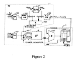
- FIG. 2 is a circuit block diagram of an embodiment of the present invention.
- the circuit applies a local high-speed crystal oscillator providing an oscillator frequency of 58.32 MHz to recover an ideal 2.048 MHz clock with minimized vibration, and the phase accumulator 3 applies a 24-bit adder.
- FIFO first-in-first-out memory
- the digital signal Dif-int representing the integer part of the detected phase difference ⁇ is then fed to the loop filter 2.
- a digital signal Dif-frac representing the fractional part of the detected phase difference ⁇ which is also fed to the loop filter 2, is given by the signal Sum (23:21), which represents the sum of accumulated phase values stored in the three most significant bits of the digital signal supplied by the phase accumulator 3.
- the loop filter 2 calculates, according to a method described in detail below, the input signal K(x) of the phase accumulator 3 based on a digital signal x represented by a function of two further digital signals Dif-int and Dif-frac representing the integer part and the fractional part of the detected phase difference ⁇ , respectively, and outputs the calculated data to the phase accumulator 3 which performs an accumulation procedure.
- the clock frequency of the phase sampling module 105 is the frequency of the clock signal Fmclk synchronized by a local high-speed crystal oscillator Clk58m.
- Fmclk is a sampling clock signal which appears at a specific position of the frame head of each frame.
- the phase accumulator 3 accumulates the output signal K ( x ) of the loop filter 2 on each rising clock edge of the clock signal Clk58m supplied by the local high-speed crystal oscillator.
- the carry bit of addition is automatically overflowed, and the addition sum is stored to the register output variable Sum (23:0) on each rising clock edge of Clk58m.
- the accumulated phase values stored in the most significant bit Sum (23) of the digital signal supplied by the phase accumulator 3 thereby represents the local recovery clock signal Rclk.
- the loop filter 2 implements an operational function for calculating the accumulated signal K ( x ) and adjusts the local recovery clock signal frequency f rec at the output port of the phase accumulator 3.
- the operational method according to one aspect of the invention is as follows: First, an address difference reference offset x 0 representative of said phase difference reference value ⁇ ref is set to half the bit depth L of the first-in-first-out (FIFO) memory 101 for defining a phase difference reference value ⁇ ref representing a nominal value of the difference ⁇ between the phase ⁇ ref of the input clock signal Wclk and the phase ⁇ rec of the local recovery clock signal Rclk.
- Subtracter module 104 calculates the phase difference ⁇ between the input clock signal phase ⁇ ref and the local recovery clock signal phase ⁇ rec according to the obtained output signal Waddr(6:0) of the write address counter 102 and the obtained output signal Raddr(6:0) of the read address counter 103, and the obtained calculation result Dif-intO, after being submitted to a sampling procedure with the clock signal Fmclk, is sent to the loop filter 2 as a digital signal Dif-int representing an integer part of the detected phase difference ⁇ .
- the write clock of the FIFO 101 is given by the input clock signal Wclk after being synchronized by the local high-speed crystal oscillator clock signal Clk58m, and the read clock of the FIFO 101 is given by the local recovery clock signal Rclk.
- the phase accumulator 3 outputs to said phase sampling module 105 a digital signal Dif-frac(2:0) constituted by the sum Sum (23:21) of the digital values stored in the three most significant bits of 24-bit register 302.
- the digital signal Dif-frac(2:0) after being submitted to a phase sampling procedure with clock signal Fmclk, is fed to the loop filter 2 as a fractional part of the phase difference representing signal x.
- the loop filter 2 calculates the accumulated signal K ( x ) in segments according to a deviation of the detected phase difference ⁇ represented by the digital signal x (in bit) and a phase dif ference reference value ⁇ ref represented by an address difference reference offset x 0 of 64 bit.
- the accumulated signal K ( x ) follows x with a larger increment ⁇ Km; when said deviation is small, the accumulated signal K ( x ) follows x with a smaller increment ⁇ Km .
- the accumulated signal K ( x ) is then fed to the phase accumulator 3 for accumulation.
- the accumulated input signal K (x) in each segment follows the detected phase difference ⁇ with a continuous, piecewise linear and strictly monotonously rising function, said function featuring the four segment slope factors ⁇ 0 , ⁇ 1 , ⁇ 2 , and ⁇ 3 ⁇ R, respectively, with ⁇ 0 , ⁇ 1 , ⁇ 2 and ⁇ 3 obeying the inequation ⁇ 0 ⁇ ⁇ 1 ⁇ ⁇ 2 ⁇ ⁇ 3 .
- bit depth L of FIFO 101 is 128 bit
- x can take values from a range between 0 and 128 bit.
- FIG. 3 shows that the above-mentioned accumulator input signal K (x) is a continuous, piecewise linear and strictly monotonously rising function of digital signal x .
- K ( x ) is implemented without error code and, at the same time, vibration minimization is also concerned, such that DPLL vibration tolerance is better raised, vibration transfer characteristic is enhanced, and net output vibration indicators at low-band and high-band frequencies are improved.
- vibration tolerance is given by 60 UI (units of issue) and vibration suppression characteristic is higher than -30 dB; when reference clock frequency is 2,018 kHz, net output vibration is less than 0.1 UI, and when reference clock frequency is 18,100 kHz, net output vibration is 0.035 UI in general.
Landscapes
- Engineering & Computer Science (AREA)
- Computer Networks & Wireless Communication (AREA)
- Signal Processing (AREA)
- Stabilization Of Oscillater, Synchronisation, Frequency Synthesizers (AREA)
- Manipulation Of Pulses (AREA)
- Synchronisation In Digital Transmission Systems (AREA)
Abstract
Description
- The present invention generally relates to digital phase-locked loop (DPLL) frequency synthesizer technology and, more particularly, to a method for controlling the phase and stabilizing the output frequency of a local crystal oscillator clock signal by means of a DPLL frequency synthesizer circuitry.
- A phase-locked loop (PLL) frequency synthesizer circuitry is realized as a closed-loop tracking system which is able to track the phase and frequency of a given input signal. When a PLL frequency synthesizer circuitry tracks an input signal with constant frequency, there is no frequency difference. By contrast, when a PLL frequency synthesizer circuitry is used to track an input signal with variable frequency, deviations of an oscillator signal frequency from a given reference frequency are detected and compensated. Thereby, tracking accuracy is very high.
- There are two kinds of phase-locked loop circuitries: analog PLL circuitries (APLL) and digital PLL circuitries (DPLL). An APLL frequency synthesizer circuitry consists of a phase detector (PD), a loop filter (LF) as well as a voltage-controlled oscillator (VCO). Compared with a DPLL frequency synthesizer circuitry, an APLL frequency synthesizer circuitry has better vibration suppression performance but features discreteness in technology and involves higher manufacturing costs and lower stability.
- If a part of a DPLL frequency synthesizer circuitry is realized as a digital circuit, said DPLL frequency synthesizer circuitry is called partial DPLL circuitry. The herein applied principle is similar to an APLL frequency synthesizer circuitry, and as its frequency control still applies an analog circuitry, a partial DPLL circuitry also implies the drawback of high discreteness, difficulties in manufacturing and high manufacturing costs. In contrast thereto, a so-called all-digital phase-locked loop (DPLL) circuitry is realized by digital circuit elements only.
- A new implementation method of a DPLL frequency synthesizer circuitry is disclosed in US 5,033,064. The DPLL frequency synthesizer circuitry implemented by this method features better vibration transfer characteristics and net vibration output characteristics, but there is no effective loop filtering method, and vibration filter performance at lower band frequencies is not ideal.
- US 5,793,824 describes a bandwidth-adaptive digital phase locked loop (DPLL)-based clock control arrangement for pulse stuffing a synchronized digital communication system, wherein said DPLL-based clock control arrangement controls the generation of a read-out clock signal which is used for retiming a digital data signal interfaced with a synchronous data channel of said communication system, in which pulse-stuffing synchronization is employed to maintain clock synchronization of the asynchronous digital data signal with a synchronous digital data channel over which the digital data signal is transported. The bandwidth-adaptive digital phase locked loop thereby comprises a loop filter to which an error signal representative of a difference between the asynchronous digital data and a reference clock signal is applied and a phase accumulator which is coupled to the output port of said loop filter and being operative to stepwise adjust the read-out clock signal. The loop filter features a first scaled path having a first, controllably stepped amplification stage as well as a second scaled path having a second, controllably stepped amplification stage coupled to a frequency accumulator. The output signals of the frequency accumulator and said first stepped amplification stage are summed and coupled to the phase accumulator. According to one embodiment of the invention disclosed in US 5,793,824, gain values of each of the first and second amplification stages are incrementally adjusted in accordance with the magnitude of the error signal.
- In
EP 0 584 627 A2 an incremental phase smoothing desynchronizer and calculation apparatus for desynchronizing data stored within synchronous payload envelopes of a synchronous communication protocol such as SONET (Synchronous Optical Network), said desynchronizer comprising a partial DPLL frequency synthesizer circuitry used for tracking the phase and frequency of an oscillator output signal, is described which provides for smoothing a periodically discontinuous clock signal associated with said data after a synchronous communication protocol overhead has been removed. The desynchronizer accommodates for shifts in the position of said payload envelope and, hence, the data within the synchronous communication frame as well as adjustments within said data itself due to asynchronous bit stuff information. It thereby comprises a leak filter having a linear branch and an integrator branch, both branches having adjustable factors regarding their operation, wherein the adjustable factors are selected depending on threshold values which in turn are based on the difference between an average write address and a read address of an elastic store within which incoming data removed from the aforementioned synchronous communication system frame is temporarily stored. The leak filter constitutes one part of a phase-locked loop which is used for adjusting a read clock frequency in a manner which minimizes overflow or underflow of the elastic store while simultaneously minimizing the changing rate of the read clock rate so as to limit jitter. A fault recovery apparatus constitutes a part of the desynchronizer that is used for enabling a fast lock of high gain factors to quickly adjust said read clock frequency in case an overflow or underflow of the elastic store occurs. - The present invention is basically dedicated to a method for controlling the phase ϕ LO and stabilizing the output frequency f LO of a local crystal oscillator clock signal by means of a digital phase-locked loop (DPLL) frequency synthesizer circuitry. Said method is characterized by the steps of defining a phase difference reference value Δϕ ref representing a nominal value of the difference Δϕ between the phase ϕ ref of an input clock signal and the phase ϕ rec of a local recovery clock signal by setting an address difference reference offset x 0 representative of said phase difference reference value Δϕ ref to half the bit depth L of the first-in-first-out memory, calculating a read/write address difference which denotes a bit position difference in a data stream of contents data between an input data pointer and an output data pointer referring to the starting addresses of contents data written to and contents data read from the first-in-first-out memory, respectively, said read/write address difference being representative of a detected phase difference Δϕ between the input clock signal and the local recovery clock signal, comparing the detected phase difference Δϕ with the phase difference reference value Δϕ ref , and adjusting the local recovery clock signal in segments to the phase difference reference value Δϕ ref , wherein a correction signal K(x) which is used for adjusting the local recovery clock signal, said correction signal being representative of a change in the detected phase difference Δϕ, is increased or decreased segment by segment depending on the magnitude and the algebraic sign of a detected deviation of the detected phase difference Δϕ from the phase difference reference value Δϕ ref .
- According to one aspect of the invention, the first-in-first-out memory receives a write address signal and a read address signal, the write address signal being a counter output value representative of the clock frequency of the input clock signal synchronized with a local crystal oscillator clock signal and the read address signal being a further counter output value representative of the clock frequency f rec of the local recovery clock signal.
- According to another aspect of the present invention, said step of adjusting the local recovery clock signal in segments comprises the steps of sampling the detected phase difference Δϕ, calculating increments ΔK m of a phase accumulator input signal K(x) that is used for adjusting the phase ϕ rec of the local recovery clock signal based on a deviation of a sampled time-domain signal representing the detected phase difference Δϕ from the phase difference reference value Δϕ ref such that in case said deviation increases the step size of said increments ΔK m is set to a larger value, whereas in case said deviation decreases the step size of said increments ΔK m is set to a smaller value, said increments being a function of the sampled time-domain signal representing the detected phase difference Δϕ, wherein an integer part of the detected phase difference Δϕ is given by the read/write address difference and a digital signal representing the fractional part of the detected phase difference Δϕ is given by a particular increment ΔK m or by a partial sum of said increments ΔK m . The aforementioned step of adjusting the local recovery clock signal in segments also comprises the steps of accumulating said increments ΔK m and calculating said local recovery clock signal by controlling the divider coefficient of a digital frequency divider used for dividing the frequency f LO of the local crystal oscillator clock signal such that in case said deviation increases an offset rate used for adjusting the phase ϕ rec of the local recovery clock signal to the phase ϕ ref of the input clock signal is set to a larger value, whereas in case said deviation decreases said offset rate is set to a smaller value, said offset rate being a cumulative function of digital signals being representative of the frequency f LO of said local crystal oscillator clock signal divided by different divider coefficients stored in the digital frequency divider.
- The steps of accumulating said increments ΔK m and calculating said local recovery clock signal are thereby performed by means of a phase accumulator comprising an adder and a register supplied with a signal being representative of the frequency f LO of the local crystal oscillator clock signal.
- According to a further aspect of the invention, said step of sampling the detected phase difference Δϕ is performed by means of a phase sampling module supplied with a sampling clock signal which is synchronized by the local crystal oscillator clock signal.
- According to a still further aspect of the present invention, the phase accumulator input signal K(x) is a continuous, piecewise linear and strictly monotonously rising function of a digital signal x, wherein x is given by a function of two further digital signals representing said integer part and said fractional part of the detected phase difference Δϕ, respectively.
- According to a still further aspect of the present invention, the bit depth L of the first-in-first-out memory is given by 128 bit and the phase difference reference value Δϕ ref is represented by an address difference reference offset x0 of 64 bit.
- Because the invention is based on a DPLL circuitry, it is able to overcome weaknesses of conventional APLL circuitries, which include large dispersion, high cost and low stability. The local recovery clock signal frequency f rec , which is supplied by the digital frequency divider, can adaptively be adjusted according to the detected phase difference Δϕ.
- In the following description preferred embodiments of the present invention are explained in more detail with reference to the enclosed drawings. Thereby,
- FIG. 1
- shows a block diagram of a DPLL circuitry according to the present invention,
- FIG. 2
- shows a more detailed view of the block diagram depicted in Fig. 1, and
- FIG. 3
- depicts a function diagram showing the input signal K(x) of the phase accumulator as a function of a digital signal x represented by a function of the integer part and the fractional part of the detected phase difference Δϕ.
- The present invention will now be described in more detail with reference to the accompanying drawings, in which preferred embodiments of the invention are shown. This invention may, however, be embodied in many different forms and should not be construed as limited to the embodiments set forth herein; rather, these embodiments are provided such that the disclosure will be thorough and complete and will fully convey the scope of the invention to those skilled in the art. Thereby, like reference numbers refer to like elements throughout.
- FIG. 1 shows that a DPLL generally comprises a phase detector 1, a loop filter (loop filter) 2 and a
phase accumulator 3. The phase detector 1 receives an input clock signal Wclk and a local recovery clock signal Rclk, performs frequency detection and phase detection, and outputs a phase difference Δϕ to theloop filter 2. Theloop filter 2 calculates an accumulated frequency signal K(x) according to a signal x representing the phase difference Δϕ. Thephase accumulator 3 comprises anadder 301 and aregister 302 which serves as a frequency divider. Theadder 301 adds output data S of theregister 302 and output data K of theloop filter 2, and theregister 302 stores the current adding result at every rising clock pulse edge of a local high-speed crystal oscillator signal. Typically, the register has a bit length that equals the adder bit length, and the register only stores a sum without carry bit. Theregister 302 outputs to theadder 301 an accumulated value S(n:0), e.g. the result of last adding, such that a cumulative function is implemented. The variable 'n' herein represents the adder bit length, and the most significant bit (MSB) of the accumulative value is a local recovery clock signal frequency f rec recovered by thephase accumulator 3 whose output is provided to the phase detector 1 for phase detection. The clock frequency of thephase accumulator 3 is thereby given by the local high-speed crystal oscillator's frequency f LO . - FIG. 2 is a circuit block diagram of an embodiment of the present invention. The circuit applies a local high-speed crystal oscillator providing an oscillator frequency of 58.32 MHz to recover an ideal 2.048 MHz clock with minimized vibration, and the
phase accumulator 3 applies a 24-bit adder. The digital phase detector 1, which is integrated into a DPLL circuitry, performs frequency detection and phase detection and comprises a first-in-first-out memory (FIFO) 101 with a bit depth of L = 128 bit, aread address counter 103 and awrite address counter 102, asubtracter module 104, aphase sampling module 105 and twosynchronization circuits subtracter module 104 thereby calculates a read/write address difference Dif-int0 which is representative of a digital signal Dif-int representing an integer part of the detected phase difference Δϕ, wherein Dif-int is given by the read/write address difference Dif-int0(6:0) := Waddr(6:0) - Raddr(6:0) after being sampled by a sampling clock signal Fmclk. The digital signal Dif-int representing the integer part of the detected phase difference Δϕ is then fed to theloop filter 2. - A digital signal Dif-frac representing the fractional part of the detected phase difference Δϕ, which is also fed to the
loop filter 2, is given by the signal Sum(23:21), which represents the sum of accumulated phase values stored in the three most significant bits of the digital signal supplied by thephase accumulator 3. Theloop filter 2 calculates, according to a method described in detail below, the input signal K(x) of thephase accumulator 3 based on a digital signal x represented by a function of two further digital signals Dif-int and Dif-frac representing the integer part and the fractional part of the detected phase difference Δϕ, respectively, and outputs the calculated data to thephase accumulator 3 which performs an accumulation procedure. The clock frequency of thephase sampling module 105 is the frequency of the clock signal Fmclk synchronized by a local high-speed crystal oscillator Clk58m. Thereby, Fmclk is a sampling clock signal which appears at a specific position of the frame head of each frame. Thephase accumulator 3 accumulates the output signal K(x) of theloop filter 2 on each rising clock edge of the clock signal Clk58m supplied by the local high-speed crystal oscillator. The carry bit of addition is automatically overflowed, and the addition sum is stored to the register output variable Sum(23:0) on each rising clock edge of Clk58m. The accumulated phase values stored in the most significant bit Sum(23) of the digital signal supplied by thephase accumulator 3 thereby represents the local recovery clock signal Rclk. - The
loop filter 2 implements an operational function for calculating the accumulated signal K(x) and adjusts the local recovery clock signal frequency f rec at the output port of thephase accumulator 3. The operational method according to one aspect of the invention is as follows: First, an address difference reference offset x 0 representative of said phase difference reference value Δϕ ref is set to half the bit depth L of the first-in-first-out (FIFO)memory 101 for defining a phase difference reference value Δϕ ref representing a nominal value of the difference Δϕ between the phase ϕ ref of the input clock signal Wclk and the phase ϕ rec of the local recovery clock signal Rclk. In this embodiment, a FIFO with a bit depth L of 128 bit is applied, such that the address difference reference offset x 0 can be set to x 0 := L / 2 = 128 bit / 2 = 64 bit.Subtracter module 104 then calculates the phase difference Δϕ between the input clock signal phase ϕ ref and the local recovery clock signal phase ϕ rec according to the obtained output signal Waddr(6:0) of thewrite address counter 102 and the obtained output signal Raddr(6:0) of the readaddress counter 103, and the obtained calculation result Dif-intO, after being submitted to a sampling procedure with the clock signal Fmclk, is sent to theloop filter 2 as a digital signal Dif-int representing an integer part of the detected phase difference Δϕ. The write clock of theFIFO 101 is given by the input clock signal Wclk after being synchronized by the local high-speed crystal oscillator clock signal Clk58m, and the read clock of theFIFO 101 is given by the local recovery clock signal Rclk. Thephase accumulator 3 outputs to said phase sampling module 105 a digital signal Dif-frac(2:0) constituted by the sum Sum(23:21) of the digital values stored in the three most significant bits of 24-bit register 302. The digital signal Dif-frac(2:0), after being submitted to a phase sampling procedure with clock signal Fmclk, is fed to theloop filter 2 as a fractional part of the phase difference representing signal x. - The
loop filter 2 calculates the accumulated signal K(x) in segments according to a deviation of the detected phase difference Δϕ represented by the digital signal x (in bit) and a phase dif ference reference value Δϕ ref represented by an address difference reference offset x0 of 64 bit. When the deviation |x - x 0| is large, the accumulated signal K(x) follows x with a larger increment ΔKm; when said deviation is small, the accumulated signal K(x) follows x with a smaller increment ΔKm. The accumulated signal K(x) is then fed to thephase accumulator 3 for accumulation. Therefore, when |x - x 0| increases, the frequency of the local recovery clock signal Rclk, i.e. the most significant bit Sum(23), is changed towards the nominal ideal frequency 2.048 MHz with a higher rate; otherwise, when |x - x 0| decreases, the frequency of the local recovery clock signal Rclk is changed towards the nominal ideal frequency 2.048 MHz with a lower rate. - According to one embodiment of the present invention, the loop filter 2 applies seven increments ΔK 1, ΔK 2 , ..., ΔK 7 and four coefficients α1, α2 , ... α4 to an algorithm used for calculating the phase accumulator input signal K(x) according to the magnitude and the algebraic sign of a measured deviation (x - x 0) representing a deviation of the detected phase difference Δϕ from the phase difference reference value Δϕ ref , wherein said algorithm is given by the following function:


with Δx := 16 bit and x 0 := 4-Δ= 64 bit, wherein
with ΔA wR (n·T s ) being address difference Dif-int0, β1, and β2 being real-valued spreading factors used for spreading the obtained values for Dif-int and Dif-frac (here: β1 = β2 := 1),
being the respective frequency divider coefficient given by the binary value ('0' or 1') stored in the l-th bit cell ofregister 302, which follows from the fact that a digital value represented by a bit sequence B := (b 0 , b 1 , b 2 , ..., b 1 , ..., b Lreg ) which is stored in saidregister 302 is representative of a sequence of frequency divider coefficients c l which can be written in the form
L reg := 24 bit being the bit depth ofregister 302, L s being the index of the L s -th bit cell of saidregister 302,
being the address difference reference offset and, finally, L being the bit depth of first-in-first-out memory 101 denotes a digital signal being a function of two further digital signals Dif-int and Dif-frac which are representative of the integer part and the fractional part of the detected phase difference Δϕ, respectively, said function containing a shift of the obtained address difference signal by the address difference reference offset xo, K 0 is a digital reference value of the phase accumulator input signal K(x) supplied by theloop filter 2 when the detected phase difference Δϕ is equal to the phase difference reference value Δϕ ref , K 0 being calculated dependent on the frequency f rec of the local recovery clock signal Rclk, the frequency f LO of the local crystal oscillator signal and the bit depth L reg ofregister 302, which is obtained when x is equal to x 0, and m is the index of said increments ΔK m . The accumulated input signal K(x) in each segment follows the detected phase difference Δϕ with a continuous, piecewise linear and strictly monotonously rising function, said function featuring the four segment slope factors α0, α1, α2, and α3 ∈ R, respectively, with α0, α1, α2 and α3 obeying theinequation 
- Thereby, said segment slope factors α0, α1, a and α3 are respectively set to the following values: α0 := 1, α1 := 2, α2 := 3, and α3 := 4.
- According to the above-described embodiment of the present invention, the phase accumulator input value K 0 supplied by
loop filter 2 in case x is equal to x 0 is given by the following equation:
- Due to the fact that in the above-described embodiment the bit depth L of
FIFO 101 is 128 bit, x can take values from a range between 0 and 128 bit. - FIG. 3 shows that the above-mentioned accumulator input signal K(x) is a continuous, piecewise linear and strictly monotonously rising function of digital signal x. At segments where x deviates farthest from x 0 = 64 bit, such as at
bit segments 0 < x ≤ 16 bit and 112 < x ≤ 128 bit having the steepest slope factor of all segments, the accumulated signal K(x) follows x with largest increments ΔK m , from which it follows that the frequency f rec of local recovery clock signal Rclk is adjusted to a nominal frequency given by the clock frequency f ref = 2.048 MHz of input clock signal Wclk with fastest changing rate. At segments where x deviates largely from x 0 = 64 bit, such as atbit segments 16 < x ≤ 32 bit and 96 < x ≤ 112 bit, where the slope factors of the segments are relatively steep, the accumulated signal K(x) follows x with relatively large increments ΔK m , compared with the increment values at other segments, which implies that f rec is adjusted to f ref = 2.048 MHz with a relatively fast changing rate. By contrast, at segments where x deviates less from x 0 = 64 bit, such as atbit segments 32 < x ≤ 48 bit and 80 < x ≤ 96 bit, where the slope factors of the segments are relatively small, the accumulated signal K(x) follows x with relatively small increments ΔK m , compared with the increment values at other segments, which leads to the fact that f rec is adjusted to f ref = 2.048 MHz with a relatively slow changing rate. Finally, at the segment where the magnitude of the deviation (x - x 0) features a minimum, such as atbit segment 48 < x ≤ 80 bit having the smallest slope factor of all segments, the accumulated signal K(x) follows x with smallest increments ΔK m , from which it follows that f rec is adjusted to f ref = 2.048 MHz with slowest changing rate. Thereby, K(x) is implemented without error code and, at the same time, vibration minimization is also concerned, such that DPLL vibration tolerance is better raised, vibration transfer characteristic is enhanced, and net output vibration indicators at low-band and high-band frequencies are improved. In the embodiment discussed above, when reference clock frequency is 20 Hz, vibration tolerance is given by 60 UI (units of issue) and vibration suppression characteristic is higher than -30 dB; when reference clock frequency is 2,018 kHz, net output vibration is less than 0.1 UI, and when reference clock frequency is 18,100 kHz, net output vibration is 0.035 UI in general.
Claims (10)
- A method for controlling the phase (ϕ LO ) and stabilizing the output frequency (f LO ) of a local crystal oscillator clock signal (Clk58m) by means of a digital phase-locked loop (DPLL) frequency synthesizer circuitry, said method comprising the steps of- defining a phase difference reference value (Δϕ ref ) representing a nominal value of the difference (Δϕ) between the phase (ϕ ref ) of an input clock signal (Wclk) and the phase (ϕ rec ) of a local recovery clock signal (Rclk) by setting an address difference reference offset (x 0) representative of said phase difference reference value (Δϕ ref ) to half the bit depth (L) of a the first-in-first-out memory (101),- calculating a read/write address difference (Dif-int0) which denotes a bit position difference in a data stream of contents data between an input data pointer (Pw) and an output data pointer (PR) indicating the starting addresses of contents data (Wdata) written to and contents data (Rdata) read from the first-in-first-out memory (101), respectively, said read/write address difference (Dif-int0) being representative of a detected phase difference (Δϕ) between the input clock signal (Wclk) and the local recovery clock signal (Rclk),- comparing the detected phase difference (Δϕ) with the phase difference reference value (Δϕ ref ), and- adjusting the local recovery clock signal (Rclk) in segments to the phase difference reference value (Δϕ ref ), wherein a correction signal (K(x)) used for adjusting the local recovery clock signal (Rclk), said correction signal (K(x)) being representative of a change in the detected phase difference (Δϕ), is increased or decreased segment by segment depending on the magnitude and the algebraic sign of a detected deviation of the detected phase difference (Δϕ) from the phase difference reference value (Δϕ ref ),characterized in that
said correction signal (K(x)) is calculated based on a digital signal (x) which, compared with said read/write address difference (Dif-int0), is representative of a more precise representation of the detected phase difference (Δϕ), said digital signal (x) being a function of two further digital signals (Dif-int and Dif-frac) representing an integer part and a fractional part of the detected phase difference (Δϕ), respectively. - The method according to claim 1,
characterized in that
the digital signal (Dif-int) representing the integer part of the detected phase difference (Δϕ) is given by the read/write address difference (Dif-int0) and the digital signal (Dif-frac) representing the fractional part of the detected phase difference (Δϕ) is given by a particular increment (ΔK m ) of said correction signal (K(x)) or by a partial sum of said increments (ΔK m ). - The method according to claim 2,
characterized in that
the first-in-first-out memory (101) receives a write address signal (Waddr) and a read address signal (Raddr), the write address signal (Waddr) being a counter output value which is representative of the clock frequency of the input clock signal (Wclk) synchronized with a local crystal oscillator clock signal (Clk58m) and the read address signal (Raddr) being a further counter output value which is representative of the clock frequency (f rec ) of the local recovery clock signal (Rclk). - The method according to claim 3,
characterized in that the step of adjusting the local recovery clock signal (Rclk) in segments comprises the steps of- sampling (105) the detected phase difference (Δϕ),- calculating (2) increments (ΔK m ) of a phase accumulator input signal (K(x)) which is used for adjusting the phase (ϕ rec ) of the local recovery clock signal (Rclk) based on a deviation of a sampled time-domain signal representing the detected phase difference (Δϕ) from the phase difference reference value (Δϕ ref ) such that in case said deviation increases the step size of said increments is set to a larger value, whereas in case said deviation decreases the step size of said increments (ΔK m ) is set to a smaller value, said increments (ΔK m ) being a function of the sampled time-domain signal representing the detected phase difference (Δϕ),- accumulating (301) said increments (ΔK m ), and- calculating (302) said local recovery clock signal (Rclk) by controlling the divider coefficient of a digital frequency divider (302) used for dividing the frequency (f LO ) of the local crystal oscillator clock signal (Clk58m) such that in case said deviation increases an offset rate used for adjusting the phase (ϕ rec ) of the local recovery clock signal (Rclk) to the phase (ϕ ref ) of the input clock signal (Wclk) is set to a larger value, whereas in case said deviation decreases said offset rate is set to a smaller value, said offset rate being a cumulative function of digital signals which are representative of the frequency (f LO ) of said local crystal oscillator clock signal (Clk58m) divided by different divider coefficients stored in the digital frequency divider (302). - The method according to claim 4,
characterized in that
the steps of accumulating (301) said increments (ΔK m ) and calculating (302) said local recovery clock signal (Rclk) are performed by means of a phase accumulator (3) comprising an adder (301) and a register (302) supplied with a signal being representative of the frequency (f LO ) of the local crystal oscillator clock signal (Clk58m). - The method according to claim 5,
characterized in that
the step of sampling (105) the detected phase difference (Δϕ) is performed by means of a phase sampling module (105) supplied with a sampling clock signal (Fmclk) which is synchronized by the local crystal oscillator clock signal (Clk58m). - The method according to claim 6,
characterized in that
the phase accumulator input signal (K(x)) is a continuous, piecewise linear and strictly monotonously rising function of the digital signal (x) which is representative of the more precise representation of the detected phase difference (Δϕ). - The method according to claim 7,
characterized in that
the bit depth (L) of the first-in-first-out memory (101) is given by 128 bit and the phase difference reference value (Δϕref) is represented by an address difference reference offset (x 0) of 64 bit. - The method according to claim 8,
characterized in that
in the step of calculating (2) increments (ΔK m ) of a phase accumulator input signal (K(x)) seven increments (ΔK 1, ΔK 2, ..., ΔK 7) and four coefficients (α1, α2, ... α4) are applied to an algorithm used for calculating the phase accumulator input signal (K(x)) according to the deviation of the sampled time-domain signal representing the detected phase difference (Δϕ) from the phase difference reference value (Δϕ ref ), wherein said algorithm is given by the following function:


Δx := 16 bit and x 0 := 4·Δx = 64 bit, wherein x (in bit) is a digital signal which is represented by a function of two further digital signals (Dif-int and Dif-frac) which are representative of the integer part and the fractional part of the detected phase difference (Δϕ), K 0 denotes a digital reference value of the phase accumulator input signal (K(x)) which is obtained when the detected phase difference (Δϕ) is equal to the phase difference reference value (Δϕ ref ), K 0 being calculated dependent on the frequency (f rec ) of the local recovery clock signal (Rclk), the frequency (f LO ) of the local crystal oscillator signal (Clk58m) and the bit depth (L reg ) of said register (302), and m is the index of said increments (ΔK m ), and wherein the accumulated input signal (K(x)) in each segment follows the detected phase difference (Δϕ) with a continuous, piecewise linear and strictly monotonously rising function, said function having the segment slope factors α0, α1 , α 2 , α 3 ∈ R, respectively, with α0, α1 , α2 and α3 obeying the inequation α0 < α1 , < α 2 < α3 . - The method according to claim 9,
characterized in that
said segment slope factors α0, α1 , α2 and α3 are set to the following values: α0 := 1, α 1 := 2, α 2 := 3, and α3 := 4.
Applications Claiming Priority (3)
| Application Number | Priority Date | Filing Date | Title |
|---|---|---|---|
| CN00101582 | 2000-01-27 | ||
| CN00101582.6A CN1307406A (en) | 2000-01-27 | 2000-01-27 | Filtering method of digital phase lock loop |
| PCT/CN2001/000068 WO2001059931A1 (en) | 2000-01-27 | 2001-01-20 | Method for filtering used in a digital phase locked loop |
Publications (3)
| Publication Number | Publication Date |
|---|---|
| EP1253719A1 EP1253719A1 (en) | 2002-10-30 |
| EP1253719A4 EP1253719A4 (en) | 2004-10-20 |
| EP1253719B1 true EP1253719B1 (en) | 2006-08-16 |
Family
ID=4576075
Family Applications (1)
| Application Number | Title | Priority Date | Filing Date |
|---|---|---|---|
| EP01903571A Expired - Lifetime EP1253719B1 (en) | 2000-01-27 | 2001-01-20 | Method for filtering used in a digital phase locked loop |
Country Status (9)
| Country | Link |
|---|---|
| US (1) | US6819730B2 (en) |
| EP (1) | EP1253719B1 (en) |
| CN (1) | CN1307406A (en) |
| AT (1) | ATE336826T1 (en) |
| AU (1) | AU2001231482A1 (en) |
| BR (1) | BR0107891A (en) |
| CA (1) | CA2398596C (en) |
| DE (1) | DE60122287D1 (en) |
| WO (1) | WO2001059931A1 (en) |
Families Citing this family (22)
| Publication number | Priority date | Publication date | Assignee | Title |
|---|---|---|---|---|
| TWI220843B (en) * | 2002-04-01 | 2004-09-01 | Mstar Semiconductor Inc | Apparatus and method of clock recovery for sampling analog signals |
| US7184508B2 (en) * | 2002-12-23 | 2007-02-27 | Sun Microsystems, Inc. | Capturing data and crossing clock domains in the absence of a free-running source clock |
| GB2398942A (en) * | 2002-12-30 | 2004-09-01 | Nokia Corp | Phase locked loop with delay circuit |
| US6774732B1 (en) * | 2003-02-14 | 2004-08-10 | Motorola, Inc. | System and method for coarse tuning a phase locked loop (PLL) synthesizer using 2-PI slip detection |
| KR100493106B1 (en) * | 2003-05-21 | 2005-06-02 | 삼성전자주식회사 | apparatus for receiving asynchronous transmission stream in digital broadcasting receiver according to DVB-ASI and method for processing asynchronous transmission stream thereof |
| GB2409383B (en) * | 2003-12-17 | 2006-06-21 | Wolfson Ltd | Clock synchroniser |
| GB2413043B (en) * | 2004-04-06 | 2006-11-15 | Wolfson Ltd | Clock synchroniser and clock and data recovery apparatus and method |
| CN100481728C (en) * | 2004-07-05 | 2009-04-22 | 友达光电股份有限公司 | Clock data recovery device and method for low voltage differential signal |
| TWI281789B (en) * | 2004-12-10 | 2007-05-21 | Via Tech Inc | Phase lock loop device |
| US7646836B1 (en) * | 2005-03-01 | 2010-01-12 | Network Equipment Technologies, Inc. | Dynamic clock rate matching across an asynchronous network |
| US7224638B1 (en) | 2005-12-15 | 2007-05-29 | Sun Microsystems, Inc. | Reliability clock domain crossing |
| US7627065B2 (en) * | 2005-12-21 | 2009-12-01 | Sun Microsystems, Inc. | Generating a clock crossing signal based on clock ratios |
| US8331512B2 (en) | 2006-04-04 | 2012-12-11 | Rambus Inc. | Phase control block for managing multiple clock domains in systems with frequency offsets |
| CN100464503C (en) * | 2006-09-12 | 2009-02-25 | 威盛电子股份有限公司 | Method and apparatus for adjusting clock signal |
| CN101083523B (en) * | 2007-07-27 | 2010-08-11 | 华南理工大学 | A method and device for implementing integrated time stamp clock synchronous phase-locked loop |
| KR100994128B1 (en) * | 2008-09-23 | 2010-11-15 | 한국전자통신연구원 | Method and device for time stamping for high precision network synchronization |
| KR20120114214A (en) * | 2009-11-25 | 2012-10-16 | 신포니아 테크놀로지 가부시끼가이샤 | Vibration damping device and vehicle provided therewith |
| TWI435596B (en) * | 2010-07-06 | 2014-04-21 | Realtek Semiconductor Corp | Master/slave decision device and master/slave decision method applied to network device |
| US8959469B2 (en) | 2012-02-09 | 2015-02-17 | Altera Corporation | Configuring a programmable device using high-level language |
| US9052900B2 (en) | 2013-01-29 | 2015-06-09 | Oracle International Corporation | Serdes fast retrain method upon exiting power saving mode |
| US20180186546A1 (en) * | 2016-12-29 | 2018-07-05 | Dow Global Technologies Llc | Packaging with Three-Dimensional Loop Material |
| CN107707263A (en) * | 2017-08-04 | 2018-02-16 | 上海航天电子有限公司 | Adapt to the universal integrated remote measurement ground checkout equipment of wide scope code check |
Family Cites Families (20)
| Publication number | Priority date | Publication date | Assignee | Title |
|---|---|---|---|---|
| US3992580A (en) * | 1975-04-24 | 1976-11-16 | The United States Of America As Represented By The Secretary Of The Army | Discrete control correction for synchronizing digital networks |
| CA1262173A (en) * | 1986-05-29 | 1989-10-03 | James Angus Mceachern | Synchronization of asynchronous data signals |
| US4941156A (en) * | 1987-05-19 | 1990-07-10 | Crystal Semiconductor | Linear jitter attenuator |
| US5033064A (en) * | 1988-12-09 | 1991-07-16 | Transwitch Corporation | Clock dejitter circuit for regenerating DS1 signal |
| US4942593A (en) * | 1989-03-16 | 1990-07-17 | Dallas Semiconductor Corporation | Telecommunications interface with improved jitter reporting |
| JPH03157018A (en) | 1989-08-10 | 1991-07-05 | Mitsubishi Electric Corp | Frequency synthesizer |
| US5036294A (en) * | 1990-12-03 | 1991-07-30 | Motorola Inc. | Phase locked loop having low-frequency jitter compensation |
| US5638411A (en) * | 1991-05-23 | 1997-06-10 | Mitsubishi Denki Kabushiki Kaisha | Stuff bit synchronization system |
| JP2776098B2 (en) * | 1991-11-27 | 1998-07-16 | 松下電器産業株式会社 | Clock recovery circuit and time axis error correction device |
| US5402452A (en) * | 1992-08-25 | 1995-03-28 | Alcatel Network Systems, Inc. | Incremental phase smoothing desynchronizer and calculation apparatus |
| KR100312623B1 (en) * | 1993-02-26 | 2001-12-28 | 이데이 노부유끼 | Active filter circuit device |
| FR2709623B1 (en) * | 1993-08-31 | 1995-11-17 | Sgs Thomson Microelectronics | Digital phase locked loop filter. |
| DE4336239A1 (en) * | 1993-10-23 | 1995-04-27 | Sel Alcatel Ag | Circuit arrangement for a clock generator |
| US5633898A (en) * | 1993-12-22 | 1997-05-27 | Matsushita Electric Industrial Co., Ltd. | Automatic frequency control apparatus for FSK receiver and FSK receiver including the same |
| SE517602C2 (en) * | 1995-10-20 | 2002-06-25 | Ericsson Telefon Ab L M | Locked loop |
| US5793824A (en) * | 1996-04-30 | 1998-08-11 | Adtran, Inc. | Digital phase locked loop having adaptive bandwidth for pulse stuffing synchronized digital communication system |
| US5745011A (en) | 1996-06-05 | 1998-04-28 | Cypress Semiconductor Corporation | Data recovery phase locked loop |
| US5898744A (en) * | 1996-10-07 | 1999-04-27 | Motorola, Inc. | Apparatus and method for clock recovery in a communication system |
| KR100214020B1 (en) * | 1997-05-10 | 1999-08-02 | 김영환 | Multiplexing and Demultiplexing Device in Digital Communication System with Variable Frame Structure |
| JP3419345B2 (en) * | 1999-05-28 | 2003-06-23 | 日本電気株式会社 | Clock recovery method and circuit for low-order group signal in pulse stuff synchronization system |
-
2000
- 2000-01-27 CN CN00101582.6A patent/CN1307406A/en active Pending
-
2001
- 2001-01-20 AU AU2001231482A patent/AU2001231482A1/en not_active Abandoned
- 2001-01-20 CA CA002398596A patent/CA2398596C/en not_active Expired - Lifetime
- 2001-01-20 WO PCT/CN2001/000068 patent/WO2001059931A1/en not_active Ceased
- 2001-01-20 DE DE60122287T patent/DE60122287D1/en not_active Expired - Lifetime
- 2001-01-20 EP EP01903571A patent/EP1253719B1/en not_active Expired - Lifetime
- 2001-01-20 BR BR0107891-7A patent/BR0107891A/en not_active Application Discontinuation
- 2001-01-20 AT AT01903571T patent/ATE336826T1/en not_active IP Right Cessation
-
2002
- 2002-07-26 US US10/205,750 patent/US6819730B2/en not_active Expired - Lifetime
Also Published As
| Publication number | Publication date |
|---|---|
| EP1253719A4 (en) | 2004-10-20 |
| US20030021371A1 (en) | 2003-01-30 |
| WO2001059931A1 (en) | 2001-08-16 |
| CA2398596A1 (en) | 2001-08-16 |
| CN1307406A (en) | 2001-08-08 |
| EP1253719A1 (en) | 2002-10-30 |
| CA2398596C (en) | 2008-04-15 |
| US6819730B2 (en) | 2004-11-16 |
| AU2001231482A1 (en) | 2001-08-20 |
| ATE336826T1 (en) | 2006-09-15 |
| BR0107891A (en) | 2002-11-19 |
| DE60122287D1 (en) | 2006-09-28 |
Similar Documents
| Publication | Publication Date | Title |
|---|---|---|
| CA2398596C (en) | A filtering method for digital phase lock loop | |
| US5404380A (en) | Desynchronizer for adjusting the read data rate of payload data received over a digital communication network transmitting payload data within frames | |
| JP3303110B2 (en) | Desynchronizer and mapping / jitter removal method | |
| US5604773A (en) | Desynchronizer and method for suppressing pointer jitter in a desynchronizer | |
| US5402452A (en) | Incremental phase smoothing desynchronizer and calculation apparatus | |
| EP1400079B1 (en) | Method and apparatus for desynchronizing a ds-3 signal and/or an e3 signal from the data portion of an sts/stm payload | |
| CN111641892B (en) | High-precision service clock mapping and recovering method in OTN | |
| US7180914B2 (en) | Efficient asynchronous stuffing insertion and destuffing removal circuit | |
| CN102223198A (en) | A method and device for implementing clock recovery | |
| US5793824A (en) | Digital phase locked loop having adaptive bandwidth for pulse stuffing synchronized digital communication system | |
| US6351508B1 (en) | Phase/frequency detector for dejitter applications | |
| EP1436923B1 (en) | Method and apparatus for digital data synchronization | |
| US7227876B1 (en) | FIFO buffer depth estimation for asynchronous gapped payloads | |
| US7212599B2 (en) | Jitter and wander reduction apparatus | |
| US7068679B1 (en) | Asynchronous payload mapping using direct phase transfer | |
| US7369578B2 (en) | Digital processing of SONET pointers | |
| US20020144169A1 (en) | DS-3 desynchronizer | |
| CN1286290C (en) | An apparatus and method for restoring E3/T3 branch signal from synchronous digital transmission hierarchy | |
| US20070019772A1 (en) | Timeshared jitter attenuator in multi-channel mapping applications | |
| CN100449967C (en) | A device for recovering E3/T3 branch signals from synchronous digital transmission system | |
| US7440533B2 (en) | Modulated jitter attenuation filter | |
| US7590154B2 (en) | Sampled accumulation system and method for jitter attenuation |
Legal Events
| Date | Code | Title | Description |
|---|---|---|---|
| PUAI | Public reference made under article 153(3) epc to a published international application that has entered the european phase |
Free format text: ORIGINAL CODE: 0009012 |
|
| 17P | Request for examination filed |
Effective date: 20020816 |
|
| AK | Designated contracting states |
Kind code of ref document: A1 Designated state(s): AT BE CH CY DE DK ES FI FR GB GR IE IT LI LU MC NL PT SE TR |
|
| AX | Request for extension of the european patent |
Free format text: AL;LT;LV;MK;RO;SI |
|
| A4 | Supplementary search report drawn up and despatched |
Effective date: 20040902 |
|
| RIC1 | Information provided on ipc code assigned before grant |
Ipc: 7H 03L 7/099 B Ipc: 7H 03L 7/093 B Ipc: 7H 04J 3/07 B Ipc: 7H 03L 7/085 A |
|
| 17Q | First examination report despatched |
Effective date: 20050310 |
|
| GRAP | Despatch of communication of intention to grant a patent |
Free format text: ORIGINAL CODE: EPIDOSNIGR1 |
|
| GRAS | Grant fee paid |
Free format text: ORIGINAL CODE: EPIDOSNIGR3 |
|
| GRAA | (expected) grant |
Free format text: ORIGINAL CODE: 0009210 |
|
| AK | Designated contracting states |
Kind code of ref document: B1 Designated state(s): AT BE CH CY DE DK ES FI FR GB GR IE IT LI LU MC NL PT SE TR |
|
| PG25 | Lapsed in a contracting state [announced via postgrant information from national office to epo] |
Ref country code: IT Free format text: LAPSE BECAUSE OF FAILURE TO SUBMIT A TRANSLATION OF THE DESCRIPTION OR TO PAY THE FEE WITHIN THE PRESCRIBED TIME-LIMIT;WARNING: LAPSES OF ITALIAN PATENTS WITH EFFECTIVE DATE BEFORE 2007 MAY HAVE OCCURRED AT ANY TIME BEFORE 2007. THE CORRECT EFFECTIVE DATE MAY BE DIFFERENT FROM THE ONE RECORDED. Effective date: 20060816 Ref country code: LI Free format text: LAPSE BECAUSE OF FAILURE TO SUBMIT A TRANSLATION OF THE DESCRIPTION OR TO PAY THE FEE WITHIN THE PRESCRIBED TIME-LIMIT Effective date: 20060816 Ref country code: BE Free format text: LAPSE BECAUSE OF FAILURE TO SUBMIT A TRANSLATION OF THE DESCRIPTION OR TO PAY THE FEE WITHIN THE PRESCRIBED TIME-LIMIT Effective date: 20060816 Ref country code: NL Free format text: LAPSE BECAUSE OF FAILURE TO SUBMIT A TRANSLATION OF THE DESCRIPTION OR TO PAY THE FEE WITHIN THE PRESCRIBED TIME-LIMIT Effective date: 20060816 Ref country code: FI Free format text: LAPSE BECAUSE OF FAILURE TO SUBMIT A TRANSLATION OF THE DESCRIPTION OR TO PAY THE FEE WITHIN THE PRESCRIBED TIME-LIMIT Effective date: 20060816 Ref country code: AT Free format text: LAPSE BECAUSE OF FAILURE TO SUBMIT A TRANSLATION OF THE DESCRIPTION OR TO PAY THE FEE WITHIN THE PRESCRIBED TIME-LIMIT Effective date: 20060816 Ref country code: CH Free format text: LAPSE BECAUSE OF FAILURE TO SUBMIT A TRANSLATION OF THE DESCRIPTION OR TO PAY THE FEE WITHIN THE PRESCRIBED TIME-LIMIT Effective date: 20060816 |
|
| REG | Reference to a national code |
Ref country code: GB Ref legal event code: FG4D |
|
| REG | Reference to a national code |
Ref country code: CH Ref legal event code: EP |
|
| REG | Reference to a national code |
Ref country code: IE Ref legal event code: FG4D |
|
| REF | Corresponds to: |
Ref document number: 60122287 Country of ref document: DE Date of ref document: 20060928 Kind code of ref document: P |
|
| PG25 | Lapsed in a contracting state [announced via postgrant information from national office to epo] |
Ref country code: DK Free format text: LAPSE BECAUSE OF FAILURE TO SUBMIT A TRANSLATION OF THE DESCRIPTION OR TO PAY THE FEE WITHIN THE PRESCRIBED TIME-LIMIT Effective date: 20061116 Ref country code: SE Free format text: LAPSE BECAUSE OF FAILURE TO SUBMIT A TRANSLATION OF THE DESCRIPTION OR TO PAY THE FEE WITHIN THE PRESCRIBED TIME-LIMIT Effective date: 20061116 |
|
| PG25 | Lapsed in a contracting state [announced via postgrant information from national office to epo] |
Ref country code: DE Free format text: LAPSE BECAUSE OF FAILURE TO SUBMIT A TRANSLATION OF THE DESCRIPTION OR TO PAY THE FEE WITHIN THE PRESCRIBED TIME-LIMIT Effective date: 20061117 |
|
| PG25 | Lapsed in a contracting state [announced via postgrant information from national office to epo] |
Ref country code: ES Free format text: LAPSE BECAUSE OF FAILURE TO SUBMIT A TRANSLATION OF THE DESCRIPTION OR TO PAY THE FEE WITHIN THE PRESCRIBED TIME-LIMIT Effective date: 20061127 |
|
| PG25 | Lapsed in a contracting state [announced via postgrant information from national office to epo] |
Ref country code: PT Free format text: LAPSE BECAUSE OF FAILURE TO SUBMIT A TRANSLATION OF THE DESCRIPTION OR TO PAY THE FEE WITHIN THE PRESCRIBED TIME-LIMIT Effective date: 20070116 |
|
| PG25 | Lapsed in a contracting state [announced via postgrant information from national office to epo] |
Ref country code: IE Free format text: LAPSE BECAUSE OF NON-PAYMENT OF DUE FEES Effective date: 20070122 |
|
| PG25 | Lapsed in a contracting state [announced via postgrant information from national office to epo] |
Ref country code: MC Free format text: LAPSE BECAUSE OF NON-PAYMENT OF DUE FEES Effective date: 20070131 |
|
| NLV1 | Nl: lapsed or annulled due to failure to fulfill the requirements of art. 29p and 29m of the patents act | ||
| REG | Reference to a national code |
Ref country code: CH Ref legal event code: PL |
|
| EN | Fr: translation not filed | ||
| PLBE | No opposition filed within time limit |
Free format text: ORIGINAL CODE: 0009261 |
|
| STAA | Information on the status of an ep patent application or granted ep patent |
Free format text: STATUS: NO OPPOSITION FILED WITHIN TIME LIMIT |
|
| 26N | No opposition filed |
Effective date: 20070518 |
|
| PG25 | Lapsed in a contracting state [announced via postgrant information from national office to epo] |
Ref country code: GR Free format text: LAPSE BECAUSE OF FAILURE TO SUBMIT A TRANSLATION OF THE DESCRIPTION OR TO PAY THE FEE WITHIN THE PRESCRIBED TIME-LIMIT Effective date: 20061117 Ref country code: FR Free format text: LAPSE BECAUSE OF FAILURE TO SUBMIT A TRANSLATION OF THE DESCRIPTION OR TO PAY THE FEE WITHIN THE PRESCRIBED TIME-LIMIT Effective date: 20070511 |
|
| PG25 | Lapsed in a contracting state [announced via postgrant information from national office to epo] |
Ref country code: FR Free format text: LAPSE BECAUSE OF FAILURE TO SUBMIT A TRANSLATION OF THE DESCRIPTION OR TO PAY THE FEE WITHIN THE PRESCRIBED TIME-LIMIT Effective date: 20060816 |
|
| PG25 | Lapsed in a contracting state [announced via postgrant information from national office to epo] |
Ref country code: CY Free format text: LAPSE BECAUSE OF FAILURE TO SUBMIT A TRANSLATION OF THE DESCRIPTION OR TO PAY THE FEE WITHIN THE PRESCRIBED TIME-LIMIT Effective date: 20060816 Ref country code: LU Free format text: LAPSE BECAUSE OF NON-PAYMENT OF DUE FEES Effective date: 20070120 |
|
| PG25 | Lapsed in a contracting state [announced via postgrant information from national office to epo] |
Ref country code: TR Free format text: LAPSE BECAUSE OF FAILURE TO SUBMIT A TRANSLATION OF THE DESCRIPTION OR TO PAY THE FEE WITHIN THE PRESCRIBED TIME-LIMIT Effective date: 20060816 |
|
| PGFP | Annual fee paid to national office [announced via postgrant information from national office to epo] |
Ref country code: GB Payment date: 20200113 Year of fee payment: 20 |
|
| REG | Reference to a national code |
Ref country code: GB Ref legal event code: PE20 Expiry date: 20210119 |
|
| PG25 | Lapsed in a contracting state [announced via postgrant information from national office to epo] |
Ref country code: GB Free format text: LAPSE BECAUSE OF EXPIRATION OF PROTECTION Effective date: 20210119 |