EP1253635A1 - Method for sealing a memory device - Google Patents
Method for sealing a memory device Download PDFInfo
- Publication number
- EP1253635A1 EP1253635A1 EP01830267A EP01830267A EP1253635A1 EP 1253635 A1 EP1253635 A1 EP 1253635A1 EP 01830267 A EP01830267 A EP 01830267A EP 01830267 A EP01830267 A EP 01830267A EP 1253635 A1 EP1253635 A1 EP 1253635A1
- Authority
- EP
- European Patent Office
- Prior art keywords
- sealing
- memory device
- fact
- oxide layer
- silicon oxide
- Prior art date
- Legal status (The legal status is an assumption and is not a legal conclusion. Google has not performed a legal analysis and makes no representation as to the accuracy of the status listed.)
- Withdrawn
Links
- 238000000034 method Methods 0.000 title claims abstract description 48
- 238000007789 sealing Methods 0.000 title claims abstract description 36
- VYPSYNLAJGMNEJ-UHFFFAOYSA-N Silicium dioxide Chemical compound O=[Si]=O VYPSYNLAJGMNEJ-UHFFFAOYSA-N 0.000 claims abstract description 19
- 230000015654 memory Effects 0.000 claims abstract description 16
- 229910052814 silicon oxide Inorganic materials 0.000 claims abstract description 15
- 238000005229 chemical vapour deposition Methods 0.000 claims abstract description 11
- 238000007667 floating Methods 0.000 claims abstract description 5
- 238000007669 thermal treatment Methods 0.000 claims abstract description 5
- 238000011282 treatment Methods 0.000 claims description 8
- 239000007800 oxidant agent Substances 0.000 claims description 5
- 230000001590 oxidative effect Effects 0.000 claims description 4
- XUIMIQQOPSSXEZ-UHFFFAOYSA-N Silicon Chemical compound [Si] XUIMIQQOPSSXEZ-UHFFFAOYSA-N 0.000 description 11
- 229910052710 silicon Inorganic materials 0.000 description 11
- 239000010703 silicon Substances 0.000 description 11
- 238000007254 oxidation reaction Methods 0.000 description 10
- 230000003647 oxidation Effects 0.000 description 8
- QVGXLLKOCUKJST-UHFFFAOYSA-N atomic oxygen Chemical compound [O] QVGXLLKOCUKJST-UHFFFAOYSA-N 0.000 description 4
- 229910052760 oxygen Inorganic materials 0.000 description 4
- 239000001301 oxygen Substances 0.000 description 4
- 235000012431 wafers Nutrition 0.000 description 4
- 230000007547 defect Effects 0.000 description 3
- 238000000280 densification Methods 0.000 description 3
- 230000010354 integration Effects 0.000 description 3
- 230000014759 maintenance of location Effects 0.000 description 3
- 239000000758 substrate Substances 0.000 description 3
- MYMOFIZGZYHOMD-UHFFFAOYSA-N Dioxygen Chemical compound O=O MYMOFIZGZYHOMD-UHFFFAOYSA-N 0.000 description 2
- 229910052681 coesite Inorganic materials 0.000 description 2
- 229910052906 cristobalite Inorganic materials 0.000 description 2
- 238000009792 diffusion process Methods 0.000 description 2
- 229910001882 dioxygen Inorganic materials 0.000 description 2
- 239000002019 doping agent Substances 0.000 description 2
- 239000000377 silicon dioxide Substances 0.000 description 2
- 229910052682 stishovite Inorganic materials 0.000 description 2
- 229910052905 tridymite Inorganic materials 0.000 description 2
- IJGRMHOSHXDMSA-UHFFFAOYSA-N Atomic nitrogen Chemical compound N#N IJGRMHOSHXDMSA-UHFFFAOYSA-N 0.000 description 1
- 229910008814 WSi2 Inorganic materials 0.000 description 1
- 238000003491 array Methods 0.000 description 1
- 238000007796 conventional method Methods 0.000 description 1
- 238000000151 deposition Methods 0.000 description 1
- 230000008021 deposition Effects 0.000 description 1
- 239000003989 dielectric material Substances 0.000 description 1
- 229910001873 dinitrogen Inorganic materials 0.000 description 1
- 238000005516 engineering process Methods 0.000 description 1
- 239000007789 gas Substances 0.000 description 1
- 238000010348 incorporation Methods 0.000 description 1
- 238000002955 isolation Methods 0.000 description 1
- 229910021420 polycrystalline silicon Inorganic materials 0.000 description 1
- 229920005591 polysilicon Polymers 0.000 description 1
Images
Classifications
-
- H—ELECTRICITY
- H10—SEMICONDUCTOR DEVICES; ELECTRIC SOLID-STATE DEVICES NOT OTHERWISE PROVIDED FOR
- H10D—INORGANIC ELECTRIC SEMICONDUCTOR DEVICES
- H10D30/00—Field-effect transistors [FET]
- H10D30/01—Manufacture or treatment
- H10D30/021—Manufacture or treatment of FETs having insulated gates [IGFET]
- H10D30/0411—Manufacture or treatment of FETs having insulated gates [IGFET] of FETs having floating gates
-
- H—ELECTRICITY
- H10—SEMICONDUCTOR DEVICES; ELECTRIC SOLID-STATE DEVICES NOT OTHERWISE PROVIDED FOR
- H10B—ELECTRONIC MEMORY DEVICES
- H10B41/00—Electrically erasable-and-programmable ROM [EEPROM] devices comprising floating gates
- H10B41/30—Electrically erasable-and-programmable ROM [EEPROM] devices comprising floating gates characterised by the memory core region
Definitions
- the present invention relates to a method for sealing a memory device, particularly for a nonvolatile memory device.
- the sealing process also guarantees, in the case of nonvolatile memory device, the retention of the stored voltage level.
- a sealing process of a cell, implemented in a nonvolatile memory device shows at least three different problems: 1) as technology continues to progress and as the level of integration for integrated circuits is increased, there is the need of a higher scaling of the device dimensions and an analogous decrease of the thermal budgets, relating to the process steps made at high temperature; 2) the direct exposition of particularly stressed silicon surfaces to the oxygen is able to activate possible defects previously formed in the inner substrate; 3) the integration in the embedded memories of the control logic and of the cell arrays.
- the re - oxidation processes are implemented by a thermal oxidation at high temperature, for example higher than 900 °C.
- This oxygen gas that is able to prevent the damages of the silicon surface, however, activates the defects of the silicon substrate.
- control logic requires an extremely fine re - oxidation process, implemented by means of a reduced thermal budget, whereas the nonvolatile memories require a sufficiently thick and better quality re - oxidation, so as to guarantee the retention characteristics of the memory device.
- a method for sealing a nonvolatile memory device characterized in that to comprise the following steps of: a) defining a nonvolatile memory cell, being composed by the overlap of a tunnel oxide, of a floating gate, of an interpoly dielectric, and of a control gate; b) deposing a silicon oxide layer by a CVD (Chemical Vapor Deposition) at a temperature lower than 1000 °C on said control gate; c) densifing said silicon oxide layer by a further thermal treatment.
- CVD Chemical Vapor Deposition
- FIG. 1 shows, a sealing process of a cell implemented by means of a thermal re - oxidation acts in a different way on the various substrates, such as diversely doped silicon, polysilicon WSi 2 etc., exposed to the oxidant agents.
- a cross sectional view of a nonvolatile memory 10 is shown, and it is possible to note that in a first part 1, identifiable as a floating gate, and in a second part 2, identifiable as an interpoly dielectric, the thickness of the oxide is about 100 - 300 ⁇ .
- a third part 3 identifiable as a tunnel oxide
- a fourth part 4 identifiable as a control gate
- the thickness of the oxide is about 200 - 500 ⁇ .
- the first step of the innovative process is the definition of the nonvolatile memory cell, that is, there is the definition of a tunnel oxide 7, of the floating gate 8, of the interpoly dielectric 9 and of the control gate 10.
- control logic transistors can eventually be already defined too.
- the second step of the innovative process is the deposition of an oxide layer 11 by means of CVD technique in batch o single wafer systems, made by at a temperature lower than 1000 °C.
- the third step of the innovative process is the nitridation (depicted as a plurality of vertical arrows 12) of said deposed silicon oxide layer 11 in batch or single wafer systems by means of NH 3 , N 2 O, NO gases or plasma assisted nitridation.
- the nitridation phase involves the incorporation of nitrogen gas in all the possible interfaces such as SiO 2 / Si or SiO 2 / poly, as depicted in figure 4 with the line 15.
- this third step can be an optional step of the inventive process.
- the fourth step of the innovative process is the densification (depicted as a plurality of vertical arrows 13) of said deposed silicon oxide layer 11 in batch or single wafer systems by a next treatment, for example a thermal treatment in inert atmosphere, such as N 2 , or by a thermal treatment in oxidant atmosphere, such as H 2 O or O 2 .
- a next treatment for example a thermal treatment in inert atmosphere, such as N 2 , or by a thermal treatment in oxidant atmosphere, such as H 2 O or O 2 .
- the densification step can be executed by using low temperature process, such as 800 °C for some hours, or higher temperature treatment for shorter time.
- the new sealing process implemented by the oxide 11 obtained by a CVD technique, forms a sealing of a nonvolatile memory cell 30 with an overall lower thermal budget, and no exposure of the silicon surface at oxygen at a temperature higher than 800 °C.
- the thickness of the silicon oxide layer 11, deposed around the perimeter of said nonvolatile memory cell 30, is about 100 - 300 ⁇ .
Landscapes
- Semiconductor Memories (AREA)
- Formation Of Insulating Films (AREA)
Abstract
The present invention relates to a method for sealing a nonvolatile
memory device, characterized in that to comprise the following steps of: a)
defining a nonvolatile memory cell (20), being composed by the overlap of a
tunnel oxide (3), of a floating gate (1), of an interpoly dielectric (2), and of a
control gate (4); b) deposing a silicon oxide layer (11) by a CVD (Chemical
Vapor Deposition) at a temperature lower than 1000 °C on said control gate
(4); c) densifing said silicon oxide layer (11) by a further thermal treatment
(13). (Figure 5).
Description
- The present invention relates to a method for sealing a memory device, particularly for a nonvolatile memory device.
- It is known that a sealing process, also called re- oxidation, guarantees the isolation of the nonvolatile memory device toward outside.
- The sealing process also guarantees, in the case of nonvolatile memory device, the retention of the stored voltage level.
- It is also known that a sealing process of a cell, implemented in a nonvolatile memory device, shows at least three different problems: 1) as technology continues to progress and as the level of integration for integrated circuits is increased, there is the need of a higher scaling of the device dimensions and an analogous decrease of the thermal budgets, relating to the process steps made at high temperature; 2) the direct exposition of particularly stressed silicon surfaces to the oxygen is able to activate possible defects previously formed in the inner substrate; 3) the integration in the embedded memories of the control logic and of the cell arrays.
- Referring to
previous point 1, due to a scaling of the device dimensions, it is necessary to reduce the dimensions of the doped silicon zones. In fact, it is necessary to limit the lateral diffusion of the dopants in said doped silicon zones. Therefore, due to limit the dopant lateral diffusion, it is necessary to reduce the thermal budget of the treatments, such as the re-oxidation, implemented after the definition of the junctions of the nonvolatile cell. - Referring to the
previous point 2, the re - oxidation processes, according to the prior art, are implemented by a thermal oxidation at high temperature, for example higher than 900 °C. - It is known to a skilled person that to bring the wafers, wherein are obtained the nonvolatile memory devices, to higher temperature than 800 °C, without causing defects on the silicon surface, it is necessary to introduce, during the ramp - up phase, an oxygen gas.
- This oxygen gas, that is able to prevent the damages of the silicon surface, however, activates the defects of the silicon substrate.
- Referring to the
previous point 3, in the embedded memories the control logic requires an extremely fine re - oxidation process, implemented by means of a reduced thermal budget, whereas the nonvolatile memories require a sufficiently thick and better quality re - oxidation, so as to guarantee the retention characteristics of the memory device. - In fact, for the embedded memory then, a re - oxidation layer thicker than 50 Å (i.e. high temperature process for long time) is absolutely necessary.
- However the integration of such a process is not compatible with the thermal budget sustainable by the control logic.
- In view of the state of the art described, it is in object of the present invention provide a lower overall temperature re - oxidation process preventing the exposition of silicon surfaces to the oxygen.
- It is also in object of the present invention provide a new sealing process that guarantees the correct working parameters, such as the threshold voltage value of the charge retention characteristics, the transistor current in working condition, the leakage current, etc. of the next generations of devices.
- According to the present invention, such object is attained by a method for sealing a nonvolatile memory device, characterized in that to comprise the following steps of: a) defining a nonvolatile memory cell, being composed by the overlap of a tunnel oxide, of a floating gate, of an interpoly dielectric, and of a control gate; b) deposing a silicon oxide layer by a CVD (Chemical Vapor Deposition) at a temperature lower than 1000 °C on said control gate; c) densifing said silicon oxide layer by a further thermal treatment.
- Thanks to the present invention it is possible to form a sealing of a nonvolatile memory cell by means of sealing process obtained with a lower thermal budget process.
- Thanks to the present invention it is also possible to form a perfect sealing of the silicon surface, without exposing it to oxygen at temperatures higher than 800 °C.
- Moreover using the new sealing process a better control of the re-oxidation thickness on all the different zone of the device can be achieved with respect to conventional technique.
- The features and the advantages of the present invention will be made evident by the following detailed description of one its particular embodiment, illustrated as not limiting example in the annexed drawings, wherein:
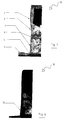
- Figure 1 shows a nonvolatile memory cell obtained by means of a sealing process according to the prior art;
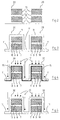
- Figures 2 - 5 show a sequence of a sealing process of the nonvolatile memory cell according to the present invention;
- Figure 6 shows a nonvolatile memory cell obtained by means of the sealing process according to the present invention.
-
- As Figure 1 shows, a sealing process of a cell implemented by means of a thermal re - oxidation acts in a different way on the various substrates, such as diversely doped silicon, polysilicon WSi2 etc., exposed to the oxidant agents.
- In fact in Figure 1, it is possible to note, that this selectivity of the sealing process, causes oxide thicknesses different from the distinct parts of the device.
- Particularly in Figure 1, a cross sectional view of a
nonvolatile memory 10 is shown, and it is possible to note that in afirst part 1, identifiable as a floating gate, and in asecond part 2, identifiable as an interpoly dielectric, the thickness of the oxide is about 100 - 300 Å. - Moreover it is possible to note that in a
third part 3, identifiable as a tunnel oxide, and in afourth part 4, identifiable as a control gate, the thickness of the oxide is about 200 - 500 Å. - Moreover a such sealing process causes some narrowing 5 and 6 where the active dielectrics are implemented, that is in proximity respectively of the
tunnel oxide 3 anddielectric interpoly 2. - On the contrary the new sealing process, implemented by an oxide densified by a Chemical Vapor Deposition (CVD), opportunely modified, produces an silicon oxide layer more uniform with respect to the prior art, as shown in the sequence of Figures 2 - 5.
- Wherever possible, the same reference numbers are used in the sequence of Figures 2 - 5 and the description to refer to the same or like parts.
- Particularly, in Figure 2, the first step of the innovative process is the definition of the nonvolatile memory cell, that is, there is the definition of a
tunnel oxide 7, of thefloating gate 8, of the interpoly dielectric 9 and of thecontrol gate 10. - At this step, control logic transistors can eventually be already defined too.
- Particularly, in Figure 3, the second step of the innovative process is the deposition of an
oxide layer 11 by means of CVD technique in batch o single wafer systems, made by at a temperature lower than 1000 °C. - The innovative process is completely defined by an eventual nitridation phase and an obligatory densification phase, as heretofore described.
- In fact, in Figure 4, the third step of the innovative process is the nitridation (depicted as a plurality of vertical arrows 12) of said deposed
silicon oxide layer 11 in batch or single wafer systems by means of NH3, N2O, NO gases or plasma assisted nitridation. - The nitridation phase involves the incorporation of nitrogen gas in all the possible interfaces such as SiO2 / Si or SiO2 / poly, as depicted in figure 4 with the
line 15. - By the way this third step can be an optional step of the inventive process.
- Particularly, in Figure 5, the fourth step of the innovative process is the densification (depicted as a plurality of vertical arrows 13) of said deposed
silicon oxide layer 11 in batch or single wafer systems by a next treatment, for example a thermal treatment in inert atmosphere, such as N2, or by a thermal treatment in oxidant atmosphere, such as H2O or O2. - Due to presence of the CVD oxide layer, the densification step can be executed by using low temperature process, such as 800 °C for some hours, or higher temperature treatment for shorter time.
- In this way the new sealing process, implemented by the
oxide 11 obtained by a CVD technique, forms a sealing of anonvolatile memory cell 30 with an overall lower thermal budget, and no exposure of the silicon surface at oxygen at a temperature higher than 800 °C. - Moreover the new sealing process forms a perfect sealing of the silicon surface of the
nonvolatile memory cell 30, as shown in the cross sectional view of Figure 6. - In Figure 6 the sealing process of a nonvolatile cell according to the present invention is shown, wherein it is to be noted the thickness uniformity of the
silicon oxide layer 11. - In fact the Applicant has found that the thickness of the
silicon oxide layer 11, deposed around the perimeter of saidnonvolatile memory cell 30, is about 100 - 300 Å. - Further it is possible to note that the narrowing 5 and 6 are completely deleted by the innovative sealing process.
Claims (11)
- Method for sealing a nonvolatile memory device, characterized in that to comprise the following steps of:a) defining a nonvolatile memory cell (20), being composed by the overlap of a tunnel oxide (3), of a floating gate (1), of an interpoly dielectric (2), and of a control gate (4);b) deposing a silicon oxide layer (11) by a CVD (Chemical Vapor Deposition) at a temperature lower than 1000 °C on said control gate (4);c) densifing said silicon oxide layer (11) by a further thermal treatment (13).
- Method for sealing a memory device according claim 1, characterized by the fact said step (c) is made by means of oxidant atmosphere treatment (13).
- Method for sealing a memory device according claim 1, characterized by the fact said step (c) is made by means of an inert atmosphere treatment (13).
- Method for sealing a memory device according claim 1, characterized by the fact to comprise further a step of nitridation (12) of said silicon oxide layer (11) by means of a NH3 gas.
- Method for sealing a memory device according claim 1, characterized by the fact that said step (b) is made at a temperature of about 800 °C.
- Method for sealing a memory device according claim 4, characterized by the fact that said step of nitridation (12) of said silicon oxide layer (11) is made by means of a N2O gas.
- Method for sealing a memory device according claim 4, characterized by the fact that said step of nitridation (12) of said silicon oxide layer (11) is made by means of a NO gas.
- Method for sealing a memory device according claim 4, characterized by the fact that said step of nitridation (12) of said silicon oxide layer (11) is made by means of plasma assisted nitridation.
- Method for sealing a memory device according claim 2, characterized by the fact said oxidant atmosphere treatment (13) is made by H2O gas.
- Method for sealing a memory device according claim 2, characterized by the fact said oxidant atmosphere treatment (13) is made by O2 gas.
- Method for sealing a memory device according claim 3, characterized by the fact said inert atmosphere treatment (13) is made by N2 gas.
Priority Applications (1)
| Application Number | Priority Date | Filing Date | Title |
|---|---|---|---|
| EP01830267A EP1253635A1 (en) | 2001-04-23 | 2001-04-23 | Method for sealing a memory device |
Applications Claiming Priority (1)
| Application Number | Priority Date | Filing Date | Title |
|---|---|---|---|
| EP01830267A EP1253635A1 (en) | 2001-04-23 | 2001-04-23 | Method for sealing a memory device |
Publications (1)
| Publication Number | Publication Date |
|---|---|
| EP1253635A1 true EP1253635A1 (en) | 2002-10-30 |
Family
ID=8184495
Family Applications (1)
| Application Number | Title | Priority Date | Filing Date |
|---|---|---|---|
| EP01830267A Withdrawn EP1253635A1 (en) | 2001-04-23 | 2001-04-23 | Method for sealing a memory device |
Country Status (1)
| Country | Link |
|---|---|
| EP (1) | EP1253635A1 (en) |
Citations (4)
| Publication number | Priority date | Publication date | Assignee | Title |
|---|---|---|---|---|
| US5208174A (en) * | 1990-07-05 | 1993-05-04 | Kabushiki Kaisha Toshiba | Method for manufacturing a nonvolatile semiconductor memory device |
| US5460992A (en) * | 1994-05-25 | 1995-10-24 | Nec Corporation | Fabricating non-volatile memory device having a multi-layered gate electrode |
| US5571736A (en) * | 1987-12-03 | 1996-11-05 | Texas Instruments Incorporated | Fabricating a high density EPROM cell by removing a portion of the field insulator regions |
| US6037223A (en) * | 1998-10-23 | 2000-03-14 | Taiwan Semiconductor Manufacturing Company, Ltd. | Stack gate flash memory cell featuring symmetric self aligned contact structures |
-
2001
- 2001-04-23 EP EP01830267A patent/EP1253635A1/en not_active Withdrawn
Patent Citations (4)
| Publication number | Priority date | Publication date | Assignee | Title |
|---|---|---|---|---|
| US5571736A (en) * | 1987-12-03 | 1996-11-05 | Texas Instruments Incorporated | Fabricating a high density EPROM cell by removing a portion of the field insulator regions |
| US5208174A (en) * | 1990-07-05 | 1993-05-04 | Kabushiki Kaisha Toshiba | Method for manufacturing a nonvolatile semiconductor memory device |
| US5460992A (en) * | 1994-05-25 | 1995-10-24 | Nec Corporation | Fabricating non-volatile memory device having a multi-layered gate electrode |
| US6037223A (en) * | 1998-10-23 | 2000-03-14 | Taiwan Semiconductor Manufacturing Company, Ltd. | Stack gate flash memory cell featuring symmetric self aligned contact structures |
Similar Documents
| Publication | Publication Date | Title |
|---|---|---|
| US6596576B2 (en) | Limiting hydrogen ion diffusion using multiple layers of SiO2 and Si3N4 | |
| US6734069B2 (en) | Method of forming a high dielectric constant insulating film and method of producing semiconductor device using the same | |
| US5861347A (en) | Method for forming a high voltage gate dielectric for use in integrated circuit | |
| US6140187A (en) | Process for forming metal oxide semiconductors including an in situ furnace gate stack with varying silicon nitride deposition rate | |
| KR100624290B1 (en) | Manufacturing Method of Flash Memory Device | |
| KR101414067B1 (en) | An electrode of semiconductor device and method of forming the same | |
| US6706613B2 (en) | Methods for manufacturing stacked gates including oxide/nitride/oxide (ONO) interlayer dielectrics using pre-annealing and/or post-annealing in nitrogen | |
| US7157339B2 (en) | Method for fabricating semiconductor devices having dual gate oxide layers | |
| KR20020002624A (en) | Method for forming gate electrode in semiconductor deivce | |
| US20070205446A1 (en) | Reducing nitrogen concentration with in-situ steam generation | |
| US6274429B1 (en) | Use of Si-rich oxide film as a chemical potential barrier for controlled oxidation | |
| KR100444604B1 (en) | Method of manufacturing a flash memory cell | |
| US20030119235A1 (en) | MOS semiconductor device having gate insulating film containing nitrogen and method of manufacturing the same | |
| US6207542B1 (en) | Method for establishing ultra-thin gate insulator using oxidized nitride film | |
| KR20040077969A (en) | Method of forming layers of oxide of different thicknesses on a surface of a substrate | |
| KR20060100092A (en) | Manufacturing Method of Semiconductor Device | |
| KR100666384B1 (en) | Semiconductor device having composite barrier film and method of manufacturing same | |
| US20050153503A1 (en) | Method of manufacturing flash memory device | |
| US6051510A (en) | Method of using a hard mask to grow dielectrics with varying characteristics | |
| JPH03257828A (en) | Manufacture of semiconductor device | |
| KR20080087282A (en) | Dual polygate formation method of semiconductor device | |
| EP0788168A1 (en) | Process of fabricating non-volatile floating-gate memory devices, and memory device fabricated thereby | |
| KR0171936B1 (en) | Method of manufacturing transistor in semiconductor device | |
| KR100997781B1 (en) | Manufacturing method of ypyrom element | |
| KR100207524B1 (en) | Process for fabricating semiconductor device |
Legal Events
| Date | Code | Title | Description |
|---|---|---|---|
| PUAI | Public reference made under article 153(3) epc to a published international application that has entered the european phase |
Free format text: ORIGINAL CODE: 0009012 |
|
| AK | Designated contracting states |
Kind code of ref document: A1 Designated state(s): AT BE CH CY DE DK ES FI FR GB GR IE IT LI LU MC NL PT SE TR |
|
| AX | Request for extension of the european patent |
Free format text: AL;LT;LV;MK;RO;SI |
|
| AKX | Designation fees paid | ||
| REG | Reference to a national code |
Ref country code: DE Ref legal event code: 8566 |
|
| STAA | Information on the status of an ep patent application or granted ep patent |
Free format text: STATUS: THE APPLICATION IS DEEMED TO BE WITHDRAWN |
|
| 18D | Application deemed to be withdrawn |
Effective date: 20030501 |