EP1253633A2 - Wafer holding device - Google Patents
Wafer holding device Download PDFInfo
- Publication number
- EP1253633A2 EP1253633A2 EP02008619A EP02008619A EP1253633A2 EP 1253633 A2 EP1253633 A2 EP 1253633A2 EP 02008619 A EP02008619 A EP 02008619A EP 02008619 A EP02008619 A EP 02008619A EP 1253633 A2 EP1253633 A2 EP 1253633A2
- Authority
- EP
- European Patent Office
- Prior art keywords
- wafer
- chuck
- seat
- lever
- holding device
- Prior art date
- Legal status (The legal status is an assumption and is not a legal conclusion. Google has not performed a legal analysis and makes no representation as to the accuracy of the status listed.)
- Granted
Links
Images






Classifications
-
- H—ELECTRICITY
- H10—SEMICONDUCTOR DEVICES; ELECTRIC SOLID-STATE DEVICES NOT OTHERWISE PROVIDED FOR
- H10P—GENERIC PROCESSES OR APPARATUS FOR THE MANUFACTURE OR TREATMENT OF DEVICES COVERED BY CLASS H10
- H10P72/00—Handling or holding of wafers, substrates or devices during manufacture or treatment thereof
- H10P72/70—Handling or holding of wafers, substrates or devices during manufacture or treatment thereof for supporting or gripping
- H10P72/76—Handling or holding of wafers, substrates or devices during manufacture or treatment thereof for supporting or gripping using mechanical means, e.g. clamps or pinches
- H10P72/7604—Handling or holding of wafers, substrates or devices during manufacture or treatment thereof for supporting or gripping using mechanical means, e.g. clamps or pinches the wafers being placed on a susceptor, stage or support
- H10P72/7608—Handling or holding of wafers, substrates or devices during manufacture or treatment thereof for supporting or gripping using mechanical means, e.g. clamps or pinches the wafers being placed on a susceptor, stage or support characterised by a plurality of separate clamping members, e.g. clamping fingers
-
- H—ELECTRICITY
- H10—SEMICONDUCTOR DEVICES; ELECTRIC SOLID-STATE DEVICES NOT OTHERWISE PROVIDED FOR
- H10P—GENERIC PROCESSES OR APPARATUS FOR THE MANUFACTURE OR TREATMENT OF DEVICES COVERED BY CLASS H10
- H10P72/00—Handling or holding of wafers, substrates or devices during manufacture or treatment thereof
- H10P72/06—Apparatus for monitoring, sorting, marking, testing or measuring
- H10P72/0616—Monitoring of warpages, curvatures, damages, defects or the like
-
- H—ELECTRICITY
- H10—SEMICONDUCTOR DEVICES; ELECTRIC SOLID-STATE DEVICES NOT OTHERWISE PROVIDED FOR
- H10P—GENERIC PROCESSES OR APPARATUS FOR THE MANUFACTURE OR TREATMENT OF DEVICES COVERED BY CLASS H10
- H10P72/00—Handling or holding of wafers, substrates or devices during manufacture or treatment thereof
- H10P72/70—Handling or holding of wafers, substrates or devices during manufacture or treatment thereof for supporting or gripping
- H10P72/74—Handling or holding of wafers, substrates or devices during manufacture or treatment thereof for supporting or gripping using temporarily an auxiliary support
-
- Y—GENERAL TAGGING OF NEW TECHNOLOGICAL DEVELOPMENTS; GENERAL TAGGING OF CROSS-SECTIONAL TECHNOLOGIES SPANNING OVER SEVERAL SECTIONS OF THE IPC; TECHNICAL SUBJECTS COVERED BY FORMER USPC CROSS-REFERENCE ART COLLECTIONS [XRACs] AND DIGESTS
- Y10—TECHNICAL SUBJECTS COVERED BY FORMER USPC
- Y10T—TECHNICAL SUBJECTS COVERED BY FORMER US CLASSIFICATION
- Y10T279/00—Chucks or sockets
- Y10T279/18—Pivoted jaw
Definitions
- the present invention relates to a wafer holding device in a surface inspection system to be used in an inspecting process for manufacture of semiconductor products.
- a semiconductor product is manufactured by forming a large number of semiconductor devices on a wafer. Because of the requirements on high density and high integration, increasingly finer fabrication is needed. Further, for the purpose of improving the production yield, a wafer with an increasingly larger diameter is now being produced.
- a surface inspection of the wafer is performed by using an inspection system, and attaching condition of the particles on the wafer and damage of the wafer are inspected.
- the wafer In the surface inspection for the wafer, the wafer is rotated at high speed. A laser beam is irradiated to the wafer surface and is scanned in a circumferential direction. The laser beam reflected from the wafer surface is received, and the attachment of the particles, etc. is detected by examining the reflecting condition.
- the wafer is now being produced with increasingly larger diameter. Further, there are demands to improve the throughput and to improve the productivity, and wafer rotating speed during the inspecting is also increased. Therefore, during the inspecting of the wafer, high centrifugal force is applied on the wafer held in the device.
- a wafer holding device must reliably hold the wafer even at high-speed rotation under high centrifugal force applied.
- a wafer chuck 1 is provided on an upper end of a rotation shaft (not shown).
- the wafer chuck 1 comprises a shaft 2 connected to the rotation shaft and a vacuum suction unit 3 in a disk-like shape.
- a number of circumferential grooves 4 are formed coaxially on an upper surface of the vacuum suction unit 3.
- a radial groove 5 is formed in a radial direction, and the circumferential grooves 4 are communicated with the radial groove 5.
- the shaft 2 is designed with a hollow portion 6, and it is communicated with a vacuum pumping equipment (not shown) via the hollow portion 6.
- the wafer 7 When the wafer 7 is chucked, the wafer 7 is received so that the wafer 7 is coaxially aligned on the vacuum suction unit 3.
- the wafer 7 has a diameter larger than the diameter of the vacuum suction unit 3, and the peripheral portion is protruded.
- each of the circumferential groove 4 and the radial groove 5 is turned to a closed space.
- the inner spaces of the circumferential groove 4 and the radial groove 5 are turned to negative pressure. By the pressure difference from outside, the wafer 7 is sucked and held by the vacuum suction unit 3.
- the convex portions 8 are brought into contact with an entire rear surface of the wafer 7, and high contact pressure is applied on the contact portion. This may lead to generation of damage and also to the possibility that foreign objects may be attached on the rear surface of the wafer 7.
- the wafer 7 may not be aligned with the center of the vacuum suction unit 3 due to angular acceleration at the initiation of rotation or at the stopping of the vacuum suction unit 3.
- the wafer 7 is rotated at high speed, high centrifugal force is applied on the wafer.
- the wafer 7 may be detached from the vacuum suction unit 3.
- the wafer holding device comprises a rotating baseplate, a wafer seat which is provided on the rotating baseplate coaxially with the rotating baseplate and which receives a peripheral edge of a wafer by a circumference, a predetermined number of chuck levers rotatably mounted on the wafer seat so that the chuck levers can be rotated around an axis extending in a tangential direction on a circumference of the rotating baseplate, and springs for resiliently pushing an end of the chuck lever toward the wafer seat, wherein the peripheral edge of the wafer received on the wafer seat is pinched by the wafer seat and the chuck lever.
- the present invention provides the wafer holding device as described above, wherein a wafer receiving surface of the wafer seat has a downslope gradient toward a center of the rotating baseplate, and a wafer abutting surface of the chuck lever has an upslope gradient toward the center. Further, the present invention provides the wafer holding device as described above, wherein the chuck lever is extended above and under the rotating baseplate, an outer end of a chuck shaft slidably provided in a radial direction is engaged with a lower end of the chuck lever, an inner end of the chuck shaft is engaged with a chuck disk provided coaxially with the rotating baseplate, the chuck shaft is displaced in the radial direction by rotation of the chuck disk, and the chuck lever is rotated.
- the present invention provides the wafer holding device as described above, wherein centrifugal force applied on a lower half of the chuck lever is designed to be bigger than centrifugal force applied on an upper half of the chuck lever. Further, the present invention provides the wafer holding device as described above, wherein the wafer seat has at least three notches, and there is provided a delivery pin which is positioned on each of the notches, which is movable in a vertical direction on the same circumference as the wafer seat, and which receives the wafer above the wafer seat.
- the present invention provides the wafer holding device as described above, wherein the device comprises a cylinder cam rotatably mounted with respect to the delivery pin, a chuck disk rotatably provided coaxially with the rotating baseplate, and a link bar for connecting the chuck disk with the cylinder cam, wherein the cylinder cam is rotated via the link bar by rotation of the chuck disk, and the delivery pin is moved up or down by rotation of the cylinder cam.
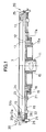
- Fig. 1 to Fig. 3 each represents an essential portion of a wafer holding device in the first embodiment.
- the left half of Fig. 1 shows the condition where a wafer is opened, and the right half shows the condition where the wafer is chucked.
- a rotating baseplate 12 in circular shape is fixed on a rotation shaft 11 of a motor, and a wafer seat 13 in a ring-like shape is fixed coaxially with the rotating baseplate 12 on an upper surface of the rotating baseplate 12.
- the wafer seat 13 has a diameter larger than a diameter of the wafer which is to be placed on the wafer seat 13, and the rotating baseplate 12 is designed in such manner that its peripheral portion is further extended and protruded by a predetermined extent from the wafer seat 13.
- a wafer receiving surface 13a and an escape surface 13b lower than the wafer receiving surface 13a are provided, and the wafer receiving surface 13a is designed in a conical curved surface with a downslope gradient toward the center.
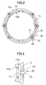
- notches 14 are formed at predetermined points (6 points except 2 points opposing to each other among 8 equally divided points of the circumference as shown in Fig. 2).
- Each of the notches 14 is formed in a rectangular groove from the upper surface of the wafer seat 13.
- the position of each of the notches 14 is on a radius of the rotating baseplate 12, and each pair of notches are at symmetrical positions with respect to the center of the rotating baseplate 12.
- a wafer clamper 20 (to be described later) is provided on the notch 14.
- a cam holder 15 coaxial with the rotating baseplate 12 is fixedly mounted on a rear surface of the rotating baseplate 12.
- the cam holder 15 is designed in a hollow shape so as to reduce an inertial force, and a flange 15a is formed on its lower end.
- a chuck disk 16 in a doughnut-like shape is rotatably mounted on the outer side of the cam holder 15, and the movement in an axial direction is restricted by the flange 15a and the rotating baseplate 12.
- the chuck disk 16 is reciprocally rotated at a predetermined angle by a chuck switching means (not shown).
- a cam groove 17 is formed from an upper surface. Thickness of an outer wall 17a of the cam grove 17 is changed in a circumferential direction within a predetermined range, and a recess 17b is formed. On the outer wall 17a, a cam follower 18 (to be described later) is rotatably abutted.
- a chuck shaft 19 is disposed on the lower side of the rotating baseplate 12, and an axis of the chuck shaft 19 runs in parallel to the radius of the rotating baseplate 12 where the notch 14 is provided.
- the chuck shaft 19 is slidably supported by bearing blocks 21 and 22.
- a guide hole 23 is formed on a lateral side of the bearing block 21, and a guide pin 24 studded on the chuck shaft 19 is slidably engaged in the guide hole 23.
- the cam follower 18 On one end of the chuck shaft 19 closer to the center, the cam follower 18 is rotatably mounted, and an outer end of the chuck shaft 19 is freely penetrating through a chuck lever 25 (to be described later). On a protruded end of the chuck lever 25, a washer 26 is mounted, and a pin 27 is further fixed, and the washer 26 is prevented from falling off by the pin 27.
- a compression spring 28 is positioned between the bearing block 22 and the chuck lever 25, and the spring resiliently pushes the chuck shaft 19 and the lower end of the chuck lever 25 in an outward direction. Therefore, the cam follower 18 is abutted on the outer wall 17a by a resilient force of the compression spring 28.
- a notch in a rectangular shape is formed to be in contact with the notch 14, and the chuck lever 25 is mounted on the notch via a holder 29.
- the chuck lever 25 is pivotally mounted on the holder 29 by a pin 31, which has an axis in a tangential direction on the circumference of the rotating baseplate 12, and the chuck lever 25 is removably engaged with the notch 14.
- the chuck lever 25, the holder 29 and the pin 31 make up together the wafer clamper 20.
- the lower half of the chuck lever 25 is extended in a downward direction from the rotating baseplate 12. Its upper half is extended in an upward direction from the rotating baseplate 12. It is designed in such manner that, when centrifugal force is applied on the upper half and the lower half of the chuck lever 25, the centrifugal force applied on the lower half is slightly bigger than the force applied on the upper half.
- the lower end of the chuck lever 25 is engaged with the chuck shaft 19.
- a wafer presser 25a in a beak-like shape and protruding toward the center is provided on the upper end of the chuck lever 25, a wafer presser 25a in a beak-like shape and protruding toward the center is provided on the upper end of the chuck lever 25, a wafer presser 25a in a beak-like shape and protruding toward the center is provided.
- the lower surface of the wafer presser 25a is designed as an inclined surface with an upslope gradient toward the center.
- Fig. 4 (A) and Fig. 5 (A) each represents a condition where the wafer is opened
- Fig. 4 (B) and Fig. 5 (B) each shows a condition where the chuck is closed.
- the chuck levers 25 are operated all synchronously.
- the chuck disk 16 When the chuck disk 16 is set to a wafer opening position, the thickness of the outer wall 17a reaches the maximum, and the chuck shaft 19 is pulled toward the center against the force of the compression spring 28. The lower end of the chuck lever 25 is rotated toward the center, and the wafer presser 25a is rotated and moved in the outward direction. As a result, it is completely separated from the wafer seat 13.
- the wafer 7 held by a robot hand (not shown) is placed on the wafer seat 13.
- An advancing direction of the robot hand is a direction toward the position where the notch 14 is not provided, and interference of the robot hand with the chuck lever 25 can be avoided.
- the thickness of the outer wall 17a is gradually decreased.
- the chuck shaft 19 is displaced in the outward direction by the resilient force of the compression spring 28.
- the wafer presser 25a is rotated toward the center, and a peripheral edge of the wafer 7 is pinched between the wafer seat 13 and the wafer presser 25a.
- the chuck shaft 19 and the chuck lever 25 are arranged in such manner that good balance is kept when the rotating baseplate 12 is rotated and no vibration occurs.
- the wafer is pinched by the inclined surface with the downslope gradient toward the center and by the inclined surface with the upslope gradient toward the center. Therefore, the wafer is constrained from movement in two directions, i.e. in a radial direction and a vertical direction in a single step. Because the wafer receiving surface 13a is in the downslope gradient toward the center, automatic aligning force is applied on the wafer 7 to be received on the wafer receiving surface 13a so that the wafer 7 is aligned with the center of the rotating baseplate 12.
- the upslope surface of the wafer presser 25a is brought into contact with the peripheral edge of the wafer 7, horizontal component force toward the center is generated as shown in Fig. 8. Also, an action is generated by this component force to align the wafer 7 with the center.
- the wafer 7 is decentered with respect to the wafer seat 13 when the wafer 7 is received. Even in such case, the chuck levers 25 are all synchronously operated when chucking by the chuck levers 25 is performed. Therefore, the wafer presser 25a on the decentered side first touches the wafer 7, and the wafer is moved toward the center. Further, when all of the wafer pressers 25a pinch the wafer 7, alignment with high accuracy can be achieved by the horizontal component force as described above.
- the force caused by angular acceleration is applied in the tangential direction of the circumference.
- the pin 31 of the chuck lever 25 is provided in the tangential direction. For this reason, even when the force caused by angular acceleration is applied, no force such as twisting is applied on the chuck lever 25, and the force applied on the chuck lever 25 is supported by the holder 29 via two side surfaces of the chuck lever 25. Accordingly, if backlash between the holder 29 and the chuck lever 25 is eliminated, no deviation of the wafer 7 occurs at the initiation of rotation and at the stopping.
- centrifugal force when centrifugal force is applied on the chuck lever 25 during rotation, it is designed in such manner that centrifugal force applied on the lower half of the chuck lever 25 is slightly bigger than centrifugal force applied on the upper half.
- a chucking force by the chuck lever 25 is increased. That is, the higher the rotating speed is, the more firmly the wafer is chucked, and the chucking is not loosened even when centrifugal force is increased.
- Fig. 10 shows flexed condition where the wafer 7 is received on the wafer seat 13 and is chucked.
- the wafer 7 is supported at the peripheral edge by the circumference, and it is smoothly bent or flexed toward the center by its own weight, and contour lines 9 of the flexion are in form of concentric circles.
- a laser beam is irradiated and scanned in a circumferential direction. If there is no irregular change in the circumferential direction, no trouble occurs in the inspection.
- the movement of the laser beam in the radial direction is far slower than rotation of the wafer 7. Thus, even when there may be displacement, it can be easily followed in the detection.
- the wafer seat 13 is designed as an integrated ring, while the wafer seat 13 may be designed in such manner that partial seats 32 in an arcuate shape may be arranged on the same circumference as shown in Fig. 11.
- the wafer seat 13 may be designed in such manner that the inertial force can be advantageously decreased.
- the partial seats 32 are provided at 8 points or more.
- the lower surface of the wafer receiving surface 13a and the wafer presser 25a are designed to have a linear cross-section, while it is needless to say that it may be designed to have a curved cross-section.
- the wafer clampers 20 are provided at 6 points of 8 equally divided points on the circumference. If we consider the condition such as distortion, it is preferable to chuck the wafer evenly on the circumference when the wafer is chucked.
- the wafer is chucked evenly on the circumference so that the moving of the wafer by the robot hand can be performed more smoothly.
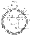
- the wafer seat 13 in a ring-like shape is provided on the upper surface of the rotating baseplate 12, and the wafer clampers 20 are arranged at each of 8 equally divided positions on the circumference of the wafer seat 13.
- a second notch 34 is disposed at each of 4 equally divided points on the circumference of the wafer seat 13 and the second notch 34 is deviated by 22.5° from the position of the notch 14.
- a wafer hoist 36 of a wafer lifting mechanism 35 is disposed on each of four of the second notches 34.
- a guide cylinder 37 is fixed on the second notch 34 of the rotating baseplate 12 from under the second notch so as to penetrate through it, and a delivery pin 38 is slidably engaged with the guide cylinder 37 so that the delivery pin can slide in a vertical direction.
- the upper end of the delivery pin 38 has an outer edge 38a and a wafer receiving surface 38b inclined with a downslope gradient from the outer edge 38a toward the center.
- a guide groove 39 is formed in a vertical direction on the guide cylinder 37, and a pin 41 slidably engaged with the guide groove 39 is erected on the delivery pin 38.
- the pin 41 and the guide groove 39 the delivery pin 38 is prevented from turning, and the delivery pin 38 can be moved up or down within the movable range of the pin 41.
- a cylinder cam 42 is rotatably engaged on a lower portion of the guide cylinder 37. As shown in Fig. 14, a cam groove 43 is formed on the cylinder cam 42.
- the cam groove 43 is provided with a predetermined gradient with respect to the generating line of the cylinder cam 42, and an upper end and a lower end of the cam groove are designed in a horizontal direction.
- the pin 41 is slidably engaged with the cam groove 43.
- a link strut 44 is erected, and the link strut 44 is disposed on a line which connects the center of the delivery pin 38 with the center of the rotation shaft 11.
- a link bar 45 is pivotally mounted on the link strut 44.
- An oblong hole 49 is formed on an outer end of the link bar 45, and another oblong hole 52 is formed on an inner end.
- a bracket 46 is fixed on the cylinder cam 42, and another bracket 47 is fixed on an outer peripheral surface of the chuck disk 16.
- a pin 48 is fixed on the bracket 46, and a pin 51 is fixed on the bracket 47.
- the pin 48 is slidably engaged in the oblong hole 49, and the outer end of the link bar 45 and the bracket 46 are connected via the pin 48.
- the pin 51 is slidably engaged in the oblong hole 52, and the inner end of the link bar 45 is connected with the bracket 47 via the pin 51.
- reference numeral 53 denotes a robot hand.
- Four of the delivery pins 38 are provided, while 3 delivery pins or 5 or more delivery pins may be provided so far as these can support the wafer.
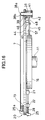
- the chuck lever 25 When the wafer 7 is received from the robot hand 53, the chuck lever 25 is erected, and the wafer presser 25a is separated from the wafer seat 13, and the delivery pin 38 is in a protruded and elevated position. (See Fig. 13.)
- the delivery pin 38 When the delivery pin 38 is protruded, the pin 41 is on the horizontal portion at the upper end of the cam groove 43, and the cylinder cam 42 is rotated clockwise as seen in Fig. 15.
- the wafer 7 is placed on the upper end of the delivery pin 38 by the robot hand 53, and the wafer 7 is supported by four delivery pins 38.
- the wafer 7 is positioned above the wafer seat 13 so that the robot hand 53 does not interfere with the chuck lever 25.
- the robot hand 53 is moved backward, and the chuck disk 16 is rotated at a predetermined angle in a counterclockwise direction in Fig. 15.
- the cylinder cam 42 is rotated via the link bar 45 in the counterclockwise direction in Fig.15.
- the pin 41 is moved downward along the cam groove 43, and the delivery pin 38 is moved down.
- the cam follower 18 is displaced synchronously to the outer side along the cam groove 17 (Fig. 5 (A) and Fig. 5 (B)).
- the chuck lever 25 chucks the wafer 7 by the force of the compression spring 28 (Fig. 16).
- the rotating baseplate 12 is rotated, and the surface inspection for the wafer 7 is performed.
- the wafer 7 is clamped evenly over the total circumference by the wafer clamper 20, and this prevents generation of the distortion.
- Fig. 17 shows an arrangement of the wafer seat 13 where the partial seats 32 in an arcuate shape are disposed on the same circumference instead of the wafer seat 13 designed in an integrated ring form. What is shown in Fig. 17 has the same meaning as the one shown in Fig. 11. By designing the seat in the partial seats 32, it is advantageous that an inertial force is decreased.
- a wafer holding device which comprises a rotating baseplate, a wafer seat which is provided on the rotating baseplate coaxially with the rotating baseplate and which receives a peripheral edge of a wafer by a circumference, a predetermined number of chuck levers rotatably mounted on the wafer seat so that the chuck levers can be rotated around an axis extending in a tangential direction on a circumference of the rotating baseplate, and springs for resiliently pushing an end of the chuck lever toward the wafer seat, wherein the peripheral edge of the wafer received on the wafer seat is pinched by the wafer seat and the chuck lever.
Landscapes
- Container, Conveyance, Adherence, Positioning, Of Wafer (AREA)
- Testing Or Measuring Of Semiconductors Or The Like (AREA)
Abstract
Description
- The present invention relates to a wafer holding device in a surface inspection system to be used in an inspecting process for manufacture of semiconductor products.
- A semiconductor product is manufactured by forming a large number of semiconductor devices on a wafer. Because of the requirements on high density and high integration, increasingly finer fabrication is needed. Further, for the purpose of improving the production yield, a wafer with an increasingly larger diameter is now being produced.
- With the progress of high density, high integration and finer production, particles attached on the wafer exert extensive influence on the product quality and the production yield. For this reason, the inspecting process is incorporated in the manufacturing process of semiconductor products. A surface inspection of the wafer is performed by using an inspection system, and attaching condition of the particles on the wafer and damage of the wafer are inspected.
- In the surface inspection for the wafer, the wafer is rotated at high speed. A laser beam is irradiated to the wafer surface and is scanned in a circumferential direction. The laser beam reflected from the wafer surface is received, and the attachment of the particles, etc. is detected by examining the reflecting condition.
- As described above, the wafer is now being produced with increasingly larger diameter. Further, there are demands to improve the throughput and to improve the productivity, and wafer rotating speed during the inspecting is also increased. Therefore, during the inspecting of the wafer, high centrifugal force is applied on the wafer held in the device.
- In this respect, a wafer holding device must reliably hold the wafer even at high-speed rotation under high centrifugal force applied.
- Description will be given below on a conventional type wafer holding device referring to Fig. 18 and Fig. 19.
- A
wafer chuck 1 is provided on an upper end of a rotation shaft (not shown). - The
wafer chuck 1 comprises ashaft 2 connected to the rotation shaft and avacuum suction unit 3 in a disk-like shape. A number of circumferential grooves 4 are formed coaxially on an upper surface of thevacuum suction unit 3. Aradial groove 5 is formed in a radial direction, and the circumferential grooves 4 are communicated with theradial groove 5. Theshaft 2 is designed with ahollow portion 6, and it is communicated with a vacuum pumping equipment (not shown) via thehollow portion 6. - When the
wafer 7 is chucked, thewafer 7 is received so that thewafer 7 is coaxially aligned on thevacuum suction unit 3. Thewafer 7 has a diameter larger than the diameter of thevacuum suction unit 3, and the peripheral portion is protruded. When thewafer 7 is received, each of the circumferential groove 4 and theradial groove 5 is turned to a closed space. By performing vacuum pumping through thehollow portion 6, the inner spaces of the circumferential groove 4 and theradial groove 5 are turned to negative pressure. By the pressure difference from outside, thewafer 7 is sucked and held by thevacuum suction unit 3. - However, in the conventional wafer holding device, as shown in Fig. 20, when the
wafer 7 is sucked by thevacuum suction unit 3, thewafer 7 is supported by convex portions 8 in arcuate shapes between the circumferential grooves 4, and the external pressure is applied on the entire surface of thewafer 7. As a result, delicate and complicated flexion occurs between the convex portions 8 and 8. Also, the portion protruding from thevacuum suction unit 3 is bent downward by its one weight. In case the flection is irregular, a direction of the laser beam reflected from the surface of thewafer 7 is changed irregularly. From the laser beam reflected from the normal surface, particles and surface abnormality are erroneously detected. This may cause erroneous measurement. - The convex portions 8 are brought into contact with an entire rear surface of the
wafer 7, and high contact pressure is applied on the contact portion. This may lead to generation of damage and also to the possibility that foreign objects may be attached on the rear surface of thewafer 7. - Also, close contact between the
wafer 7 and the convex portions 8 exerts strong influence on adsorption of thewafer 7. When foreign objects are attached on a contact surface of the convex portion 8, adsorption is decreased. As a result, thewafer 7 may not be aligned with the center of thevacuum suction unit 3 due to angular acceleration at the initiation of rotation or at the stopping of thevacuum suction unit 3. When thewafer 7 is rotated at high speed, high centrifugal force is applied on the wafer. When thewafer 7 is not aligned well with thevacuum suction unit 3 or the center of thewafer 7 is deviated at the time of attaching, thewafer 7 may be detached from thevacuum suction unit 3. - It is an object of the present invention to provide a wafer holding device, by which it is possible to reliably hold a wafer even during high-speed rotation and to prevent the development of complicated flexion on the surface of the wafer when the wafer is held in the device.
- To attain the above object, the wafer holding device according to the present invention comprises a rotating baseplate, a wafer seat which is provided on the rotating baseplate coaxially with the rotating baseplate and which receives a peripheral edge of a wafer by a circumference, a predetermined number of chuck levers rotatably mounted on the wafer seat so that the chuck levers can be rotated around an axis extending in a tangential direction on a circumference of the rotating baseplate, and springs for resiliently pushing an end of the chuck lever toward the wafer seat, wherein the peripheral edge of the wafer received on the wafer seat is pinched by the wafer seat and the chuck lever. Also, the present invention provides the wafer holding device as described above, wherein a wafer receiving surface of the wafer seat has a downslope gradient toward a center of the rotating baseplate, and a wafer abutting surface of the chuck lever has an upslope gradient toward the center. Further, the present invention provides the wafer holding device as described above, wherein the chuck lever is extended above and under the rotating baseplate, an outer end of a chuck shaft slidably provided in a radial direction is engaged with a lower end of the chuck lever, an inner end of the chuck shaft is engaged with a chuck disk provided coaxially with the rotating baseplate, the chuck shaft is displaced in the radial direction by rotation of the chuck disk, and the chuck lever is rotated. Also, the present invention provides the wafer holding device as described above, wherein centrifugal force applied on a lower half of the chuck lever is designed to be bigger than centrifugal force applied on an upper half of the chuck lever. Further, the present invention provides the wafer holding device as described above, wherein the wafer seat has at least three notches, and there is provided a delivery pin which is positioned on each of the notches, which is movable in a vertical direction on the same circumference as the wafer seat, and which receives the wafer above the wafer seat. Also, the present invention provides the wafer holding device as described above, wherein the device comprises a cylinder cam rotatably mounted with respect to the delivery pin, a chuck disk rotatably provided coaxially with the rotating baseplate, and a link bar for connecting the chuck disk with the cylinder cam, wherein the cylinder cam is rotated via the link bar by rotation of the chuck disk, and the delivery pin is moved up or down by rotation of the cylinder cam.
-
- Fig. 1
- is a sectional view seen from a front side of a first embodiment of the present invention;
- Fig. 2
- is a plan view of the first embodiment as given above;
- Fig. 3
- is a plan view of a part of a chuck lever in the first embodiment;
- Fig. 4
- (A) and Fig. 4 (B) each represents a front view for explanation showing operation of a wafer chuck;
- Fig. 5
- (A) and Fig. 5 (B) each represents a bottom view for explanation showing operation of the wafer chuck;
- Fig. 6
- is a front view of a part of the chuck lever in the first embodiment;
- Fig. 7
- is an enlarged view showing chucking condition of the wafer in the first embodiment;
- Fig. 8
- is an operational drawing showing a force of a wafer chuck in the first embodiment;
- Fig. 9
- is an operational drawing showing a force to be applied on a chucked portion of the wafer by rotation in the first embodiment;
- Fig. 10
- is a drawing to explain flexed condition of the wafer in the first embodiment;
- Fig. 11
- is a plan view showing another example of a wafer seat in the first embodiment;
- Fig. 12
- is a plan view showing a second embodiment of the present invention;
- Fig. 13
- is a front view of the second embodiment;
- Fig. 14
- is a partial side view showing the second embodiment;
- Fig. 15
- is a partial bottom view of the second embodiment;
- Fig. 16
- is a front view showing operation of the second embodiment;
- Fig. 17
- is a plan view showing another example of a wafer seat in the second embodiment;
- Fig. 18
- is a perspective view of a wafer chuck in a conventional example;
- Fig. 19
- is a sectional elevation view of the conventional example; and
- Fig. 20
- is a drawing to explain flexed condition of the wafer in the conventional example.
- Description will be given below on a first embodiment of the present invention referring to the drawings.
- Fig. 1 to Fig. 3 each represents an essential portion of a wafer holding device in the first embodiment. To facilitate the explanation, the left half of Fig. 1 shows the condition where a wafer is opened, and the right half shows the condition where the wafer is chucked.
- A rotating
baseplate 12 in circular shape is fixed on arotation shaft 11 of a motor, and awafer seat 13 in a ring-like shape is fixed coaxially with the rotatingbaseplate 12 on an upper surface of therotating baseplate 12. Thewafer seat 13 has a diameter larger than a diameter of the wafer which is to be placed on thewafer seat 13, and therotating baseplate 12 is designed in such manner that its peripheral portion is further extended and protruded by a predetermined extent from thewafer seat 13. - On an upper surface of the
wafer seat 13, a wafer receiving surface 13a and an escape surface 13b lower than the wafer receiving surface 13a are provided, and the wafer receiving surface 13a is designed in a conical curved surface with a downslope gradient toward the center. - On the
wafer seat 13,notches 14 are formed at predetermined points (6 points except 2 points opposing to each other among 8 equally divided points of the circumference as shown in Fig. 2). Each of thenotches 14 is formed in a rectangular groove from the upper surface of thewafer seat 13. The position of each of thenotches 14 is on a radius of therotating baseplate 12, and each pair of notches are at symmetrical positions with respect to the center of therotating baseplate 12. A wafer clamper 20 (to be described later) is provided on thenotch 14. - On a rear surface of the
rotating baseplate 12, acam holder 15 coaxial with the rotatingbaseplate 12 is fixedly mounted. Thecam holder 15 is designed in a hollow shape so as to reduce an inertial force, and aflange 15a is formed on its lower end. Achuck disk 16 in a doughnut-like shape is rotatably mounted on the outer side of thecam holder 15, and the movement in an axial direction is restricted by theflange 15a and therotating baseplate 12. Thechuck disk 16 is reciprocally rotated at a predetermined angle by a chuck switching means (not shown). - On the
chuck disk 16, acam groove 17 is formed from an upper surface. Thickness of anouter wall 17a of thecam grove 17 is changed in a circumferential direction within a predetermined range, and arecess 17b is formed. On theouter wall 17a, a cam follower 18 (to be described later) is rotatably abutted. - To match the position of each of the
notches 14, achuck shaft 19 is disposed on the lower side of therotating baseplate 12, and an axis of thechuck shaft 19 runs in parallel to the radius of therotating baseplate 12 where thenotch 14 is provided. Thechuck shaft 19 is slidably supported by bearingblocks guide hole 23 is formed on a lateral side of thebearing block 21, and aguide pin 24 studded on thechuck shaft 19 is slidably engaged in theguide hole 23. - On one end of the
chuck shaft 19 closer to the center, thecam follower 18 is rotatably mounted, and an outer end of thechuck shaft 19 is freely penetrating through a chuck lever 25 (to be described later). On a protruded end of thechuck lever 25, awasher 26 is mounted, and apin 27 is further fixed, and thewasher 26 is prevented from falling off by thepin 27. Acompression spring 28 is positioned between the bearingblock 22 and thechuck lever 25, and the spring resiliently pushes thechuck shaft 19 and the lower end of thechuck lever 25 in an outward direction. Therefore, thecam follower 18 is abutted on theouter wall 17a by a resilient force of thecompression spring 28. - On an outer edge of the
rotating baseplate 12, a notch in a rectangular shape is formed to be in contact with thenotch 14, and thechuck lever 25 is mounted on the notch via aholder 29. Thechuck lever 25 is pivotally mounted on theholder 29 by apin 31, which has an axis in a tangential direction on the circumference of therotating baseplate 12, and thechuck lever 25 is removably engaged with thenotch 14. Thechuck lever 25, theholder 29 and thepin 31 make up together thewafer clamper 20. - The lower half of the
chuck lever 25 is extended in a downward direction from the rotatingbaseplate 12. Its upper half is extended in an upward direction from the rotatingbaseplate 12. It is designed in such manner that, when centrifugal force is applied on the upper half and the lower half of thechuck lever 25, the centrifugal force applied on the lower half is slightly bigger than the force applied on the upper half. - As described above, the lower end of the
chuck lever 25 is engaged with thechuck shaft 19. On the upper end of thechuck lever 25, awafer presser 25a in a beak-like shape and protruding toward the center is provided. The lower surface of thewafer presser 25a is designed as an inclined surface with an upslope gradient toward the center. - Now, description will be given on operation of the wafer chuck referring to Fig. 4 to Fig. 9.
- Fig. 4 (A) and Fig. 5 (A) each represents a condition where the wafer is opened, and Fig. 4 (B) and Fig. 5 (B) each shows a condition where the chuck is closed.
- The chuck levers 25 are operated all synchronously.
- When the
chuck disk 16 is set to a wafer opening position, the thickness of theouter wall 17a reaches the maximum, and thechuck shaft 19 is pulled toward the center against the force of thecompression spring 28. The lower end of thechuck lever 25 is rotated toward the center, and thewafer presser 25a is rotated and moved in the outward direction. As a result, it is completely separated from thewafer seat 13. - The
wafer 7 held by a robot hand (not shown) is placed on thewafer seat 13. An advancing direction of the robot hand is a direction toward the position where thenotch 14 is not provided, and interference of the robot hand with thechuck lever 25 can be avoided. - When the
chuck disk 16 is rotated in a wafer chuck direction, the thickness of theouter wall 17a is gradually decreased. Thechuck shaft 19 is displaced in the outward direction by the resilient force of thecompression spring 28. Thewafer presser 25a is rotated toward the center, and a peripheral edge of thewafer 7 is pinched between thewafer seat 13 and thewafer presser 25a. - Under the condition where the
wafer 7 is pinched, thepin 27 is separated from thewasher 26, and a pressing force of thechuck lever 25 on thewafer 7 is determined by the resilient force of thecompression spring 28. - It is needless to say that the
chuck shaft 19 and thechuck lever 25 are arranged in such manner that good balance is kept when the rotatingbaseplate 12 is rotated and no vibration occurs. - Description will be given now on the pinched condition referring to Fig. 6, Fig. 7 and Fig. 8.
- As described above, the wafer is pinched by the inclined surface with the downslope gradient toward the center and by the inclined surface with the upslope gradient toward the center. Therefore, the wafer is constrained from movement in two directions, i.e. in a radial direction and a vertical direction in a single step. Because the wafer receiving surface 13a is in the downslope gradient toward the center, automatic aligning force is applied on the
wafer 7 to be received on the wafer receiving surface 13a so that thewafer 7 is aligned with the center of therotating baseplate 12. When the upslope surface of thewafer presser 25a is brought into contact with the peripheral edge of thewafer 7, horizontal component force toward the center is generated as shown in Fig. 8. Also, an action is generated by this component force to align thewafer 7 with the center. - It is supposed that the
wafer 7 is decentered with respect to thewafer seat 13 when thewafer 7 is received. Even in such case, the chuck levers 25 are all synchronously operated when chucking by the chuck levers 25 is performed. Therefore, thewafer presser 25a on the decentered side first touches thewafer 7, and the wafer is moved toward the center. Further, when all of thewafer pressers 25a pinch thewafer 7, alignment with high accuracy can be achieved by the horizontal component force as described above. - Next, when the rotating
baseplate 12 is rotated, a force caused by angular acceleration is applied on the wafer holding device as shown in Fig. 9 at the initiation of rotation and at the stopping. During rotation, centrifugal force is applied. - At the initiation of rotation and at the stopping, the force caused by angular acceleration is applied in the tangential direction of the circumference. The
pin 31 of thechuck lever 25 is provided in the tangential direction. For this reason, even when the force caused by angular acceleration is applied, no force such as twisting is applied on thechuck lever 25, and the force applied on thechuck lever 25 is supported by theholder 29 via two side surfaces of thechuck lever 25. Accordingly, if backlash between theholder 29 and thechuck lever 25 is eliminated, no deviation of thewafer 7 occurs at the initiation of rotation and at the stopping. - Next, when centrifugal force is applied on the
chuck lever 25 during rotation, it is designed in such manner that centrifugal force applied on the lower half of thechuck lever 25 is slightly bigger than centrifugal force applied on the upper half. With increase of the rotating speed, a chucking force by thechuck lever 25 is increased. That is, the higher the rotating speed is, the more firmly the wafer is chucked, and the chucking is not loosened even when centrifugal force is increased. - When the wafer is chucked, there is play as large as a gap between the
pin 27 and thewasher 26 on thechuck shaft 19. Centrifugal force is also applied on thechuck shaft 19, and stabilization is reached with thecam follower 18 is abutted on theouter wall 17a. - Fig. 10 shows flexed condition where the
wafer 7 is received on thewafer seat 13 and is chucked. Thewafer 7 is supported at the peripheral edge by the circumference, and it is smoothly bent or flexed toward the center by its own weight, andcontour lines 9 of the flexion are in form of concentric circles. - In the surface inspection of the
wafer 7, a laser beam is irradiated and scanned in a circumferential direction. If there is no irregular change in the circumferential direction, no trouble occurs in the inspection. The movement of the laser beam in the radial direction is far slower than rotation of thewafer 7. Thus, even when there may be displacement, it can be easily followed in the detection. - In the above first embodiment, the
wafer seat 13 is designed as an integrated ring, while thewafer seat 13 may be designed in such manner thatpartial seats 32 in an arcuate shape may be arranged on the same circumference as shown in Fig. 11. By providing thepartial seats 32, thewafer seat 13 may be designed in such manner that the inertial force can be advantageously decreased. - If we consider the flexion when the
wafer 7 is received, it is preferable that thepartial seats 32 are provided at 8 points or more. - In the first embodiment as described above, the lower surface of the wafer receiving surface 13a and the
wafer presser 25a are designed to have a linear cross-section, while it is needless to say that it may be designed to have a curved cross-section. - In the first embodiment as described above, consideration is given on the placement of the wafer by the robot hand, and the
wafer clampers 20 are provided at 6 points of 8 equally divided points on the circumference. If we consider the condition such as distortion, it is preferable to chuck the wafer evenly on the circumference when the wafer is chucked. - In the second embodiment as described below, the wafer is chucked evenly on the circumference so that the moving of the wafer by the robot hand can be performed more smoothly.
- In Fig. 12 to Fig. 16 showing the second embodiment, the same component as shown in Fig. 1 to Fig. 9 is referred by the same symbol, and detailed description is not given here.
- The
wafer seat 13 in a ring-like shape is provided on the upper surface of therotating baseplate 12, and thewafer clampers 20 are arranged at each of 8 equally divided positions on the circumference of thewafer seat 13. Asecond notch 34 is disposed at each of 4 equally divided points on the circumference of thewafer seat 13 and thesecond notch 34 is deviated by 22.5° from the position of thenotch 14. On each of four of thesecond notches 34, a wafer hoist 36 of awafer lifting mechanism 35 is disposed. - In the following, description will be given on the wafer hoist 36.
- A
guide cylinder 37 is fixed on thesecond notch 34 of therotating baseplate 12 from under the second notch so as to penetrate through it, and adelivery pin 38 is slidably engaged with theguide cylinder 37 so that the delivery pin can slide in a vertical direction. The upper end of thedelivery pin 38 has anouter edge 38a and awafer receiving surface 38b inclined with a downslope gradient from theouter edge 38a toward the center. - A
guide groove 39 is formed in a vertical direction on theguide cylinder 37, and apin 41 slidably engaged with theguide groove 39 is erected on thedelivery pin 38. By thepin 41 and theguide groove 39, thedelivery pin 38 is prevented from turning, and thedelivery pin 38 can be moved up or down within the movable range of thepin 41. - A
cylinder cam 42 is rotatably engaged on a lower portion of theguide cylinder 37. As shown in Fig. 14, acam groove 43 is formed on thecylinder cam 42. Thecam groove 43 is provided with a predetermined gradient with respect to the generating line of thecylinder cam 42, and an upper end and a lower end of the cam groove are designed in a horizontal direction. Thepin 41 is slidably engaged with thecam groove 43. - On the lower surface of the
rotating baseplate 12, alink strut 44 is erected, and thelink strut 44 is disposed on a line which connects the center of thedelivery pin 38 with the center of therotation shaft 11. Alink bar 45 is pivotally mounted on thelink strut 44. Anoblong hole 49 is formed on an outer end of thelink bar 45, and anotheroblong hole 52 is formed on an inner end. - A
bracket 46 is fixed on thecylinder cam 42, and anotherbracket 47 is fixed on an outer peripheral surface of thechuck disk 16. Apin 48 is fixed on thebracket 46, and apin 51 is fixed on thebracket 47. - The
pin 48 is slidably engaged in theoblong hole 49, and the outer end of thelink bar 45 and thebracket 46 are connected via thepin 48. Thepin 51 is slidably engaged in theoblong hole 52, and the inner end of thelink bar 45 is connected with thebracket 47 via thepin 51. - In Fig. 12,
reference numeral 53 denotes a robot hand. Four of the delivery pins 38 are provided, while 3 delivery pins or 5 or more delivery pins may be provided so far as these can support the wafer. - Now, description will be given on the delivery of the wafer in the second embodiment.
- When the
wafer 7 is received from therobot hand 53, thechuck lever 25 is erected, and thewafer presser 25a is separated from thewafer seat 13, and thedelivery pin 38 is in a protruded and elevated position. (See Fig. 13.) When thedelivery pin 38 is protruded, thepin 41 is on the horizontal portion at the upper end of thecam groove 43, and thecylinder cam 42 is rotated clockwise as seen in Fig. 15. - The
wafer 7 is placed on the upper end of thedelivery pin 38 by therobot hand 53, and thewafer 7 is supported by four delivery pins 38. Thewafer 7 is positioned above thewafer seat 13 so that therobot hand 53 does not interfere with thechuck lever 25. - The
robot hand 53 is moved backward, and thechuck disk 16 is rotated at a predetermined angle in a counterclockwise direction in Fig. 15. By the rotation of thechuck disk 16, thecylinder cam 42 is rotated via thelink bar 45 in the counterclockwise direction in Fig.15. By the rotation of thecylinder cam 42, thepin 41 is moved downward along thecam groove 43, and thedelivery pin 38 is moved down. When thedelivery pin 38 is moved down and thewafer 7 is placed on thewafer seat 13, thecam follower 18 is displaced synchronously to the outer side along the cam groove 17 (Fig. 5 (A) and Fig. 5 (B)). Thechuck lever 25 chucks thewafer 7 by the force of the compression spring 28 (Fig. 16). - The rotating
baseplate 12 is rotated, and the surface inspection for thewafer 7 is performed. - When the
wafer 7 is moved out after the inspection, the above procedure is reversed. - As described above, in the second embodiment, the
wafer 7 is clamped evenly over the total circumference by thewafer clamper 20, and this prevents generation of the distortion. - Fig. 17 shows an arrangement of the
wafer seat 13 where thepartial seats 32 in an arcuate shape are disposed on the same circumference instead of thewafer seat 13 designed in an integrated ring form. What is shown in Fig. 17 has the same meaning as the one shown in Fig. 11. By designing the seat in thepartial seats 32, it is advantageous that an inertial force is decreased. - According to the present invention, a wafer holding device is provided, which comprises a rotating baseplate, a wafer seat which is provided on the rotating baseplate coaxially with the rotating baseplate and which receives a peripheral edge of a wafer by a circumference, a predetermined number of chuck levers rotatably mounted on the wafer seat so that the chuck levers can be rotated around an axis extending in a tangential direction on a circumference of the rotating baseplate, and springs for resiliently pushing an end of the chuck lever toward the wafer seat, wherein the peripheral edge of the wafer received on the wafer seat is pinched by the wafer seat and the chuck lever. As a result, irregular deformation does not develop on the wafer received on the wafer seat, and the wafer can be reliably held even at the time of sudden rotation, stopping or during high-speed rotation. The edge of the wafer can be pinched without touching the front or rear surface of the wafer, and it is possible to prevent attachment of foreign objects or to avoid damage on the front and rear surfaces of the wafer.
Claims (6)
- A wafer holding device, comprising a rotating baseplate, a wafer seat which is provided on said rotating baseplate coaxially with said rotating baseplate and which receives a peripheral edge of a wafer by a circumference, a predetermined number of chuck levers rotatably mounted on said wafer seat so that said chuck levers can be rotated around an axis extending in a tangential direction on a circumference of said rotating baseplate, and springs for resiliently pushing an end of said chuck lever toward said wafer seat, wherein said peripheral edge of the wafer received on said wafer seat is pinched by said wafer seat and said chuck lever.
- A wafer holding device according to claim 1, wherein a wafer receiving surface of said wafer seat has a downslope gradient toward a center of the rotating baseplate, and a wafer abutting surface of said chuck lever has an upslope gradient toward said center.
- A wafer holding device according to claim 1, wherein said chuck lever is extended above and under said rotating baseplate, an outer end of a chuck shaft slidably provided in a radial direction is engaged with a lower end of said chuck lever, an inner end of the chuck shaft is engaged with a chuck disk provided coaxially with said rotating baseplate, the chuck shaft is displaced in the radial direction by rotation of the chuck disk, and said chuck lever is rotated.
- A wafer holding device according to claim 1, wherein centrifugal force applied on a lower half of said chuck lever is designed to be bigger than centrifugal force applied on an upper half of said chuck lever.
- A wafer holding device according to claim 1, wherein said wafer seat has at least three notches, and there is provided a delivery pin which is positioned on each of the notches, which is movable in a vertical direction on the same circumference as said wafer seat, and which receives the wafer above said wafer seat.
- A wafer holding device according to claim 5, wherein said device comprises a cylinder cam rotatably mounted with respect to said delivery pin, a chuck disk rotatably provided coaxially with said rotating baseplate, and a link bar for connecting said chuck disk with said cylinder cam, wherein said cylinder cam is rotated via said link bar by rotation of said chuck disk, and said delivery pin is moved up or down by rotation of the cylinder cam.
Applications Claiming Priority (2)
| Application Number | Priority Date | Filing Date | Title |
|---|---|---|---|
| JP2001125137A JP4488646B2 (en) | 2001-04-23 | 2001-04-23 | Wafer holding device |
| JP2001125137 | 2001-04-23 |
Publications (3)
| Publication Number | Publication Date |
|---|---|
| EP1253633A2 true EP1253633A2 (en) | 2002-10-30 |
| EP1253633A3 EP1253633A3 (en) | 2005-03-16 |
| EP1253633B1 EP1253633B1 (en) | 2010-11-17 |
Family
ID=18974410
Family Applications (1)
| Application Number | Title | Priority Date | Filing Date |
|---|---|---|---|
| EP02008619A Expired - Lifetime EP1253633B1 (en) | 2001-04-23 | 2002-04-17 | Wafer holding device |
Country Status (4)
| Country | Link |
|---|---|
| US (1) | US6761362B2 (en) |
| EP (1) | EP1253633B1 (en) |
| JP (1) | JP4488646B2 (en) |
| DE (1) | DE60238291D1 (en) |
Cited By (5)
| Publication number | Priority date | Publication date | Assignee | Title |
|---|---|---|---|---|
| EP1868238A2 (en) | 2006-06-14 | 2007-12-19 | Siemens Aktiengesellschaft | Clamping device for a wafer |
| DE102017128380A1 (en) * | 2017-10-30 | 2019-05-02 | Taiwan Semiconductor Manufacturing Co., Ltd. | Substrate vapor drying apparatus and method |
| US12020974B2 (en) | 2019-03-13 | 2024-06-25 | Core Flow Ltd. | Circular wafer lateral positioning device |
| EP4475170A1 (en) * | 2023-06-06 | 2024-12-11 | Siltronic AG | Holding device for a horizontally placed wafer of semiconductor material |
| EP4531084A1 (en) * | 2023-09-29 | 2025-04-02 | Bühler Alzenau GmbH | Support assembly and system |
Families Citing this family (50)
| Publication number | Priority date | Publication date | Assignee | Title |
|---|---|---|---|---|
| US6752442B2 (en) * | 2001-11-09 | 2004-06-22 | Speedfam-Ipec Corporation | Workpiece handling end-effector and a method for processing workpieces using a workpiece handling end-effector |
| US7032287B1 (en) * | 2002-07-19 | 2006-04-25 | Nanometrics Incorporated | Edge grip chuck |
| US7018555B2 (en) * | 2002-07-26 | 2006-03-28 | Dainippon Screen Mfg. Co., Ltd. | Substrate treatment method and substrate treatment apparatus |
| US7289198B2 (en) * | 2003-01-07 | 2007-10-30 | Intel Corporation | Process compensation for step and scan lithography |
| US6935638B2 (en) | 2003-02-21 | 2005-08-30 | Blue29, Llc | Universal substrate holder for treating objects in fluids |
| US7226055B1 (en) * | 2003-05-30 | 2007-06-05 | Lam Research Corporation | Substrate holding and spinning assembly and methods for making the same |
| US6860944B2 (en) * | 2003-06-16 | 2005-03-01 | Blue29 Llc | Microelectronic fabrication system components and method for processing a wafer using such components |
| DE102004036435B4 (en) * | 2003-08-07 | 2007-08-30 | Nanophotonics Ag | Holding device for disc-shaped objects |
| JP2005333063A (en) * | 2004-05-21 | 2005-12-02 | Renesas Technology Corp | Clamp member, film forming apparatus, film forming method, and semiconductor device manufacturing method |
| US7703823B2 (en) * | 2004-07-12 | 2010-04-27 | Rudolph Technologies, Inc. | Wafer holding mechanism |
| JP4763338B2 (en) * | 2005-05-09 | 2011-08-31 | タツモ株式会社 | Board gripping mechanism |
| US20070145231A1 (en) * | 2005-12-21 | 2007-06-28 | Chunghwa Picture Tubes, Ltd | Substrate buffer clamp |
| CN1986874A (en) * | 2005-12-23 | 2007-06-27 | 鸿富锦精密工业(深圳)有限公司 | Anode plate and its sputtering apparatus including it |
| US20070215049A1 (en) * | 2006-03-14 | 2007-09-20 | Applied Materials, Inc. | Transfer of wafers with edge grip |
| JP4814731B2 (en) | 2006-08-30 | 2011-11-16 | 株式会社日立ハイテクノロジーズ | Substrate holding apparatus, inspection or processing apparatus, substrate holding method, inspection or processing method, and inspection apparatus |
| WO2008072694A1 (en) * | 2006-12-14 | 2008-06-19 | Is Technology Japan, Inc. | Disc holding apparatus and defect/foreign material detecting apparatus |
| US8042254B1 (en) * | 2006-12-22 | 2011-10-25 | Kla-Tencor Corporation | Method for improving edge handling chuck aerodynamics |
| TWI538094B (en) * | 2009-03-31 | 2016-06-11 | 蘭研究公司 | Device for processing disc-shaped articles |
| CN101656223B (en) * | 2009-07-29 | 2011-11-02 | 东莞宏威数码机械有限公司 | Multi-gripper repetitive intelligent grabbing and releasing device |
| KR101084268B1 (en) * | 2009-09-25 | 2011-11-16 | 삼성모바일디스플레이주식회사 | Substrate centering device and organic material deposition system having same |
| US9130002B2 (en) | 2010-05-07 | 2015-09-08 | Lam Research Ag | Device for holding wafer shaped articles |
| US9218990B2 (en) * | 2011-10-07 | 2015-12-22 | Varian Semiconductor Equipment Associates, Inc. | Method and apparatus for holding a plurality of substrates for processing |
| CN102569150B (en) * | 2012-02-23 | 2014-12-10 | 北京七星华创电子股份有限公司 | Device and method for clamping easily cleaned thin-walled disc |
| JP6018404B2 (en) * | 2012-04-25 | 2016-11-02 | 株式会社荏原製作所 | Substrate processing equipment |
| CN102945820B (en) * | 2012-10-23 | 2015-03-18 | 北京七星华创电子股份有限公司 | Disk holding device |
| US9589818B2 (en) * | 2012-12-20 | 2017-03-07 | Lam Research Ag | Apparatus for liquid treatment of wafer shaped articles and liquid control ring for use in same |
| JP6057334B2 (en) * | 2013-03-15 | 2017-01-11 | 株式会社Screenホールディングス | Substrate processing equipment |
| US20140293291A1 (en) * | 2013-04-01 | 2014-10-02 | Kla-Tencor Corporation | Wafer Shape and Thickness Measurement System Utilizing Shearing Interferometers |
| JP6255650B2 (en) * | 2013-05-13 | 2018-01-10 | 株式会社Screenホールディングス | Substrate processing equipment |
| JP6179012B2 (en) * | 2013-07-28 | 2017-08-16 | アテル株式会社 | Wafer positioning device |
| US9653338B2 (en) * | 2013-12-23 | 2017-05-16 | Kla-Tencor Corporation | System and method for non-contact wafer chucking |
| DE102014119365B4 (en) * | 2014-12-22 | 2023-01-26 | VON ARDENNE Asset GmbH & Co. KG | Substrate holding device, method for equipping a substrate holding device and method for producing a substrate holding device |
| JP6456712B2 (en) * | 2015-02-16 | 2019-01-23 | 東京エレクトロン株式会社 | Substrate holding mechanism and substrate processing apparatus using the same |
| US9966292B2 (en) * | 2016-07-12 | 2018-05-08 | Globalfoundries Inc. | Centering fixture for electrostatic chuck system |
| US10083852B1 (en) * | 2017-05-12 | 2018-09-25 | Kla-Tencor Corporation | Floating wafer chuck |
| JP6948860B2 (en) * | 2017-07-14 | 2021-10-13 | 株式会社荏原製作所 | Board holding device |
| TWI766105B (en) * | 2017-09-28 | 2022-06-01 | 美商魯道夫科技股份有限公司 | Wafer-level package assembly handling |
| JP6946151B2 (en) * | 2017-11-13 | 2021-10-06 | 株式会社荏原製作所 | A board processing device including a board holding device and a board holding device |
| US10658221B2 (en) | 2017-11-14 | 2020-05-19 | Taiwan Semiconductor Manufacturing Co., Ltd. | Semiconductor wafer cleaning apparatus and method for cleaning semiconductor wafer |
| US10811299B2 (en) * | 2018-05-04 | 2020-10-20 | Lam Research Corporation | Wafer chuck assembly |
| US11037809B2 (en) * | 2019-07-17 | 2021-06-15 | Taiwan Semiconductor Manufacturing Co., Ltd. | Transfer device and method for transferring substrate without unexpected rotation |
| US11217474B2 (en) * | 2019-12-06 | 2022-01-04 | Government Of The United States Of America, As Represented By The Secretary Of Commerce | Non-vacuum, non-contact spinner wafer chuck |
| TWI748560B (en) * | 2020-07-15 | 2021-12-01 | 弘塑科技股份有限公司 | Automatic wafer positioning assembly |
| CN113948437B (en) * | 2020-07-15 | 2024-11-05 | 弘塑科技股份有限公司 | Automatic wafer positioning assembly |
| CN112736014B (en) * | 2020-12-30 | 2024-01-16 | 中科晶源微电子技术(北京)有限公司 | Wafer locking mechanism, wafer positioning device and wafer transport equipment for locking wafers |
| DE102021109210B4 (en) * | 2021-04-13 | 2024-07-25 | Pva Tepla Analytical Systems Gmbh | Wafer chuck for handling and transmitting a wafer in an acoustic scanning microscope, use of a wafer chuck and wafer processing device with a wafer chuck |
| KR102637363B1 (en) * | 2021-12-30 | 2024-02-15 | 주식회사 에이이엘코리아 | Clamping apparatus for single type cleaning apparatus for substrate fixing |
| US20240376591A1 (en) * | 2023-05-08 | 2024-11-14 | Applied Materials, Inc. | Adjustable clamp for physical vapor deposition |
| CN117080155B (en) * | 2023-10-13 | 2024-04-09 | 无锡星微科技有限公司 | Multi-degree-of-freedom mobile device for wafer inspection |
| CN118501196B (en) * | 2024-04-11 | 2025-05-23 | 深圳市埃芯半导体科技有限公司 | Positioning chuck and semiconductor wafer analysis device |
Citations (5)
| Publication number | Priority date | Publication date | Assignee | Title |
|---|---|---|---|---|
| US5040484A (en) | 1987-05-04 | 1991-08-20 | Varian Associates, Inc. | Apparatus for retaining wafers |
| US5775000A (en) | 1996-05-13 | 1998-07-07 | Ebara Corporation | Substrate gripper device for spin drying |
| US5954072A (en) | 1997-01-24 | 1999-09-21 | Tokyo Electron Limited | Rotary processing apparatus |
| US6167893B1 (en) | 1999-02-09 | 2001-01-02 | Novellus Systems, Inc. | Dynamic chuck for semiconductor wafer or other substrate |
| US6217034B1 (en) | 1998-09-24 | 2001-04-17 | Kla-Tencor Corporation | Edge handling wafer chuck |
Family Cites Families (11)
| Publication number | Priority date | Publication date | Assignee | Title |
|---|---|---|---|---|
| JPH03128943U (en) * | 1990-04-09 | 1991-12-25 | ||
| JPH0735395Y2 (en) * | 1990-09-27 | 1995-08-09 | 株式会社エンヤシステム | Spin chuck |
| JPH06196543A (en) * | 1992-12-24 | 1994-07-15 | Sumitomo Metal Ind Ltd | Sample transport device |
| JP2862754B2 (en) * | 1993-04-19 | 1999-03-03 | 東京エレクトロン株式会社 | Processing device and rotating member |
| JPH10335287A (en) * | 1997-06-05 | 1998-12-18 | Toshiba Corp | Substrate processing equipment |
| JPH1167880A (en) * | 1997-08-18 | 1999-03-09 | Toshiba Mach Co Ltd | Wafer rotating chuck |
| US5974681A (en) * | 1997-09-10 | 1999-11-02 | Speedfam-Ipec Corp. | Apparatus for spin drying a workpiece |
| JPH1197515A (en) * | 1997-09-22 | 1999-04-09 | Toshiba Corp | Rotary table for wafer support |
| JPH11283957A (en) * | 1998-03-31 | 1999-10-15 | Kaijo Corp | Single wafer spin dryer for semiconductor wafers |
| JP2000332085A (en) * | 1999-05-19 | 2000-11-30 | Sony Corp | Wafer clamping device |
| US6578853B1 (en) * | 2000-12-22 | 2003-06-17 | Lam Research Corporation | Chuck assembly for use in a spin, rinse, and dry module and methods for making and implementing the same |
-
2001
- 2001-04-23 JP JP2001125137A patent/JP4488646B2/en not_active Expired - Fee Related
-
2002
- 2002-04-12 US US10/121,230 patent/US6761362B2/en not_active Expired - Fee Related
- 2002-04-17 DE DE60238291T patent/DE60238291D1/en not_active Expired - Lifetime
- 2002-04-17 EP EP02008619A patent/EP1253633B1/en not_active Expired - Lifetime
Patent Citations (5)
| Publication number | Priority date | Publication date | Assignee | Title |
|---|---|---|---|---|
| US5040484A (en) | 1987-05-04 | 1991-08-20 | Varian Associates, Inc. | Apparatus for retaining wafers |
| US5775000A (en) | 1996-05-13 | 1998-07-07 | Ebara Corporation | Substrate gripper device for spin drying |
| US5954072A (en) | 1997-01-24 | 1999-09-21 | Tokyo Electron Limited | Rotary processing apparatus |
| US6217034B1 (en) | 1998-09-24 | 2001-04-17 | Kla-Tencor Corporation | Edge handling wafer chuck |
| US6167893B1 (en) | 1999-02-09 | 2001-01-02 | Novellus Systems, Inc. | Dynamic chuck for semiconductor wafer or other substrate |
Cited By (12)
| Publication number | Priority date | Publication date | Assignee | Title |
|---|---|---|---|---|
| EP1868238A2 (en) | 2006-06-14 | 2007-12-19 | Siemens Aktiengesellschaft | Clamping device for a wafer |
| EP1868238A3 (en) * | 2006-06-14 | 2011-04-27 | ASM Assembly Systems GmbH & Co. KG | Clamping device for a wafer |
| CN101090087B (en) * | 2006-06-14 | 2012-12-05 | 先进装配系统有限责任两合公司 | Clamping device for wafers |
| DE102017128380A1 (en) * | 2017-10-30 | 2019-05-02 | Taiwan Semiconductor Manufacturing Co., Ltd. | Substrate vapor drying apparatus and method |
| CN109727890A (en) * | 2017-10-30 | 2019-05-07 | 台湾积体电路制造股份有限公司 | Substrate processing apparatus, rotary fixed base and substrate processing method using same |
| CN109727890B (en) * | 2017-10-30 | 2021-06-18 | 台湾积体电路制造股份有限公司 | Substrate processing equipment, rotary holder and substrate processing method |
| US11133200B2 (en) | 2017-10-30 | 2021-09-28 | Taiwan Semiconductor Manufacturing Co., Ltd. | Substrate vapor drying apparatus and method |
| US12020974B2 (en) | 2019-03-13 | 2024-06-25 | Core Flow Ltd. | Circular wafer lateral positioning device |
| EP4475170A1 (en) * | 2023-06-06 | 2024-12-11 | Siltronic AG | Holding device for a horizontally placed wafer of semiconductor material |
| WO2024251616A1 (en) * | 2023-06-06 | 2024-12-12 | Siltronic Ag | Retaining device for a horizontally arranged disc of semiconductor material |
| EP4531084A1 (en) * | 2023-09-29 | 2025-04-02 | Bühler Alzenau GmbH | Support assembly and system |
| WO2025067697A1 (en) * | 2023-09-29 | 2025-04-03 | Bühler Alzenau Gmbh | Carrier assembly and system |
Also Published As
| Publication number | Publication date |
|---|---|
| EP1253633B1 (en) | 2010-11-17 |
| EP1253633A3 (en) | 2005-03-16 |
| US20020153676A1 (en) | 2002-10-24 |
| JP2002319613A (en) | 2002-10-31 |
| DE60238291D1 (en) | 2010-12-30 |
| US6761362B2 (en) | 2004-07-13 |
| JP4488646B2 (en) | 2010-06-23 |
Similar Documents
| Publication | Publication Date | Title |
|---|---|---|
| US6761362B2 (en) | Wafer holding device | |
| JP4401894B2 (en) | Holding device for disc-like objects | |
| US7432700B2 (en) | Surface inspection apparatus | |
| EP2859993B1 (en) | Substrate processing apparatus and substrate processing method | |
| JP2004253756A (en) | Substrate mounting device, transfer arm, semiconductor wafer positioning method, substrate inspection device, and substrate inspection method | |
| US20070152691A1 (en) | Wafer chuck | |
| EP1250981B1 (en) | Drill-polishing system and dust-removing apparatus | |
| JP7383147B2 (en) | Substrate holding device and substrate processing device | |
| US20120205850A1 (en) | Substrate holding apparatus, and inspection or processing apparatus | |
| JP6771405B2 (en) | Wafer transfer holding device | |
| JP4128023B2 (en) | Wafer holding device | |
| CN116190301B (en) | Wafer defect detection device and wafer loading system | |
| JP4163443B2 (en) | Wafer holding device | |
| TW202522678A (en) | Vacuum chuck for high warpage wafers | |
| JP2004042183A (en) | Clamp jig for gear processing machine | |
| CN223052125U (en) | Wafer positioning device and wafer detection equipment | |
| US7235001B2 (en) | Polishing apparatus | |
| CN223193794U (en) | Edge searching mechanism and centering edge searching mechanism | |
| CN118016582B (en) | 12-inch wafer profile measurement system | |
| WO2025210813A1 (en) | Wafer inspection device and wafer inspection method | |
| JP3188892B2 (en) | Probe apparatus and probe method | |
| CN118156207B (en) | 12-inch wafer profile measurement workpiece stage | |
| KR20030055847A (en) | holder of a wafer | |
| CN115910879A (en) | A fine-tuning thimble device | |
| JPH029070A (en) | Manufacturing device for disk with hub |
Legal Events
| Date | Code | Title | Description |
|---|---|---|---|
| PUAI | Public reference made under article 153(3) epc to a published international application that has entered the european phase |
Free format text: ORIGINAL CODE: 0009012 |
|
| AK | Designated contracting states |
Kind code of ref document: A2 Designated state(s): AT BE CH CY DE DK ES FI FR GB GR IE IT LI LU MC NL PT SE TR |
|
| AX | Request for extension of the european patent |
Free format text: AL;LT;LV;MK;RO;SI |
|
| PUAL | Search report despatched |
Free format text: ORIGINAL CODE: 0009013 |
|
| AK | Designated contracting states |
Kind code of ref document: A3 Designated state(s): AT BE CH CY DE DK ES FI FR GB GR IE IT LI LU MC NL PT SE TR |
|
| AX | Request for extension of the european patent |
Extension state: AL LT LV MK RO SI |
|
| RIC1 | Information provided on ipc code assigned before grant |
Ipc: 7H 01L 21/00 B Ipc: 7H 01L 21/68 A |
|
| 17P | Request for examination filed |
Effective date: 20050811 |
|
| AKX | Designation fees paid |
Designated state(s): CH DE LI |
|
| 17Q | First examination report despatched |
Effective date: 20060829 |
|
| GRAP | Despatch of communication of intention to grant a patent |
Free format text: ORIGINAL CODE: EPIDOSNIGR1 |
|
| GRAS | Grant fee paid |
Free format text: ORIGINAL CODE: EPIDOSNIGR3 |
|
| GRAA | (expected) grant |
Free format text: ORIGINAL CODE: 0009210 |
|
| AK | Designated contracting states |
Kind code of ref document: B1 Designated state(s): CH DE LI |
|
| REG | Reference to a national code |
Ref country code: CH Ref legal event code: EP |
|
| REF | Corresponds to: |
Ref document number: 60238291 Country of ref document: DE Date of ref document: 20101230 Kind code of ref document: P |
|
| REG | Reference to a national code |
Ref country code: CH Ref legal event code: NV Representative=s name: FIAMMENGHI-FIAMMENGHI |
|
| PGFP | Annual fee paid to national office [announced via postgrant information from national office to epo] |
Ref country code: CH Payment date: 20110421 Year of fee payment: 10 Ref country code: DE Payment date: 20110408 Year of fee payment: 10 |
|
| PLBE | No opposition filed within time limit |
Free format text: ORIGINAL CODE: 0009261 |
|
| STAA | Information on the status of an ep patent application or granted ep patent |
Free format text: STATUS: NO OPPOSITION FILED WITHIN TIME LIMIT |
|
| 26N | No opposition filed |
Effective date: 20110818 |
|
| REG | Reference to a national code |
Ref country code: DE Ref legal event code: R097 Ref document number: 60238291 Country of ref document: DE Effective date: 20110818 |
|
| REG | Reference to a national code |
Ref country code: CH Ref legal event code: PL |
|
| PG25 | Lapsed in a contracting state [announced via postgrant information from national office to epo] |
Ref country code: CH Free format text: LAPSE BECAUSE OF NON-PAYMENT OF DUE FEES Effective date: 20120430 Ref country code: LI Free format text: LAPSE BECAUSE OF NON-PAYMENT OF DUE FEES Effective date: 20120430 |
|
| REG | Reference to a national code |
Ref country code: DE Ref legal event code: R119 Ref document number: 60238291 Country of ref document: DE Effective date: 20121101 |
|
| PG25 | Lapsed in a contracting state [announced via postgrant information from national office to epo] |
Ref country code: DE Free format text: LAPSE BECAUSE OF NON-PAYMENT OF DUE FEES Effective date: 20121101 |