EP1253614A1 - Cathode for emitting photoelectron or secondary electron, photomultiplier tube, and electron-multiplier tube - Google Patents
Cathode for emitting photoelectron or secondary electron, photomultiplier tube, and electron-multiplier tube Download PDFInfo
- Publication number
- EP1253614A1 EP1253614A1 EP01900777A EP01900777A EP1253614A1 EP 1253614 A1 EP1253614 A1 EP 1253614A1 EP 01900777 A EP01900777 A EP 01900777A EP 01900777 A EP01900777 A EP 01900777A EP 1253614 A1 EP1253614 A1 EP 1253614A1
- Authority
- EP
- European Patent Office
- Prior art keywords
- photo
- cathode
- electron emission
- electrons
- particles
- Prior art date
- Legal status (The legal status is an assumption and is not a legal conclusion. Google has not performed a legal analysis and makes no representation as to the accuracy of the status listed.)
- Withdrawn
Links
- OKTJSMMVPCPJKN-UHFFFAOYSA-N Carbon Chemical compound [C] OKTJSMMVPCPJKN-UHFFFAOYSA-N 0.000 claims abstract description 35
- 229910052783 alkali metal Inorganic materials 0.000 claims abstract description 34
- 150000001340 alkali metals Chemical class 0.000 claims abstract description 34
- 239000002041 carbon nanotube Substances 0.000 claims abstract description 25
- 229910021393 carbon nanotube Inorganic materials 0.000 claims abstract description 25
- 239000000758 substrate Substances 0.000 claims abstract description 21
- 239000003513 alkali Substances 0.000 claims abstract description 14
- 239000000463 material Substances 0.000 claims abstract description 14
- 239000010409 thin film Substances 0.000 claims description 22
- 229910052799 carbon Inorganic materials 0.000 claims description 7
- 229910052787 antimony Inorganic materials 0.000 claims description 5
- WATWJIUSRGPENY-UHFFFAOYSA-N antimony atom Chemical compound [Sb] WATWJIUSRGPENY-UHFFFAOYSA-N 0.000 claims description 5
- 150000001875 compounds Chemical class 0.000 claims description 4
- 239000002245 particle Substances 0.000 abstract description 66
- 230000007547 defect Effects 0.000 abstract description 21
- 230000003247 decreasing effect Effects 0.000 abstract description 8
- 150000001463 antimony compounds Chemical class 0.000 abstract description 6
- 230000035945 sensitivity Effects 0.000 description 24
- 239000013078 crystal Substances 0.000 description 17
- PXHVJJICTQNCMI-UHFFFAOYSA-N Nickel Chemical compound [Ni] PXHVJJICTQNCMI-UHFFFAOYSA-N 0.000 description 13
- 230000007423 decrease Effects 0.000 description 12
- 230000003595 spectral effect Effects 0.000 description 10
- 239000010408 film Substances 0.000 description 9
- 239000011521 glass Substances 0.000 description 8
- 229910052751 metal Inorganic materials 0.000 description 7
- 239000002184 metal Substances 0.000 description 7
- LFQSCWFLJHTTHZ-UHFFFAOYSA-N Ethanol Chemical compound CCO LFQSCWFLJHTTHZ-UHFFFAOYSA-N 0.000 description 5
- 238000000151 deposition Methods 0.000 description 5
- 230000008021 deposition Effects 0.000 description 4
- 230000003993 interaction Effects 0.000 description 4
- 238000000034 method Methods 0.000 description 4
- 230000005540 biological transmission Effects 0.000 description 3
- 239000003575 carbonaceous material Substances 0.000 description 3
- 238000001514 detection method Methods 0.000 description 3
- 229910002804 graphite Inorganic materials 0.000 description 3
- 239000010439 graphite Substances 0.000 description 3
- 239000011148 porous material Substances 0.000 description 3
- 239000011734 sodium Substances 0.000 description 3
- XKRFYHLGVUSROY-UHFFFAOYSA-N Argon Chemical compound [Ar] XKRFYHLGVUSROY-UHFFFAOYSA-N 0.000 description 2
- 230000003321 amplification Effects 0.000 description 2
- 229910052792 caesium Inorganic materials 0.000 description 2
- 238000009792 diffusion process Methods 0.000 description 2
- AMWRITDGCCNYAT-UHFFFAOYSA-L hydroxy(oxo)manganese;manganese Chemical compound [Mn].O[Mn]=O.O[Mn]=O AMWRITDGCCNYAT-UHFFFAOYSA-L 0.000 description 2
- 230000006872 improvement Effects 0.000 description 2
- 238000005259 measurement Methods 0.000 description 2
- 230000007246 mechanism Effects 0.000 description 2
- 229910052759 nickel Inorganic materials 0.000 description 2
- 238000003199 nucleic acid amplification method Methods 0.000 description 2
- 239000013618 particulate matter Substances 0.000 description 2
- 229910052700 potassium Inorganic materials 0.000 description 2
- 229910052708 sodium Inorganic materials 0.000 description 2
- 239000002904 solvent Substances 0.000 description 2
- -1 C60 Chemical compound 0.000 description 1
- XMWRBQBLMFGWIX-UHFFFAOYSA-N C60 fullerene Chemical compound C12=C3C(C4=C56)=C7C8=C5C5=C9C%10=C6C6=C4C1=C1C4=C6C6=C%10C%10=C9C9=C%11C5=C8C5=C8C7=C3C3=C7C2=C1C1=C2C4=C6C4=C%10C6=C9C9=C%11C5=C5C8=C3C3=C7C1=C1C2=C4C6=C2C9=C5C3=C12 XMWRBQBLMFGWIX-UHFFFAOYSA-N 0.000 description 1
- UFHFLCQGNIYNRP-UHFFFAOYSA-N Hydrogen Chemical compound [H][H] UFHFLCQGNIYNRP-UHFFFAOYSA-N 0.000 description 1
- DGAQECJNVWCQMB-PUAWFVPOSA-M Ilexoside XXIX Chemical compound C[C@@H]1CC[C@@]2(CC[C@@]3(C(=CC[C@H]4[C@]3(CC[C@@H]5[C@@]4(CC[C@@H](C5(C)C)OS(=O)(=O)[O-])C)C)[C@@H]2[C@]1(C)O)C)C(=O)O[C@H]6[C@@H]([C@H]([C@@H]([C@H](O6)CO)O)O)O.[Na+] DGAQECJNVWCQMB-PUAWFVPOSA-M 0.000 description 1
- PWHULOQIROXLJO-UHFFFAOYSA-N Manganese Chemical compound [Mn] PWHULOQIROXLJO-UHFFFAOYSA-N 0.000 description 1
- ZLMJMSJWJFRBEC-UHFFFAOYSA-N Potassium Chemical compound [K] ZLMJMSJWJFRBEC-UHFFFAOYSA-N 0.000 description 1
- 230000004913 activation Effects 0.000 description 1
- 229910052782 aluminium Inorganic materials 0.000 description 1
- XAGFODPZIPBFFR-UHFFFAOYSA-N aluminium Chemical compound [Al] XAGFODPZIPBFFR-UHFFFAOYSA-N 0.000 description 1
- 229910003481 amorphous carbon Inorganic materials 0.000 description 1
- 229910052786 argon Inorganic materials 0.000 description 1
- 125000004429 atom Chemical group 0.000 description 1
- TVFDJXOCXUVLDH-UHFFFAOYSA-N caesium atom Chemical compound [Cs] TVFDJXOCXUVLDH-UHFFFAOYSA-N 0.000 description 1
- 125000004432 carbon atom Chemical group C* 0.000 description 1
- 239000010406 cathode material Substances 0.000 description 1
- 238000009833 condensation Methods 0.000 description 1
- 230000005494 condensation Effects 0.000 description 1
- 238000011109 contamination Methods 0.000 description 1
- 238000001035 drying Methods 0.000 description 1
- 230000000694 effects Effects 0.000 description 1
- 229910003472 fullerene Inorganic materials 0.000 description 1
- 239000007789 gas Substances 0.000 description 1
- 239000001257 hydrogen Substances 0.000 description 1
- 229910052739 hydrogen Inorganic materials 0.000 description 1
- 125000004435 hydrogen atom Chemical class [H]* 0.000 description 1
- 238000009830 intercalation Methods 0.000 description 1
- 230000002687 intercalation Effects 0.000 description 1
- 229910052748 manganese Inorganic materials 0.000 description 1
- 239000011572 manganese Substances 0.000 description 1
- 150000002736 metal compounds Chemical class 0.000 description 1
- 239000013081 microcrystal Substances 0.000 description 1
- 239000002071 nanotube Substances 0.000 description 1
- 229910052754 neon Inorganic materials 0.000 description 1
- GKAOGPIIYCISHV-UHFFFAOYSA-N neon atom Chemical compound [Ne] GKAOGPIIYCISHV-UHFFFAOYSA-N 0.000 description 1
- 239000011591 potassium Substances 0.000 description 1
- 239000000843 powder Substances 0.000 description 1
- 230000008569 process Effects 0.000 description 1
- 230000002040 relaxant effect Effects 0.000 description 1
- 229910052594 sapphire Inorganic materials 0.000 description 1
- 239000010980 sapphire Substances 0.000 description 1
- 239000004065 semiconductor Substances 0.000 description 1
- 238000000927 vapour-phase epitaxy Methods 0.000 description 1
Images




Classifications
-
- H—ELECTRICITY
- H01—ELECTRIC ELEMENTS
- H01J—ELECTRIC DISCHARGE TUBES OR DISCHARGE LAMPS
- H01J1/00—Details of electrodes, of magnetic control means, of screens, or of the mounting or spacing thereof, common to two or more basic types of discharge tubes or lamps
- H01J1/02—Main electrodes
- H01J1/35—Electrodes exhibiting both secondary emission and photo-emission
-
- B—PERFORMING OPERATIONS; TRANSPORTING
- B82—NANOTECHNOLOGY
- B82Y—SPECIFIC USES OR APPLICATIONS OF NANOSTRUCTURES; MEASUREMENT OR ANALYSIS OF NANOSTRUCTURES; MANUFACTURE OR TREATMENT OF NANOSTRUCTURES
- B82Y10/00—Nanotechnology for information processing, storage or transmission, e.g. quantum computing or single electron logic
-
- H—ELECTRICITY
- H01—ELECTRIC ELEMENTS
- H01J—ELECTRIC DISCHARGE TUBES OR DISCHARGE LAMPS
- H01J43/00—Secondary-emission tubes; Electron-multiplier tubes
- H01J43/04—Electron multipliers
- H01J43/06—Electrode arrangements
-
- H—ELECTRICITY
- H01—ELECTRIC ELEMENTS
- H01J—ELECTRIC DISCHARGE TUBES OR DISCHARGE LAMPS
- H01J43/00—Secondary-emission tubes; Electron-multiplier tubes
- H01J43/04—Electron multipliers
- H01J43/06—Electrode arrangements
- H01J43/10—Dynodes
-
- H—ELECTRICITY
- H01—ELECTRIC ELEMENTS
- H01J—ELECTRIC DISCHARGE TUBES OR DISCHARGE LAMPS
- H01J2201/00—Electrodes common to discharge tubes
- H01J2201/30—Cold cathodes
- H01J2201/304—Field emission cathodes
- H01J2201/30446—Field emission cathodes characterised by the emitter material
- H01J2201/30453—Carbon types
- H01J2201/30469—Carbon nanotubes (CNTs)
-
- H—ELECTRICITY
- H01—ELECTRIC ELEMENTS
- H01J—ELECTRIC DISCHARGE TUBES OR DISCHARGE LAMPS
- H01J2201/00—Electrodes common to discharge tubes
- H01J2201/32—Secondary emission electrodes
-
- H—ELECTRICITY
- H01—ELECTRIC ELEMENTS
- H01J—ELECTRIC DISCHARGE TUBES OR DISCHARGE LAMPS
- H01J2201/00—Electrodes common to discharge tubes
- H01J2201/34—Photoemissive electrodes
- H01J2201/342—Cathodes
- H01J2201/3421—Composition of the emitting surface
- H01J2201/3426—Alkaline metal compounds, e.g. Na-K-Sb
-
- Y—GENERAL TAGGING OF NEW TECHNOLOGICAL DEVELOPMENTS; GENERAL TAGGING OF CROSS-SECTIONAL TECHNOLOGIES SPANNING OVER SEVERAL SECTIONS OF THE IPC; TECHNICAL SUBJECTS COVERED BY FORMER USPC CROSS-REFERENCE ART COLLECTIONS [XRACs] AND DIGESTS
- Y10—TECHNICAL SUBJECTS COVERED BY FORMER USPC
- Y10S—TECHNICAL SUBJECTS COVERED BY FORMER USPC CROSS-REFERENCE ART COLLECTIONS [XRACs] AND DIGESTS
- Y10S977/00—Nanotechnology
- Y10S977/902—Specified use of nanostructure
- Y10S977/932—Specified use of nanostructure for electronic or optoelectronic application
- Y10S977/952—Display
Definitions
- the present invention relates to an electron emitting cathode for emitting photo-electrons or secondary electrons, and this cathode is applied to a photomultiplier, for example.
- a conventional cathode for photo-electron or secondary electron emission is, for example, one stated in the Official Gazette on Japanese Patent Laid-Open No. 6-119872 (registered patent No. 2651329) claimed by the present applicant.
- Fig. 8 is a perspective view depicting an example of this conventional cathode for photo-electron emission.
- the cathode for photo-electron emission 25 is comprised of a thin film 25d, where compound particles of alkali metal and antimony (Sb) are deposited on a nickel (Ni) electrode substrate 25c covered with an aluminum (Al) layer 25b.
- the diameter of a particle constituting the thin film 25d is about the diffusion wavelength of an excited electron, where an improvement of electron emission efficiency (quantum efficiency) has been intended.
- quantum efficiency In a cathode for photo-electron emission, quantum efficiency normally depends on wavelength. In the case of a device using a cathode for photo-electron emission for detecting light, electrons or other charged particles, such as a photomultiplier, high quantum efficiency is generally desired in the entire wavelength region of the detection target or in a particle energy region wider than this area. In many cases, high quantum efficiency (red sensitivity) for wavelengths of about 600 to 800 nm of red to near infra-red is demanded. Whereas in the above mentioned conventional cathode for photo-electron emission, sensitivity in the wavelength region of about 600 to 800 nm is relatively low, and further improvement of red sensitivity has been desired.
- the present inventors have eagerly researched the crystal particle growth process and film characteristics of a conventional cathode for photo-electron emission, where a thin film comprised of crystal particles of alkali antimony compound semiconductor is formed on an Al deposited substrate, and as a result the following was found out.
- Fig. 9 is an enlarged cross-sectional view depicting the structure of the cathode for photo-electron emission 25 in Fig. 8 in cross-section IX-IX.
- strain stress which is generated by the differences of the thermal expansion coefficient and lattice constant with the Ni electrode substrate 25c, is applied to the particles 20 contacting the Al film 25b, and crystal defects 26 are generated as a result of relaxing this stress.
- the cross-section of the particles 20 at the contact area tends to flatten due to the wettability between the Al film 25b and the particles 20. If this occurs, the strain stress applied to the particles 20 is increased, and the density of crystal defects 26 (defect density) increases. Also inside the particles which grow on the crystal particles 20 at the contact area, defects originating from a line defect or plane defect of the particles below are sequentially generated, and the defect density of an entire crystal particle 20 increases. In a crystal defect 26, the probability that an electron, excited by light or electrons, will recombine with a hole increases, and excited electrons which reach the surface of the crystal grain 20 decreases, which drops the quantum efficiency.
- the present inventors further promoted research based on these findings, and completed the present invention.
- the present cathode for photo-electron or secondary electron emission is a cathode for photo-electron or secondary electron emission, comprising a thin film made of a material for emitting photo-electrons by the entry of light or for emitting secondary electrons by the entry of electrons, preferably a compound of at least one type of alkali metal and antimony metal, is formed on a substrate, characterized in that an intermediate layer comprised of carbon is disposed between the thin film and the substrate.
- a thin film as a photo-electron emitting face, or a secondary electron emitting face for emitting photo-electrons or secondary electrons, is formed on the intermediate layer comprised of carbon disposed on the substrate. If this thin film is formed by depositing particles comprised of the above mentioned material for emitting photo-electrons or secondary electrons, photo-electrons or secondary electrons are emitted from the particles when light or primary electrons enter the particles constituting the thin film.
- the deposited particles contacting the intermediate layer do not flatten, but maintain an elliptical shape, unlike prior art. The mechanism for such an interaction is not sufficiently understood, but it was confirmed that strain stress to be applied to the particles during particle growth is decreased, and internal crystal defects decrease.
- the defect density of particles at the contact section with the intermediate layer decreases, defects which extend the crystal defects of the particles below are decreased in the grains which grow on the particles at the contact section. Therefore the crystal defect density in the particles of the entire thin film decreases the recombining probability of electrons excited by light or electrons and holes decreases remarkably, and the decrease of excited electrons reaching the surface of particles is controlled. Also even if the thin film is not formed by deposition of individually separated independent particles or particulate matter, and has such a deposition structure where many particles are connected together, or are in a state close to the film, crystal defects can be decreased since the above mentioned strain stress decreases.
- the intermediate layer contains carbon nano-tubes.
- micro-bumps in a nano-meter order are created on the surface of the intermediate layer where particles of carbon nano-tubes are layered.
- Such a shape and material characteristic drops wettability on the surface of the intermediate layer with respect to the particles constituting the thin film, which further controls the particles constituting the thin film to be deposited in a flattened state (such an interaction is not limited to this).
- the defect density in particles is further decreased, where the recombining probability of electrons and holes is further dropped, and the decrease of excited electrons which reaches the particle surface is further controlled.
- the thin film is activated by alkali metal, or that the thin film is comprised of a compound (alkali antimony compound) which consists of at least one type of alkali metal and antimony (Sb), particularly bi-alkali or a multi-alkali antimony compound.
- alkali antimony compound which consists of at least one type of alkali metal and antimony (Sb), particularly bi-alkali or a multi-alkali antimony compound.
- the present photomultiplier or electronic multiplier has the above mentioned cathode for photo-electron emission or a cathode for secondary electron emission respectively.
- the present photomultiplier is characterized in that the above mentioned cathode for photo-electron emission is installed inside a vacuum container which has a light entrance window, where photo-electrons, which are emitted from the cathode for photo-electron emission by the incident light, are multiplied inside the vacuum container.
- the secondary electron multiplier is characterized in that the cathode for secondary electron emission of the present invention is installed in stages inside the container, where electrons to be detected enter the cathode for secondary electron emission at the first stage, and the secondary electrons emitted by the cathode for secondary electron emission at the last stage enter the anode.
- the "vacuum container” is a sealed container where pressure inside the container is reduced to be roughly a vacuum.
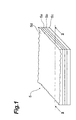
- Fig. 1 is a perspective view of a cathode depicting a preferred embodiment of the cathode for photo-electron emission.
- the cathode for photo-electron emission 5 (cathode for photo-electron emission) is comprised of (2) metal layer 5b, (3) intermediate layer 5a, and (4) alkali metal containing layer (photo-electric face: thin film) 5d, which are sequentially layered on (1) substrate 5c.
- the description follows.
- the surface of the substrate 5c may be mildly oxidized.
- the metal layer 5b is made of Al, and this Al, which functions as a reflection film when light enters, may be Ni.
- the cathode for photo-electron emission 5, in this example, is a reflection type, but the cathode 5 may be a transmission type where the intermediate layer 5a and the alkali metal containing layer 5d are sequentially formed on the substrate 5c having a translucency, such as glass or sapphire.
- An oxide layer of manganese (manganese oxide) maybe formed between the substrate 5c and intermediate layer 5a.
- the intermediate layer 5a is a layer containing carbon, and is comprised of carbon nano-tubes in this example.
- a carbon nano-tube is a cylindrical material where one layer of graphite (graphine) is rolled into a cylinder.
- the primary cylindrical material, all made of carbon atoms, are micro-crystals which diameter is about 0.5 nm to 10 nm, and the length is about 1 ⁇ m.
- One nano-tube normally has a special structure called a "helical structure".
- a method for layering the intermediate layer 5a made of carbon nano-tubes on the Al layer 5b is not especially limited, but, for example, may involve dropping a predetermined amount of a suspended carbon nano-tube solution, where carbon nano-tubes are suspended or dispersed in such a solvent as alcohol, on the Al layer 5b, and removing the solvent by drying.
- the thickness of the intermediate layer 5a is not especially limited if the particles of carbon nano-tubes are evenly deposited on at least one layer.
- the shape of a carbon nano-tube to be used is not limited, and may, for example, be a normally synthesized carbon nano-tube which diameter is about 0.1 - several tens nm, and the length is about 1 ⁇ m or less.
- the above mentioned (n, m) shows the chiral vector (where 0 ⁇
- the deposition direction of the particles of the carbon nano-tube is not especially limited either. In other words, the longitudinal direction of a carbon nano-tube having a cylindrical shape, such as a needle shape, and the plane of the Al layer 5b, may be in parallel or form an angle .
- such carbon material as graphite, amorphous carbon, or fullerene of carbon may be used alone or together with carbon nano-tubes with or without mixing, but it is preferable that a carbon nano-tube is the main component.
- the particle diameter of such a carbon material is preferably similar to the above mentioned diameter of a carbon nano-tube or less.
- the alkali metal containing layer 5d (photo-electric face: thin film) is comprised of grown and deposited particles which emit photo-electrons by the entry of light or which emit secondary electrons by the entry of electrons.
- photo-electric face and “secondary electron emitting face” show the entire thin film having a predetermined thickness, where particles or particulate matter are deposited or combined, that is, the alkali metal containing layer 5d.
- the material of the particles constituting the alkali metal containing layer 5d is preferably a metal compound containing at least one metal element selected from groups comprised of such alkali metal as cesium (Cs), sodium (Na), potassium (K), and antimony (Sb), that is, an alkali antimony compound.
- Cs cesium
- Na sodium
- K potassium
- Sb antimony
- Micro-bumps are formed on the surface of the alkali metal containing layer 5d by the particles. It is preferable that the average particle diameter is about the diffusion length of a photo-electron, that is, about 500 nm, for example, and the height from the concave part to the convex part on the surface of the alkali metal containing layer 5d is about 1000 nm, and the space between the convex parts (or concave parts) is about 1000 nm.
- the alkali metal containing layer 5d comprised of many particles can be formed by normal vapor phase epitaxy, where an alkali metal stream is reacted with Sb particulate film deposited in an inactive gas, such as argon (Ar), Neon (Ne), or hydrogen (H 2 ).
- an inactive gas such as argon (Ar), Neon (Ne), or hydrogen (H 2 ).
- Fig. 2 is an enlarged cross-sectional view depicting the structure of the II-II cross-section in Fig. 1.
- Fig. 2 shows, in the cathode for photo-electron emission 5, particles contacting the intermediate layer 5a do not deform to a flat state (status of the prior art shown in Fig. 9), and the particles 2 have an elliptical shape.
- the contact area between the intermediate layer 5a and the particle 2 contacting on the surface thereof is smaller than prior art.
- the degree of contact between the particles 2 and the intermediate layer 5a is less than prior art, so the strain stress to be applied when crystals of the particles 2 grow decreases, and as Fig. 2 shows, the generation of crystal defects 6 inside the particles 2 and propagation thereof are controlled, as shown in Fig. 2. Therefore defects which extend inside the particles 2 which are sequentially grown and deposited on the particles 2 are decreased. Since the density of crystal defects 6 inside the particles 2 in the entire alkali metal containing layer 5d is decreased, the recombining probability between electrons excited by light or electrons and holes decreases remarkably. As a result, the decrease of excited electrons which reach the surface of the particles 2 is controlled, so quantum efficiency can be improved, and the spectral sensitivity characteristic thereof can be improved compared with prior art.
- the intermediate layer 5a is comprised of carbon nano-tubes, and micro-bumps having a curvature in the micro-pore order, or sub-micro-pore order to meso-pore order, can be formed on the surface of the intermediate layer 5a (interface with the particles 2) by the layering of carbon nano-tubes. Therefore wettability of the intermediate layer 5a with respect to the particles 2 sufficiently drops, and particles 2 tend to be deposited in an elliptical shape. As a result, the density of crystal defects 6 inside the particles further decreases. So the quantum efficiency of a cathode for photo-electron or secondary electron emission can be further increased, and spectral sensitivity thereof can be further improved.
- a preferable embodiment of the cathode for secondary electron emission is one having a configuration similar to the cathode for photo-electron emission 5 shown in Fig. 1.
- the alkali metal containing layer 5d is the primary electron entering face (secondary electron emitting face), where incident primary electrons reflected by the cathode surface also enter the cathode for secondary electron emission, and contribute to secondary electron emission.
- Fig. 3 is a cross-sectional view of a photo-electric tube depicting an embodiment of the photo-electric tube using the above mentioned cathode for photo-electron emission 5 as a reflection type photo-electric cathode.
- the photo-electric tube 10 is a cathode for photo-electron emission 5, anode 8 comprised of Ni, and lead-in wire 9 installed in the glass cylinder 7, which is a vacuum container.
- incident light 1 which is photons to be detected, enters the alkali metal containing layer 5d of the cathode for photo-electron emission 5, photo-electrons are emitted which generates photo-electric current, and photo-electric current is scavenged by the anode 8.
- the photo-electric tube 10 the quantum efficiency of the cathode for photo-electron emission is increased and the spectral sensitivity characteristic is improved, as described above, so high sensitive photo-detection becomes possible.
- the cathode 5 can be used as a photo-electric cathode, and can also be used as a dynode, as described below.
- Fig. 4 is a cross-sectional view of a photomultiplier depicting an embodiment of the photomultiplier where the above cathode 5 is used as a dynode.
- the photomultiplier 100 is a transmission type multi-alkali photo-electric face (photo-electric cathode material) 12 formed inside the window section of the glass cylinder 7 (vacuum container), where the electron entering face of the cathode 5 is curved.
- the cathode 5 is installed inside the glass cylinder 7.
- the cathode 5 is a cathode for secondary electron emission 5 where the alkali metal containing layer 5d is formed on the Ni electrode substrate 5c on which the Al layer 5b is deposited via the intermediate layer 5a comprised of carbon nano-tubes. This is for secondary electron emission, but the structure thereof is the same as the above cathode for photo-electron emission. To avoid redundant descriptions, descriptions of the detailed parts of the composing elements are omitted here.
- the cathode for secondary electron emission 5 is installed so that the alkali metal containing layer 5d comes to the (primary) electron entering side, and the lead pin 9a is electrically connected to the Ni electrode substrate 5c. Also on the multi-alkali photo-electric face 12, the lead pin 9b and the focusing electrode 14 are electrically connected, and the anode 8 comprised of Ni is also installed inside the glass cylinder 7.
- the incident light 1 which is light to be detected, is converted into photo-electrons 15 by the multi-alkali photo-electric face 12.
- These photo-electrons 15 are accelerated, focused, and enter the cathode for secondary electron emission 5, where the photo-electrons 15 are further multiplied and scavenged by the anode 8.
- the secondary electron emission efficiency of the cathode for secondary electron emission 5 is increased, as described above, so the electron multiplication characteristic is superb, and the amplification rate of incident photons improves, therefore high sensitive light detection is possible.
- Fig. 5 is a cross-sectional view of a multiplier depicting an embodiment of the electronic multiplier.
- the electronic multiplier 200 is configured such that the above mentioned cathodes for secondary electron emission 5 are disposed in multiple stages as dynodes inside the body 71 (container) which has an opening to which the (primary) electrons 17 can enter, where the anode 81 is installed at the rear side of the cathode for secondary electron emission at the last stage or nearby.
- the cathode for secondary electron emission 5 shown in Fig. 5 has the layered structure shown in Fig. 4, except that the shape has a predetermined curvature .
- a potential lower than that for anode 81 is supplied to each cathode for secondary electron emission 5.
- the electronic multiplier 200 with such a configuration is installed, for example, in the chamber 30, which internal pressure is reduced to a predetermined degree of vacuum.
- An electron emission source 40 is installed in the chamber 30, and the primary electrons 17 emitted from the electron emission source 40 enter inside through the opening of the electronic multiplier 200.
- the primary electrons 17 are focused by the focusing electrode 14 and enter the cathode for secondary electron emission 5 at the first stage, secondary electrons are emitted.
- incidence and emission are repeated while being multiplied by the cathode for secondary electron emission 5 in a subsequent stage, and the electrons emitted from the cathode for secondary electron emission 5 at the last stage enter the anode 81.
- Such an electronic multiplier 200 can be suitably applied to the electronic multiplier in an electron microscope, for example.
- this electronic multiplier 200 the secondary electron emission characteristic of the cathode for secondary electron emission 5 has been improved, so the electron multiplication characteristic is superb, and the amplification rate of the primary electrons 17 to enter can be improved.
- an object in a field of view of an electron microscope, for example, can be observed at higher sensitivity.
- the photomultiplier 100 can be configured as the photomultiplier according to the present invention.
- a layer comprised of suchmetal as Cr maybe created between the intermediate layer 5a and the Al layer 5b of the cathode for photo-electron emission 5. Then the reflectance of incident light can be further increased by preventing contamination and scratches, and the reaction between Ni of the Ni electrode substrate 5c and Sb of the alkali metal containing layer 5d can be sufficiently prevented by introducing the Cr layer.
- a material activation method e.g. temperature, time, amount of alkali metal, sequence
- a material activation method e.g. temperature, time, amount of alkali metal, sequence
- the cathode face and the dynode face of the thin film of the photo-electric face are matched at the maximum sensitivity point. Therefore it is preferable to optimize the balance of the Sb amount and the alkali metal amount of both the cathode face and dynode face.
- the photo-electric tube 10 with the structure in Fig. 3 was created according to the following procedure.
- a conventional cathode for photo-electron emission 25 (see Fig. 8), where the porous Sb particulate film is directly formed on the Al layer 5b without the intermediate layer 5a, was fabricated in the same way as the above mentioned Example 1, except in this case step (2) in Example 1 was not executed, and the photo-electric tube was obtained.
- step (2) in Example 1 was not executed, and the photo-electric tube was obtained.
- Spectral sensitivity was measured for the cathode for photo-electron emission of the photo-electric tubes fabricated in Example 1 and Comparison 1.
- Fig. 6 is a graph depicting the quantum efficiency of the photo-electric tubes fabricated in Example 1 and Comparison 1, with respect to the incident light wavelength, where the curves L1 and L2 show the spectral quantum efficiency of the photo-electric tubes of Example 1 and Comparison 1 respectively.
- Fig. 6 shows, it was confirmed that the quantum efficiency of the cathode for photo-electron emission of the present invention has been improved dramatically compared with prior art in the range of wavelengths of about 600 to 850 nm (red - near infra-red region).
- the quantum efficiency at around wavelength 750 nm (red sensitivity), in particular, is about 1.8 times that of prior art.
- the quantum efficiency of the cathode for photo-electron emission of the present invention becomes slightly lower than prior art, but as described above, the quantum efficiency in the red region (red sensitivity) is improved dramatically, and in the sensitivity wavelength region in general, the flatness (uniformity) of sensitivity of the present invention is better than prior art. Therefore from this aspect, it was confirmed that the spectral sensitivity characteristic is improved by the present invention.
- the photomultiplier 100 with the same structure shown in Fig. 4 was fabricated.
- a conventional electric multiplier was fabricated in the same way as Example 2, except that a cathode for photo-electron emission having the same configuration as the above mentioned Comparison 1 is used as the cathode for secondary electron emission 13, shown in Fig. 4 in this case.
- the secondary electron emission characteristic was measured for the cathode for secondary electron emission of the photomultipliers fabricated in Example 2 and Comparison 2.
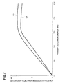
- Fig. 7 is a graph depicting the secondary electron emission efficiency with respect to the primary electron energy of the electronic multipliers fabricated in Example 2 and Comparison 2, where the curves L3 and L4 show the secondary electron emission efficiency of the photo-electric tubes of Example 2 and Comparison 2 respectively. As Fig. 7 shows, it was confirmed that the secondary electron emission efficiency of the electronic multiplier of the present invention improved remarkably compared with prior art.
- the quantum efficiency can be improved compared with prior art, particularly the quantum efficiency with respect to incident light having a wavelength primarily in the red region (red sensitivity) can be improve dramatically, since the quantum efficiency in the red region can be improved, and the flatness of the spectral sensitivity in the entire sensitivity wavelength region can be improved, the spectral sensitivity characteristic can be sufficiently improved.
- an electrode for secondary electron emission where secondary electron emission efficiency is improved much more than prior art, can be obtained.
- a photomultiplier and electronic multiplier with an extremely superb photo-electron emission characteristic and secondary electron emission characteristic can be obtained using the cathodes for photo-electron and secondary electron emission of the present invention.
- the present invention can be used for an electron emission cathode and photomultiplier.
Landscapes
- Engineering & Computer Science (AREA)
- Chemical & Material Sciences (AREA)
- Nanotechnology (AREA)
- Physics & Mathematics (AREA)
- Mathematical Physics (AREA)
- Theoretical Computer Science (AREA)
- Crystallography & Structural Chemistry (AREA)
- Common Detailed Techniques For Electron Tubes Or Discharge Tubes (AREA)
Abstract
Description
- The present invention relates to an electron emitting cathode for emitting photo-electrons or secondary electrons, and this cathode is applied to a photomultiplier, for example.
- A conventional cathode for photo-electron or secondary electron emission is, for example, one stated in the Official Gazette on Japanese Patent Laid-Open No. 6-119872 (registered patent No. 2651329) claimed by the present applicant.
- Fig. 8 is a perspective view depicting an example of this conventional cathode for photo-electron emission. The cathode for photo-
electron emission 25 is comprised of athin film 25d, where compound particles of alkali metal and antimony (Sb) are deposited on a nickel (Ni)electrode substrate 25c covered with an aluminum (Al)layer 25b. In this conventional cathode for photo-electron emission, the diameter of a particle constituting thethin film 25d is about the diffusion wavelength of an excited electron, where an improvement of electron emission efficiency (quantum efficiency) has been intended. - In a cathode for photo-electron emission, quantum efficiency normally depends on wavelength. In the case of a device using a cathode for photo-electron emission for detecting light, electrons or other charged particles, such as a photomultiplier, high quantum efficiency is generally desired in the entire wavelength region of the detection target or in a particle energy region wider than this area. In many cases, high quantum efficiency (red sensitivity) for wavelengths of about 600 to 800 nm of red to near infra-red is demanded. Whereas in the above mentioned conventional cathode for photo-electron emission, sensitivity in the wavelength region of about 600 to 800 nm is relatively low, and further improvement of red sensitivity has been desired.
- With the foregoing in view, it is an object of the present invention to provide a cathode for photo-electron or secondary electron emission where quantum efficiency, particularly red sensitivity, can be improved, and the spectral sensitivity (photo-electron emission characteristic) or the secondary electron emission characteristic is improved. It is another object of the present invention to provide a photomultiplier and electronic multiplier having an excellent photo-electron emission characteristic or secondary electron emission characteristic.
- To solve the above problems, the present inventors have eagerly researched the crystal particle growth process and film characteristics of a conventional cathode for photo-electron emission, where a thin film comprised of crystal particles of alkali antimony compound semiconductor is formed on an Al deposited substrate, and as a result the following was found out.
- Fig. 9 is an enlarged cross-sectional view depicting the structure of the cathode for photo-
electron emission 25 in Fig. 8 in cross-section IX-IX. As Fig. 9 shows, strain stress, which is generated by the differences of the thermal expansion coefficient and lattice constant with theNi electrode substrate 25c, is applied to theparticles 20 contacting theAl film 25b, andcrystal defects 26 are generated as a result of relaxing this stress. - Here in the cathode for photo-
electron emission 25, the cross-section of theparticles 20 at the contact area tends to flatten due to the wettability between theAl film 25b and theparticles 20. If this occurs, the strain stress applied to theparticles 20 is increased, and the density of crystal defects 26 (defect density) increases. Also inside the particles which grow on thecrystal particles 20 at the contact area, defects originating from a line defect or plane defect of the particles below are sequentially generated, and the defect density of anentire crystal particle 20 increases. In acrystal defect 26, the probability that an electron, excited by light or electrons, will recombine with a hole increases, and excited electrons which reach the surface of thecrystal grain 20 decreases, which drops the quantum efficiency. The present inventors further promoted research based on these findings, and completed the present invention. - The present cathode for photo-electron or secondary electron emission is a cathode for photo-electron or secondary electron emission, comprising a thin film made of a material for emitting photo-electrons by the entry of light or for emitting secondary electrons by the entry of electrons, preferably a compound of at least one type of alkali metal and antimony metal, is formed on a substrate, characterized in that an intermediate layer comprised of carbon is disposed between the thin film and the substrate.
- In the case of a cathode for photo-electron or secondary electron emission configured like this, a thin film, as a photo-electron emitting face, or a secondary electron emitting face for emitting photo-electrons or secondary electrons, is formed on the intermediate layer comprised of carbon disposed on the substrate. If this thin film is formed by depositing particles comprised of the above mentioned material for emitting photo-electrons or secondary electrons, photo-electrons or secondary electrons are emitted from the particles when light or primary electrons enter the particles constituting the thin film. Here it was found out that the deposited particles contacting the intermediate layer do not flatten, but maintain an elliptical shape, unlike prior art. The mechanism for such an interaction is not sufficiently understood, but it was confirmed that strain stress to be applied to the particles during particle growth is decreased, and internal crystal defects decrease.
- Since the defect density of particles at the contact section with the intermediate layer decreases, defects which extend the crystal defects of the particles below are decreased in the grains which grow on the particles at the contact section. Therefore the crystal defect density in the particles of the entire thin film decreases the recombining probability of electrons excited by light or electrons and holes decreases remarkably, and the decrease of excited electrons reaching the surface of particles is controlled. Also even if the thin film is not formed by deposition of individually separated independent particles or particulate matter, and has such a deposition structure where many particles are connected together, or are in a state close to the film, crystal defects can be decreased since the above mentioned strain stress decreases.
- It is preferable that the intermediate layer contains carbon nano-tubes. On the surface of the intermediate layer where particles of carbon nano-tubes are layered, micro-bumps in a nano-meter order are created. Such a shape and material characteristic drops wettability on the surface of the intermediate layer with respect to the particles constituting the thin film, which further controls the particles constituting the thin film to be deposited in a flattened state (such an interaction is not limited to this). As a result, the defect density in particles is further decreased, where the recombining probability of electrons and holes is further dropped, and the decrease of excited electrons which reaches the particle surface is further controlled.
- It is also preferable that the thin film is activated by alkali metal, or that the thin film is comprised of a compound (alkali antimony compound) which consists of at least one type of alkali metal and antimony (Sb), particularly bi-alkali or a multi-alkali antimony compound.
- The present photomultiplier or electronic multiplier has the above mentioned cathode for photo-electron emission or a cathode for secondary electron emission respectively. In other words, the present photomultiplier is characterized in that the above mentioned cathode for photo-electron emission is installed inside a vacuum container which has a light entrance window, where photo-electrons, which are emitted from the cathode for photo-electron emission by the incident light, are multiplied inside the vacuum container. The secondary electron multiplier is characterized in that the cathode for secondary electron emission of the present invention is installed in stages inside the container, where electrons to be detected enter the cathode for secondary electron emission at the first stage, and the secondary electrons emitted by the cathode for secondary electron emission at the last stage enter the anode. The "vacuum container" is a sealed container where pressure inside the container is reduced to be roughly a vacuum.
-
- Fig. 1 is a perspective view of a cathode depicting a preferred embodiment of the cathode for photo-electron emission;
- Fig. 2 is an enlarged cross-sectional view of a cathode depicting the structure of the cathode for photo-electron emission;
- Fig. 3 is a cross-sectional view of a photo-electric tube depicting an embodiment of a photo-electronic tube where the cathode for electron emission is used as a reflection type photo-electric cathode;
- Fig. 4 is a cross-sectional view of a photomultiplier depicting an embodiment of a photomultiplier where the cathode for electron emission is used as a dynode;
- Fig. 5 is a cross-sectional view of an electronic multiplier depicting an embodiment of the electronic multiplier;
- Fig. 6 is a graph depicting the quantum efficiency
of the photo-electric tube (photomultiplier) of Example 1
and
Comparison 1 with respect to the wavelength of the incident light; - Fig. 7 is a graph depicting the secondary electron
emission efficiency of the photomultiplier of Example 2 and
Comparison 2 with respect to the primary electron energy; - Fig. 8 is a perspective view of a cathode depicting an example of a conventional cathode for photo-electron emission; and
- Fig. 9 is an enlarged cross-sectional view depicting the structure of a conventional cathode for photo-electron emission.
-
- Embodiments of the present invention will now be described with reference to the accompanying drawings. The same composing elements are denoted with the same symbols, where redundant descriptions are omitted.
- Fig. 1 is a perspective view of a cathode depicting a preferred embodiment of the cathode for photo-electron emission. The cathode for photo-electron emission 5 (cathode for photo-electron emission) is comprised of (2)
metal layer 5b, (3)intermediate layer 5a, and (4) alkali metal containing layer (photo-electric face: thin film) 5d, which are sequentially layered on (1)substrate 5c. The description follows. - This is a substrate made of
substrate 5c metal, and the metal is made of Ni, in this example, but may be Al or stainless. The surface of thesubstrate 5c may be mildly oxidized. - The
metal layer 5b is made of Al, and this Al, which functions as a reflection film when light enters, may be Ni. The cathode for photo-electron emission 5, in this example, is a reflection type, but thecathode 5 may be a transmission type where theintermediate layer 5a and the alkalimetal containing layer 5d are sequentially formed on thesubstrate 5c having a translucency, such as glass or sapphire. An oxide layer of manganese (manganese oxide) maybe formed between thesubstrate 5c andintermediate layer 5a. - The
intermediate layer 5a is a layer containing carbon, and is comprised of carbon nano-tubes in this example. A carbon nano-tube is a cylindrical material where one layer of graphite (graphine) is rolled into a cylinder. The primary cylindrical material, all made of carbon atoms, are micro-crystals which diameter is about 0.5 nm to 10 nm, and the length is about 1 µm. One nano-tube normally has a special structure called a "helical structure". - A method for layering the
intermediate layer 5a made of carbon nano-tubes on theAl layer 5b is not especially limited, but, for example, may involve dropping a predetermined amount of a suspended carbon nano-tube solution, where carbon nano-tubes are suspended or dispersed in such a solvent as alcohol, on theAl layer 5b, and removing the solvent by drying. And the thickness of theintermediate layer 5a is not especially limited if the particles of carbon nano-tubes are evenly deposited on at least one layer. Also the shape of a carbon nano-tube to be used is not limited, and may, for example, be a normally synthesized carbon nano-tube which diameter is about 0.1 - several tens nm, and the length is about 1 µm or less. - The stereoscopic structure of the carbon nano-tube is not limited either, where any one of a chiral tube type (n, m: n≠m and m≠0), arm chair type (n, m: n = m) , and zigzag tube type (n, m: m = 0) may be used, and carbon nano-tubes having these stereoscopic structures may be mixed. The above mentioned (n, m) shows the chiral vector (where 0≤ | n | ≤m |. The deposition direction of the particles of the carbon nano-tube is not especially limited either. In other words, the longitudinal direction of a carbon nano-tube having a cylindrical shape, such as a needle shape, and the plane of the
Al layer 5b, may be in parallel or form an angle . - For the material of the
intermediate layer 5a, such carbon material as graphite, amorphous carbon, or fullerene of carbon (e.g. C60, C70, C84) may be used alone or together with carbon nano-tubes with or without mixing, but it is preferable that a carbon nano-tube is the main component. The particle diameter of such a carbon material is preferably similar to the above mentioned diameter of a carbon nano-tube or less. - The alkali
metal containing layer 5d (photo-electric face: thin film) is comprised of grown and deposited particles which emit photo-electrons by the entry of light or which emit secondary electrons by the entry of electrons. In the description, "photo-electric face" and "secondary electron emitting face" show the entire thin film having a predetermined thickness, where particles or particulate matter are deposited or combined, that is, the alkalimetal containing layer 5d. - The material of the particles constituting the alkali
metal containing layer 5d is preferably a metal compound containing at least one metal element selected from groups comprised of such alkali metal as cesium (Cs), sodium (Na), potassium (K), and antimony (Sb), that is, an alkali antimony compound. - Micro-bumps are formed on the surface of the alkali
metal containing layer 5d by the particles. It is preferable that the average particle diameter is about the diffusion length of a photo-electron, that is, about 500 nm, for example, and the height from the concave part to the convex part on the surface of the alkalimetal containing layer 5d is about 1000 nm, and the space between the convex parts (or concave parts) is about 1000 nm. - The alkali
metal containing layer 5d comprised of many particles can be formed by normal vapor phase epitaxy, where an alkali metal stream is reacted with Sb particulate film deposited in an inactive gas, such as argon (Ar), Neon (Ne), or hydrogen (H2). - The photo-electron emission mechanism by such an alkali
metal containing layer 5d is described in detail in Japanese Patent Laid-Open 6-119872 (registered patent No. 2651329) by the present applicant. - Fig. 2 is an enlarged cross-sectional view depicting the structure of the II-II cross-section in Fig. 1.
- As Fig. 2 shows, in the cathode for photo-
electron emission 5, particles contacting theintermediate layer 5a do not deform to a flat state (status of the prior art shown in Fig. 9), and theparticles 2 have an elliptical shape. The contact area between theintermediate layer 5a and theparticle 2 contacting on the surface thereof is smaller than prior art. - The principle where the
particles 2 contacting theintermediate layer 5a do not become a flat state, unlike prior art, in the alkalimetal containing layer 5d constituting such a cathode for photo-electron emission 5, has not yet been clearly understood, but can be assumed to be as follows. - One presumption is that wettability on the surface of the
intermediate layer 5 with respect to theparticle 2 becomes lower than prior art, which does not have theintermediate layer 5a, because of the relationship of the surface free energy between theintermediate layer 5a comprised of carbon nano-tubes and theparticles 2. It is also presumed that the surface free energy of theintermediate layer 5a depends on material characteristics and/or shape, and one reason is that the material of theintermediate layer 5a is carbon, and a micro-curvature in a nano-meter order is generated on the surface of theintermediate layer 5a. - Another possible reason is that the strain stress applied to the
particles 2 is relaxed by theintermediate layer 5a, and the surface tension of theintermediate layer 5a (interfacial tension with particles 2) is increased, which accelerates the condensation of particles. The interactions, however, are not limited to these. - Conventionally a carbon material, such as graphite, has been difficult to use for a cathode having a photo-electric face containing alkali metal, because of the intercalation effect, which takes heterogeneous atoms into a layered structure. However if an
intermediate layer 5a comprised of carbon is created, crystal defects in theparticles 2 are decreased, and sensitivity is improved, as mentioned later, regardless which one of the above mentioned interactions is dominant. - According to the cathode for photo-
electron emission 5 having such a configuration, the degree of contact between theparticles 2 and theintermediate layer 5a is less than prior art, so the strain stress to be applied when crystals of theparticles 2 grow decreases, and as Fig. 2 shows, the generation ofcrystal defects 6 inside theparticles 2 and propagation thereof are controlled, as shown in Fig. 2. Therefore defects which extend inside theparticles 2 which are sequentially grown and deposited on theparticles 2 are decreased. Since the density ofcrystal defects 6 inside theparticles 2 in the entire alkalimetal containing layer 5d is decreased, the recombining probability between electrons excited by light or electrons and holes decreases remarkably. As a result, the decrease of excited electrons which reach the surface of theparticles 2 is controlled, so quantum efficiency can be improved, and the spectral sensitivity characteristic thereof can be improved compared with prior art. - Also the
intermediate layer 5a is comprised of carbon nano-tubes, and micro-bumps having a curvature in the micro-pore order, or sub-micro-pore order to meso-pore order, can be formed on the surface of theintermediate layer 5a (interface with the particles 2) by the layering of carbon nano-tubes. Therefore wettability of theintermediate layer 5a with respect to theparticles 2 sufficiently drops, andparticles 2 tend to be deposited in an elliptical shape. As a result, the density ofcrystal defects 6 inside the particles further decreases. So the quantum efficiency of a cathode for photo-electron or secondary electron emission can be further increased, and spectral sensitivity thereof can be further improved. - A preferable embodiment of the cathode for secondary electron emission is one having a configuration similar to the cathode for photo-
electron emission 5 shown in Fig. 1. In this case, the alkalimetal containing layer 5d is the primary electron entering face (secondary electron emitting face), where incident primary electrons reflected by the cathode surface also enter the cathode for secondary electron emission, and contribute to secondary electron emission. - Fig. 3 is a cross-sectional view of a photo-electric tube depicting an embodiment of the photo-electric tube using the above mentioned cathode for photo-
electron emission 5 as a reflection type photo-electric cathode. - The photo-
electric tube 10 is a cathode for photo-electron emission 5,anode 8 comprised of Ni, and lead-inwire 9 installed in theglass cylinder 7, which is a vacuum container. In the photo-electric tube 10 with such a configuration,incident light 1, which is photons to be detected, enters the alkalimetal containing layer 5d of the cathode for photo-electron emission 5, photo-electrons are emitted which generates photo-electric current, and photo-electric current is scavenged by theanode 8. By the photo-electric tube 10, the quantum efficiency of the cathode for photo-electron emission is increased and the spectral sensitivity characteristic is improved, as described above, so high sensitive photo-detection becomes possible. Also a photomultiplier is created if an electronic-multiplying section is installed between thecathode 5 and theanode 8. In the photomultiplier, thecathode 5 can be used as a photo-electric cathode, and can also be used as a dynode, as described below. - Fig. 4 is a cross-sectional view of a photomultiplier depicting an embodiment of the photomultiplier where the
above cathode 5 is used as a dynode. Thephotomultiplier 100 is a transmission type multi-alkali photo-electric face (photo-electric cathode material) 12 formed inside the window section of the glass cylinder 7 (vacuum container), where the electron entering face of thecathode 5 is curved. - The
cathode 5 is installed inside theglass cylinder 7. Thecathode 5 is a cathode forsecondary electron emission 5 where the alkalimetal containing layer 5d is formed on theNi electrode substrate 5c on which theAl layer 5b is deposited via theintermediate layer 5a comprised of carbon nano-tubes. This is for secondary electron emission, but the structure thereof is the same as the above cathode for photo-electron emission. To avoid redundant descriptions, descriptions of the detailed parts of the composing elements are omitted here. - The cathode for
secondary electron emission 5 is installed so that the alkalimetal containing layer 5d comes to the (primary) electron entering side, and thelead pin 9a is electrically connected to theNi electrode substrate 5c. Also on the multi-alkali photo-electric face 12, thelead pin 9b and the focusingelectrode 14 are electrically connected, and theanode 8 comprised of Ni is also installed inside theglass cylinder 7. - In the
photomultiplier 100 with such a configuration, theincident light 1, which is light to be detected, is converted into photo-electrons 15 by the multi-alkali photo-electric face 12. These photo-electrons 15 are accelerated, focused, and enter the cathode forsecondary electron emission 5, where the photo-electrons 15 are further multiplied and scavenged by theanode 8. By thephotomultiplier 100, the secondary electron emission efficiency of the cathode forsecondary electron emission 5 is increased, as described above, so the electron multiplication characteristic is superb, and the amplification rate of incident photons improves, therefore high sensitive light detection is possible. - Fig. 5 is a cross-sectional view of a multiplier depicting an embodiment of the electronic multiplier. The
electronic multiplier 200 is configured such that the above mentioned cathodes forsecondary electron emission 5 are disposed in multiple stages as dynodes inside the body 71 (container) which has an opening to which the (primary)electrons 17 can enter, where theanode 81 is installed at the rear side of the cathode for secondary electron emission at the last stage or nearby. - Inside the opening of the
body 71, the focusingelectrode 14, where thelead pin 9b extending to outside thecontainer 30 is electrically connected, is installed, so that theprimary electrons 17 are focused and enter the cathode forsecondary electron emission 5 at the first stage. The cathode forsecondary electron emission 5 shown in Fig. 5 has the layered structure shown in Fig. 4, except that the shape has a predetermined curvature . A potential lower than that foranode 81 is supplied to each cathode forsecondary electron emission 5. - The
electronic multiplier 200 with such a configuration is installed, for example, in thechamber 30, which internal pressure is reduced to a predetermined degree of vacuum. Anelectron emission source 40 is installed in thechamber 30, and theprimary electrons 17 emitted from theelectron emission source 40 enter inside through the opening of theelectronic multiplier 200. When theprimary electrons 17 are focused by the focusingelectrode 14 and enter the cathode forsecondary electron emission 5 at the first stage, secondary electrons are emitted. For these secondary electrons, incidence and emission are repeated while being multiplied by the cathode forsecondary electron emission 5 in a subsequent stage, and the electrons emitted from the cathode forsecondary electron emission 5 at the last stage enter theanode 81. - Such an
electronic multiplier 200 can be suitably applied to the electronic multiplier in an electron microscope, for example. According to thiselectronic multiplier 200, the secondary electron emission characteristic of the cathode forsecondary electron emission 5 has been improved, so the electron multiplication characteristic is superb, and the amplification rate of theprimary electrons 17 to enter can be improved. As a result, an object in a field of view of an electron microscope, for example, can be observed at higher sensitivity. - If the above mentioned transmission type cathode for photo-electron emission is used as the multi-alkali photo-
electric face 12, then thephotomultiplier 100 can be configured as the photomultiplier according to the present invention. - Also a layer comprised of suchmetal as Cr maybe created between the
intermediate layer 5a and theAl layer 5b of the cathode for photo-electron emission 5. Then the reflectance of incident light can be further increased by preventing contamination and scratches, and the reaction between Ni of theNi electrode substrate 5c and Sb of the alkalimetal containing layer 5d can be sufficiently prevented by introducing the Cr layer. - To increase the sensitivity of the photomultiplier or the electronic multiplier, a material activation method (e.g. temperature, time, amount of alkali metal, sequence) of the material to be used for the alkali
metal containing layer 5d can be appropriately adjusted. In terms of increasing sensitivity, it is preferable that the cathode face and the dynode face of the thin film of the photo-electric face are matched at the maximum sensitivity point. Therefore it is preferable to optimize the balance of the Sb amount and the alkali metal amount of both the cathode face and dynode face. - The present invention will now be further described using examples, but the present invention is not limited to these examples.
- The photo-
electric tube 10 with the structure in Fig. 3 was created according to the following procedure. - (1) Al is deposited on the
Ni electrode substrate 5c (thickness: 0.127 mm) to form theAl layer 5b (thickness: 100 nm). - (2) A solution of carbon nano-tubes (made by Nippon Yakin,
product name: Carbon Nano-tube Type 2 (high content powder) )
mixed with ethanol is dropped on the
Al layer 5b, then ethanol is evaporated to form theintermediate layer 5a (maximum deposition thickness about 80 nm). - (3) Sb is deposited on the
intermediate layer 5a in a hydrogen gas atmosphere to form a porous Sb particulate film. - (4) The above is incorporated into the
glass cylinder 7, shown in Fig. 3, the pressure inside theglass cylinder 7 is reduced to be roughly a vacuum, and alkali metal (K, Na, Cs) steam is reacted with the porous Sb particulate film to form the alkalimetal containing layer 5d, and as a result, the cathode for photo-electron emission 5, comprised of a multi-alkali antimony compound, is obtained. - (5) Then the
glass cylinder 7 is hermetically sealed, and the photo-electric tube 10 is obtained. -
- As a result of observing the obtained alkali
metal containing layer 5d using a scanning electron microscope (SEM), it was confirmed that the multi-alkali particles in the alkalimetal containing layer 5d was deposited in a shape closer to elliptical than that of a flattened state. - A conventional cathode for photo-electron emission 25 (see Fig. 8), where the porous Sb particulate film is directly formed on the
Al layer 5b without theintermediate layer 5a, was fabricated in the same way as the above mentioned Example 1, except in this case step (2) in Example 1 was not executed, and the photo-electric tube was obtained. As a result of observing the photo-electric face in this conventional photo-electric tube using SEM, it was confirmed that the multi-alkali particles on the photo-electric face deposited on the Al layer in a flat state. - Spectral sensitivity was measured for the cathode for photo-electron emission of the photo-electric tubes fabricated in Example 1 and
Comparison 1. Fig. 6 is a graph depicting the quantum efficiency of the photo-electric tubes fabricated in Example 1 andComparison 1, with respect to the incident light wavelength, where the curves L1 and L2 show the spectral quantum efficiency of the photo-electric tubes of Example 1 andComparison 1 respectively. - As Fig. 6 shows, it was confirmed that the quantum efficiency of the cathode for photo-electron emission of the present invention has been improved dramatically compared with prior art in the range of wavelengths of about 600 to 850 nm (red - near infra-red region). The quantum efficiency at around wavelength 750 nm (red sensitivity), in particular, is about 1.8 times that of prior art.
- At a wavelength of about 400 nm or less, however, the quantum efficiency of the cathode for photo-electron emission of the present invention becomes slightly lower than prior art, but as described above, the quantum efficiency in the red region (red sensitivity) is improved dramatically, and in the sensitivity wavelength region in general, the flatness (uniformity) of sensitivity of the present invention is better than prior art. Therefore from this aspect, it was confirmed that the spectral sensitivity characteristic is improved by the present invention.
- Using the cathode for photo-electron emission, having the same layer configuration as the above mentioned Example 1, as the cathode for
secondary electron emission 5 shown in Fig. 4, thephotomultiplier 100 with the same structure shown in Fig. 4 was fabricated. - A conventional electric multiplier was fabricated in the same way as Example 2, except that a cathode for photo-electron emission having the same configuration as the above mentioned
Comparison 1 is used as the cathode for secondary electron emission 13, shown in Fig. 4 in this case. - The secondary electron emission characteristic was measured for the cathode for secondary electron emission of the photomultipliers fabricated in Example 2 and
Comparison 2. - Fig. 7 is a graph depicting the secondary electron emission efficiency with respect to the primary electron energy of the electronic multipliers fabricated in Example 2 and
Comparison 2, where the curves L3 and L4 show the secondary electron emission efficiency of the photo-electric tubes of Example 2 andComparison 2 respectively. As Fig. 7 shows, it was confirmed that the secondary electron emission efficiency of the electronic multiplier of the present invention improved remarkably compared with prior art. - As described above, according to the above mentioned cathode for photo-electron or secondary electron emission, the quantum efficiency can be improved compared with prior art, particularly the quantum efficiency with respect to incident light having a wavelength primarily in the red region (red sensitivity) can be improve dramatically, since the quantum efficiency in the red region can be improved, and the flatness of the spectral sensitivity in the entire sensitivity wavelength region can be improved, the spectral sensitivity characteristic can be sufficiently improved. Also according to the present invention, an electrode for secondary electron emission, where secondary electron emission efficiency is improved much more than prior art, can be obtained. Also according to the present invention, a photomultiplier and electronic multiplier with an extremely superb photo-electron emission characteristic and secondary electron emission characteristic can be obtained using the cathodes for photo-electron and secondary electron emission of the present invention.
- The present invention can be used for an electron emission cathode and photomultiplier.
Claims (6)
- A cathode for photo-electron or secondary electron emission, having a thin film that is made of material for emitting photo-electrons by the entry of light or for emitting secondary electrons by the entry of electrons and is formed on a substrate, characterized in that an intermediate layer containing carbon is disposed between said thin film and said substrate.
- The cathode for photo-electron or secondary electron emission according to Claim 1, characterized in that said intermediate layer contains carbon nano-tubes.
- The cathode for photo-electron or secondary electron emission according to Claim 1, characterized in that said thin film is activated using alkali material.
- The cathode for photo-electron or secondary electron emission according to Claim 1, characterized in that said thin film is comprised of a compound which consists of at least one type of alkali metal and antimony.
- A photomultiplier, characterized in that the cathode for photo-electron emission according to Claim 1 is disposed inside a vacuum container having a light entrance window, and photo-electrons which are emitted from said cathode for photo-electron emission by incident light are multiplied inside said vacuum container.
- An electronic multiplier, characterized in that the cathodes for secondary electron emission according to Claim 1 are installed in multiple stages inside a container, so that electrons to be detected enter the cathode for secondary electron emission at the first stage, and the secondary electrons emitted by said cathode for secondary electron emission at the last stage enter the anode.
Applications Claiming Priority (3)
| Application Number | Priority Date | Filing Date | Title |
|---|---|---|---|
| JP2000007972A JP2001202873A (en) | 2000-01-17 | 2000-01-17 | Cathode for photoelectron or secondary electron emission, photomultiplier tube and electron multiplier |
| JP2000007972 | 2000-01-17 | ||
| PCT/JP2001/000213 WO2001054157A1 (en) | 2000-01-17 | 2001-01-16 | Cathode for emitting photoelectron or secondary electron, photomultiplier tube, and electron-multiplier tube |
Publications (2)
| Publication Number | Publication Date |
|---|---|
| EP1253614A1 true EP1253614A1 (en) | 2002-10-30 |
| EP1253614A4 EP1253614A4 (en) | 2007-03-28 |
Family
ID=18536318
Family Applications (1)
| Application Number | Title | Priority Date | Filing Date |
|---|---|---|---|
| EP01900777A Withdrawn EP1253614A4 (en) | 2000-01-17 | 2001-01-16 | Cathode for emitting photoelectron or secondary electron, photomultiplier tube, and electron-multiplier tube |
Country Status (5)
| Country | Link |
|---|---|
| US (1) | US6670752B2 (en) |
| EP (1) | EP1253614A4 (en) |
| JP (1) | JP2001202873A (en) |
| AU (1) | AU2001225544A1 (en) |
| WO (1) | WO2001054157A1 (en) |
Cited By (5)
| Publication number | Priority date | Publication date | Assignee | Title |
|---|---|---|---|---|
| EP1339087A1 (en) * | 2002-02-20 | 2003-08-27 | Samsung Electronics Co., Ltd. | Electron amplifier utilizing carbon nanotubes and method of manufacturing the same |
| WO2005117251A1 (en) * | 2004-05-25 | 2005-12-08 | Gennady Mikhailovich Mikheev | Optoelectronic device |
| EP1684321A1 (en) * | 2004-12-23 | 2006-07-26 | Samsung SDI Co., Ltd. | Photovoltaic device and lamp and display device using the same |
| RU2365027C1 (en) * | 2007-11-19 | 2009-08-20 | Институт прикладной механики УрО РАН | Opto-electric converter |
| CN104798170A (en) * | 2012-11-21 | 2015-07-22 | 加州理工学院 | Systems and methods for fabricating carbon nanotube-based vacuum electronic devices |
Families Citing this family (7)
| Publication number | Priority date | Publication date | Assignee | Title |
|---|---|---|---|---|
| US7442629B2 (en) * | 2004-09-24 | 2008-10-28 | President & Fellows Of Harvard College | Femtosecond laser-induced formation of submicrometer spikes on a semiconductor substrate |
| US6992441B2 (en) * | 2003-09-14 | 2006-01-31 | Litton Systems, Inc. | MBE grown alkali antimonide photocathodes |
| US7728520B2 (en) * | 2004-01-16 | 2010-06-01 | Applied Nanotech Holdings, Inc. | Optical modulator of electron beam |
| US8629384B1 (en) * | 2009-10-26 | 2014-01-14 | Kla-Tencor Corporation | Photomultiplier tube optimized for surface inspection in the ultraviolet |
| JP5899187B2 (en) * | 2013-11-01 | 2016-04-06 | 浜松ホトニクス株式会社 | Transmission type photocathode |
| JP6958827B1 (en) | 2020-05-20 | 2021-11-02 | 国立大学法人静岡大学 | Photocathode and method for manufacturing photocathode |
| JP2022006920A (en) * | 2020-06-25 | 2022-01-13 | 浜松ホトニクス株式会社 | Photoelectric surface |
Family Cites Families (8)
| Publication number | Priority date | Publication date | Assignee | Title |
|---|---|---|---|---|
| DE8710514U1 (en) | 1987-07-31 | 1987-09-24 | Fag Kugelfischer Georg Schaefer Kgaa, 8720 Schweinfurt | Cage for a segmental rolling bearing |
| JP2500209B2 (en) | 1991-09-11 | 1996-05-29 | 浜松ホトニクス株式会社 | Reflective photocathode and photomultiplier tube |
| JP2651329B2 (en) | 1992-10-05 | 1997-09-10 | 浜松ホトニクス株式会社 | Cathode for photoelectron or secondary electron emission |
| JPH0883561A (en) | 1994-09-13 | 1996-03-26 | Hamamatsu Photonics Kk | Secondary electron multiplier electrode and photomultiplier tube |
| US5619091A (en) | 1994-10-03 | 1997-04-08 | Universities Research Association, Inc. | Diamond films treated with alkali-halides |
| JP3642664B2 (en) | 1996-09-17 | 2005-04-27 | 浜松ホトニクス株式会社 | Photocathode and electron tube having the same |
| JP3768658B2 (en) | 1997-10-16 | 2006-04-19 | 浜松ホトニクス株式会社 | Secondary electron emission device, manufacturing method, and electron tube using the same |
| US6628072B2 (en) * | 2001-05-14 | 2003-09-30 | Battelle Memorial Institute | Acicular photomultiplier photocathode structure |
-
2000
- 2000-01-17 JP JP2000007972A patent/JP2001202873A/en active Pending
-
2001
- 2001-01-16 EP EP01900777A patent/EP1253614A4/en not_active Withdrawn
- 2001-01-16 US US10/181,360 patent/US6670752B2/en not_active Expired - Fee Related
- 2001-01-16 AU AU2001225544A patent/AU2001225544A1/en not_active Abandoned
- 2001-01-16 WO PCT/JP2001/000213 patent/WO2001054157A1/en not_active Ceased
Non-Patent Citations (2)
| Title |
|---|
| No further relevant documents disclosed * |
| See also references of WO0154157A1 * |
Cited By (9)
| Publication number | Priority date | Publication date | Assignee | Title |
|---|---|---|---|---|
| EP1339087A1 (en) * | 2002-02-20 | 2003-08-27 | Samsung Electronics Co., Ltd. | Electron amplifier utilizing carbon nanotubes and method of manufacturing the same |
| US6870308B2 (en) | 2002-02-20 | 2005-03-22 | Samsung Electronics Co., Ltd. | Electron amplifier utilizing carbon nanotubes and method of manufacturing the same |
| US7025652B2 (en) | 2002-02-20 | 2006-04-11 | Samsung Electronics Co., Ltd. | Electron amplifier utilizing carbon nanotubes and method of manufacturing the same |
| WO2005117251A1 (en) * | 2004-05-25 | 2005-12-08 | Gennady Mikhailovich Mikheev | Optoelectronic device |
| RU2273946C2 (en) * | 2004-05-25 | 2006-04-10 | Геннадий Михайлович Михеев | Optic-electronic device |
| EP1684321A1 (en) * | 2004-12-23 | 2006-07-26 | Samsung SDI Co., Ltd. | Photovoltaic device and lamp and display device using the same |
| RU2365027C1 (en) * | 2007-11-19 | 2009-08-20 | Институт прикладной механики УрО РАН | Opto-electric converter |
| CN104798170A (en) * | 2012-11-21 | 2015-07-22 | 加州理工学院 | Systems and methods for fabricating carbon nanotube-based vacuum electronic devices |
| EP2923372A4 (en) * | 2012-11-21 | 2016-07-20 | California Inst Of Techn | SYSTEMS AND METHODS FOR DEVELOPING CARBON NANOTUBE VACUUM ELECTRONIC DEVICES |
Also Published As
| Publication number | Publication date |
|---|---|
| US6670752B2 (en) | 2003-12-30 |
| US20030001497A1 (en) | 2003-01-02 |
| JP2001202873A (en) | 2001-07-27 |
| EP1253614A4 (en) | 2007-03-28 |
| WO2001054157A1 (en) | 2001-07-26 |
| AU2001225544A1 (en) | 2001-07-31 |
Similar Documents
| Publication | Publication Date | Title |
|---|---|---|
| US6670752B2 (en) | Cathode for emitting photoelectron or secondary electron, photomultiplier tube, and electron-multiplier tube | |
| JP6138686B2 (en) | Electron multiplier with nanodiamond layer | |
| US5982094A (en) | Electron tube with polycrystalline diamond photocathode | |
| JP6200175B2 (en) | Semiconductor photocathode and manufacturing method thereof, electron tube and image intensifier tube | |
| JP4562844B2 (en) | Photocathode and electron tube | |
| WO2007102471A1 (en) | Photoelectric surface, electron tube comprising same, and method for producing photoelectric surface | |
| JPH10144251A (en) | Transmission type secondary electron surface and electron tube | |
| JP5308078B2 (en) | Photocathode | |
| US5336966A (en) | 4-layer structure reflection type photocathode and photomultiplier using the same | |
| US5463272A (en) | Cathode for photoelectric emission, cathode for secondary electron emission, electron multiplier tube, and photomultiplier tube | |
| JP2719297B2 (en) | Transmission type photocathode and method for manufacturing photoelectric tube and transmission type photocathode | |
| CN115917696A (en) | Photocathode and photocathode manufacturing method | |
| EP0908917B1 (en) | Secondary emission coating for photomultiplier tubes | |
| JP3642664B2 (en) | Photocathode and electron tube having the same | |
| JP3878747B2 (en) | Semiconductor photocathode | |
| JPH09213205A (en) | Photoelectron emitting surface and electron tube using the same | |
| JP3806515B2 (en) | Semiconductor photocathode | |
| JP3768658B2 (en) | Secondary electron emission device, manufacturing method, and electron tube using the same | |
| JP3565535B2 (en) | Photocathode and electron tube | |
| JPH0883561A (en) | Secondary electron multiplier electrode and photomultiplier tube | |
| JP2005339843A (en) | Photocathode and electron tube | |
| JPH08273542A (en) | Method of manufacturing X-ray image tube |
Legal Events
| Date | Code | Title | Description |
|---|---|---|---|
| PUAI | Public reference made under article 153(3) epc to a published international application that has entered the european phase |
Free format text: ORIGINAL CODE: 0009012 |
|
| 17P | Request for examination filed |
Effective date: 20020808 |
|
| AK | Designated contracting states |
Kind code of ref document: A1 Designated state(s): AT BE CH CY DE DK ES FI FR GB GR IE IT LI LU MC NL PT SE TR |
|
| AX | Request for extension of the european patent |
Free format text: AL;LT;LV;MK;RO;SI |
|
| RBV | Designated contracting states (corrected) |
Designated state(s): DE FR GB IT |
|
| A4 | Supplementary search report drawn up and despatched |
Effective date: 20070223 |
|
| RIC1 | Information provided on ipc code assigned before grant |
Ipc: H01J 43/06 20060101AFI20070219BHEP Ipc: H01J 1/35 20060101ALI20070219BHEP |
|
| RAP1 | Party data changed (applicant data changed or rights of an application transferred) |
Owner name: HAMAMATSU PHOTONICS K.K. |
|
| 17Q | First examination report despatched |
Effective date: 20090105 |
|
| RIC1 | Information provided on ipc code assigned before grant |
Ipc: H01J 1/35 20060101ALI20130213BHEP Ipc: H01J 43/10 20060101ALI20130213BHEP Ipc: B82Y 10/00 20110101ALI20130213BHEP Ipc: H01J 43/06 20060101AFI20130213BHEP |
|
| GRAP | Despatch of communication of intention to grant a patent |
Free format text: ORIGINAL CODE: EPIDOSNIGR1 |
|
| INTG | Intention to grant announced |
Effective date: 20130429 |
|
| STAA | Information on the status of an ep patent application or granted ep patent |
Free format text: STATUS: THE APPLICATION IS DEEMED TO BE WITHDRAWN |
|
| 18D | Application deemed to be withdrawn |
Effective date: 20130910 |