EP1253460A2 - System and method for manufacturing liquid crystal micro displays - Google Patents
System and method for manufacturing liquid crystal micro displays Download PDFInfo
- Publication number
- EP1253460A2 EP1253460A2 EP02001248A EP02001248A EP1253460A2 EP 1253460 A2 EP1253460 A2 EP 1253460A2 EP 02001248 A EP02001248 A EP 02001248A EP 02001248 A EP02001248 A EP 02001248A EP 1253460 A2 EP1253460 A2 EP 1253460A2
- Authority
- EP
- European Patent Office
- Prior art keywords
- lcmd
- liquid crystal
- lcmds
- substrate
- testing
- Prior art date
- Legal status (The legal status is an assumption and is not a legal conclusion. Google has not performed a legal analysis and makes no representation as to the accuracy of the status listed.)
- Granted
Links
Images


Classifications
-
- G—PHYSICS
- G02—OPTICS
- G02F—OPTICAL DEVICES OR ARRANGEMENTS FOR THE CONTROL OF LIGHT BY MODIFICATION OF THE OPTICAL PROPERTIES OF THE MEDIA OF THE ELEMENTS INVOLVED THEREIN; NON-LINEAR OPTICS; FREQUENCY-CHANGING OF LIGHT; OPTICAL LOGIC ELEMENTS; OPTICAL ANALOGUE/DIGITAL CONVERTERS
- G02F1/00—Devices or arrangements for the control of the intensity, colour, phase, polarisation or direction of light arriving from an independent light source, e.g. switching, gating or modulating; Non-linear optics
- G02F1/01—Devices or arrangements for the control of the intensity, colour, phase, polarisation or direction of light arriving from an independent light source, e.g. switching, gating or modulating; Non-linear optics for the control of the intensity, phase, polarisation or colour
- G02F1/13—Devices or arrangements for the control of the intensity, colour, phase, polarisation or direction of light arriving from an independent light source, e.g. switching, gating or modulating; Non-linear optics for the control of the intensity, phase, polarisation or colour based on liquid crystals, e.g. single liquid crystal display cells
- G02F1/1306—Details
- G02F1/1309—Repairing; Testing
-
- G—PHYSICS
- G02—OPTICS
- G02F—OPTICAL DEVICES OR ARRANGEMENTS FOR THE CONTROL OF LIGHT BY MODIFICATION OF THE OPTICAL PROPERTIES OF THE MEDIA OF THE ELEMENTS INVOLVED THEREIN; NON-LINEAR OPTICS; FREQUENCY-CHANGING OF LIGHT; OPTICAL LOGIC ELEMENTS; OPTICAL ANALOGUE/DIGITAL CONVERTERS
- G02F1/00—Devices or arrangements for the control of the intensity, colour, phase, polarisation or direction of light arriving from an independent light source, e.g. switching, gating or modulating; Non-linear optics
- G02F1/01—Devices or arrangements for the control of the intensity, colour, phase, polarisation or direction of light arriving from an independent light source, e.g. switching, gating or modulating; Non-linear optics for the control of the intensity, phase, polarisation or colour
- G02F1/13—Devices or arrangements for the control of the intensity, colour, phase, polarisation or direction of light arriving from an independent light source, e.g. switching, gating or modulating; Non-linear optics for the control of the intensity, phase, polarisation or colour based on liquid crystals, e.g. single liquid crystal display cells
- G02F1/133—Constructional arrangements; Operation of liquid crystal cells; Circuit arrangements
- G02F1/1333—Constructional arrangements; Manufacturing methods
- G02F1/133351—Manufacturing of individual cells out of a plurality of cells, e.g. by dicing
-
- G—PHYSICS
- G02—OPTICS
- G02F—OPTICAL DEVICES OR ARRANGEMENTS FOR THE CONTROL OF LIGHT BY MODIFICATION OF THE OPTICAL PROPERTIES OF THE MEDIA OF THE ELEMENTS INVOLVED THEREIN; NON-LINEAR OPTICS; FREQUENCY-CHANGING OF LIGHT; OPTICAL LOGIC ELEMENTS; OPTICAL ANALOGUE/DIGITAL CONVERTERS
- G02F1/00—Devices or arrangements for the control of the intensity, colour, phase, polarisation or direction of light arriving from an independent light source, e.g. switching, gating or modulating; Non-linear optics
- G02F1/01—Devices or arrangements for the control of the intensity, colour, phase, polarisation or direction of light arriving from an independent light source, e.g. switching, gating or modulating; Non-linear optics for the control of the intensity, phase, polarisation or colour
- G02F1/13—Devices or arrangements for the control of the intensity, colour, phase, polarisation or direction of light arriving from an independent light source, e.g. switching, gating or modulating; Non-linear optics for the control of the intensity, phase, polarisation or colour based on liquid crystals, e.g. single liquid crystal display cells
- G02F1/133—Constructional arrangements; Operation of liquid crystal cells; Circuit arrangements
- G02F1/1333—Constructional arrangements; Manufacturing methods
- G02F1/1341—Filling or closing of cells
-
- G—PHYSICS
- G02—OPTICS
- G02F—OPTICAL DEVICES OR ARRANGEMENTS FOR THE CONTROL OF LIGHT BY MODIFICATION OF THE OPTICAL PROPERTIES OF THE MEDIA OF THE ELEMENTS INVOLVED THEREIN; NON-LINEAR OPTICS; FREQUENCY-CHANGING OF LIGHT; OPTICAL LOGIC ELEMENTS; OPTICAL ANALOGUE/DIGITAL CONVERTERS
- G02F1/00—Devices or arrangements for the control of the intensity, colour, phase, polarisation or direction of light arriving from an independent light source, e.g. switching, gating or modulating; Non-linear optics
- G02F1/01—Devices or arrangements for the control of the intensity, colour, phase, polarisation or direction of light arriving from an independent light source, e.g. switching, gating or modulating; Non-linear optics for the control of the intensity, phase, polarisation or colour
- G02F1/13—Devices or arrangements for the control of the intensity, colour, phase, polarisation or direction of light arriving from an independent light source, e.g. switching, gating or modulating; Non-linear optics for the control of the intensity, phase, polarisation or colour based on liquid crystals, e.g. single liquid crystal display cells
- G02F1/133—Constructional arrangements; Operation of liquid crystal cells; Circuit arrangements
- G02F1/136—Liquid crystal cells structurally associated with a semi-conducting layer or substrate, e.g. cells forming part of an integrated circuit
- G02F1/1362—Active matrix addressed cells
- G02F1/136254—Checking; Testing
-
- G—PHYSICS
- G02—OPTICS
- G02F—OPTICAL DEVICES OR ARRANGEMENTS FOR THE CONTROL OF LIGHT BY MODIFICATION OF THE OPTICAL PROPERTIES OF THE MEDIA OF THE ELEMENTS INVOLVED THEREIN; NON-LINEAR OPTICS; FREQUENCY-CHANGING OF LIGHT; OPTICAL LOGIC ELEMENTS; OPTICAL ANALOGUE/DIGITAL CONVERTERS
- G02F1/00—Devices or arrangements for the control of the intensity, colour, phase, polarisation or direction of light arriving from an independent light source, e.g. switching, gating or modulating; Non-linear optics
- G02F1/01—Devices or arrangements for the control of the intensity, colour, phase, polarisation or direction of light arriving from an independent light source, e.g. switching, gating or modulating; Non-linear optics for the control of the intensity, phase, polarisation or colour
- G02F1/13—Devices or arrangements for the control of the intensity, colour, phase, polarisation or direction of light arriving from an independent light source, e.g. switching, gating or modulating; Non-linear optics for the control of the intensity, phase, polarisation or colour based on liquid crystals, e.g. single liquid crystal display cells
- G02F1/133—Constructional arrangements; Operation of liquid crystal cells; Circuit arrangements
- G02F1/136—Liquid crystal cells structurally associated with a semi-conducting layer or substrate, e.g. cells forming part of an integrated circuit
- G02F1/1362—Active matrix addressed cells
- G02F1/136277—Active matrix addressed cells formed on a semiconductor substrate, e.g. of silicon
Definitions
- the present invention relates to a method for testing and filling semiconductor based liquid crystal displays, also known as liquid crystal micro displays ("lcmds").
- Lcmds are small liquid crystal displays that usually have a display area less than 1 square cm and a thickness of about 1 mm. They are primarily used as view finders in devices such as cameras but are also used as part of a larger display component wherein the image from the lcmd is projected or magnified: Each lcmd typically comprises hundreds of thousands of pixels but some can contain over a million.
- Lcmd manufacturing is typically performed in a clean room environment wherein steps are taken to remove dust and other contaminating agents from the surrounding atmosphere.
- the degree to which a manufacturing environment is kept clean depends on factors such as the size and density of the integrated circuits contained in the lcmds, the desired quality of the lcmds, and the costs associated with maintaining different levels of cleanliness.
- Statistical models may be used to conduct a cost-benefit analysis for determining an ideal level of cleanliness for manufacturing lcmds of a certain type, size, and quality.
- each batch of lcmds is typically made from two substrates.
- one substrate is a semiconductor layer, such as a silicon wafer 9, containing many integrated circuits ("ICs") 12.
- ICs integrated circuits
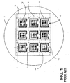
- FIG. 1 shows that the silicon wafer 9 contains only nine ICs 12, each silicon wafer 9 typically contains hundreds of ICs 12 arranged in rows and columns.
- Each IC 12 includes an array of pixels comprising IC electrodes 16 driven via corresponding switching elements 17.
- the other substrate is typically a glass wafer 10 that has thereon one transparent electrode 15 per corresponding IC 12.
- Each substrate is typically, but not necessarily, less than 1 mm thick; the thickness of each substrate may vary according to the manner in which the lcmds are to be used.
- a sealant that forms lcmd wall 11 is applied to one of the substrates.
- the wall 11 does not completely surround each IC 12 - a small gap 13 remains through which the liquid crystal material flows to fill the lcmds.
- the silicon wafer 9 is then aligned and joined with the glass wafer 10 such that the transparent electrodes 15 are aligned with the corresponding ICs 12.
- Spacers are used to keep the substrates separated by a small distance which is typically on the order of a few micrometers. The spacers may, for example, be etched onto the silicon wafer. After the substrates are joined, lcmds 8 are formed, each containing an IC 12.
- the lcmds 8 are filled with liquid crystal material via openings 13 after they are separated.
- the lcmds 8 may be separated from each other by using, for example, a scribe and break process.
- a scribe and break process the semiconductor wafer 9 is scribed (typically with a specialized saw or laser) along scribe lines 14, in order to weaken the locations where the separation is to take place.
- the glass wafer 10 is scribed using a cutting tool such as a laser or a specially designed saw.
- the wafers 9 & 10 are typically then temporarily glued onto a flexible material that is then flexed in order to break up the wafers and separate the lcmds.
- the scribe and break process results in small debris of semiconductor and glass material that accumulate around lcmd openings 13.
- the lcmds are filled with liquid crystal material.
- the filling is preferably achieved in a vacuum unit in which the lcmds are immersed in liquid crystal material.
- the hole 13 through which it is filled is then sealed with a glue or epoxy material.
- the traditional filling process described above often results in a large number of defective lcmds because debris from the scribe and break process are frequently pulled into many of the lcmds 8 by the in-flowing liquid crystal material.
- the debris may cause an electronic malfunction or may distort an image by blocking or altering the path of the electromagnetic radiation controlled by the lcmd.
- the defects caused by the debris are not discovered until after the lcmds are packaged since the packaging provides the wiring through which the lcmd receives imaging and testing signals.
- Packaging an lcmd involves mounting and wiring.
- the lcmd is mounted into/onto a packaging unit at a predetermined angle and location so that the image produced is properly focused and aligned.
- the lcmd is also wired to terminals on the packaging unit. These terminals will eventually be connected to and will receive imaging and other signals from a host device, such as, for example, a camera.
- the area surrounding the wiring connections is typically filled with a glue or epoxy material that stabilizes the connections and prevents the wires from touching each other.
- the lcmds are packaged, they are tested so that defective units may be detected and eliminated.
- the testing can be difficult and costly since each individual lcmd must be tested separately.
- the reason that the lcmds cannot be tested while they are still part of a substrate assembly is because the testing must take place after the liquid crystal filling process (which has traditionally needed to be performed after the separation of the lcmds 8 due to viscosity limitations).
- the packaging process is relatively expensive and may account for most of the cost of a finished lcmd. Packaging the lcmds prior to testing significantly increases the cost associated with defective units since such cost would also include the cost of packaging.
- a liquid crystal micro display (lcmd) is manufactured by creating a hole in an lcmd surface, filling the lcmd with liquid crystal material through the hole, and then sealing the hole.
- the invention allows an lcmd to be tested before it is separated from other lcmds and packaged. As a result, the invention increases the yield and reduces the cost associated with lcmd manufacturing.
- FIG. 3 depicts a flow chart illustrating a method of manufacturing lcmds of the present invention.
- Lcmds are formed using two substrates.
- the first substrate is a silicon wafer 21 (less than 1 mm thick) on which many (typically hundreds) of ICs are formed.
- Each IC 22 includes a large number (typically about half a million) of active pixels comprising electrodes 40 driven by corresponding switching elements 41.
- the thickness of each substrate may vary according to the application for which the lcmds will be used.
- the second substrate is transparent and is typically a thin glass wafer 26 having the transparent electrodes 42 of a corresponding number of lcmds.
- the transparent electrodes 42 are made from a transparent conductive material such as indium-tin oxide.
- Fill holes 33 are created in one of the wafers as indicated in step 3A.
- the fill holes 33 are carefully positioned so as to provide access to the chamber 35 of each lcmd 30 without damaging the ICs 22 or the display area of the lcmd 30.
- a fill hole 33 may be positioned as illustrated in FIGS. 4 and 5.
- the fill holes 33 may be created in either the glass wafer 26 or the silicon wafer 21. If the fill holes 33 are to be in the glass wafer 26, then they may be created using a glass drilling tool such as a laser device or a rotary drill. However, the fill holes 33 are preferably created in the silicon wafer 21 using an anisotropic etch.
- the anisotropic etch creates a funnel-shaped fill hole 33 in the silicon wafer 21 such that the opening in the inner surface of the silicon wafer 21 is smaller than the opening in the outer surface, as illustrated in FIG. 5.
- the anisotropic etch helps to more precisely place the fill holes 33 in the desired areas of the inner surface of the silicon wafer 21.
- step 3B This step typically involves applying a sealant material around each IC 22 and then joining the wafers to form lcmd units 30.
- the lcmd units 30 are then filled with liquid crystal material via the fill holes 33, as indicated in step 3C.
- the filling is preferably achieved using a standard vacuum filling technique whereby lcmds are placed in a vacuum chamber (not shown) in which air pressure is subsequently reduced; the lcmd units are then lowered into a bath of liquid crystal material and the pressure in the vacuum chamber is reasserted such that the pressure difference between the lcmd chambers 35 and their surroundings forces the liquid crystal material into the lcmd chambers 35 through the fill holes 33.
- Other filling methods may also be used, such as, for example, injecting or pouring the liquid crystal material into the lcmds through their respective fill holes 33.
- the lcmds are then tested as indicated in step 3E. Since the lcmds are still part of the same substrates and are still physically connected, they are easily handled during testing. Each row or column of lcmds may share the same testing signal(s) as illustrated in FIG. 4 and discussed in the related description below. Lcmds that appear to be defective are marked using, for example, an ink marker, so that they may be identified and disposed of at a later time. After the lcmds are tested, they are separated along scribe lines 36 (as indicated in step 3F) using, for example, a scribe and break process as discussed above. By following the above described steps, the debris caused by the scribe and break process should not affect the quality or performance of the lcmds since they are filled and sealed before debris are generated.
- steps 3A-3F may occur out of the order illustrated in FIG. 3.
- step 3B may occur before step 3A.
- each one of steps 3A-3F may comprise sub-steps.
- FIG. 4 is a top view of an example lcmd substrate assembly formed by the silicon wafer 21 and the glass wafer 26 before being divided into individual lcmds.
- the silicon wafer 21 is shown to contain only 9 ICs. Typically, however, such a silicon wafer would contain hundreds of ICs.
- Each IC, such as IC 22, is surrounded by a sealant wall 23 and is resistively connected to other ICs and to a testing terminal, such as testing terminal 25, located on the silicon wafer 21 and used for receiving a testing signal.
- a glass wafer 26 covers the ICs and is joined to the silicon wafer via the sealant walls 23 that surround the ICs.
- the glass wafer 26 is layered with typically one transparent electrode 42 (FIG.
- Transparent electrodes 42 are made from a transparent material such as indium-tin oxide. Parallel paths, such as paths 28 and 29 are used to reduce the impact of open circuits during testing.
- the glass wafer 26 is placed over the silicon wafer in such a way as to not cover the testing terminals on the silicon wafer.
- FIG. 5 is a cross sectional view of a simplified version an lcmd 30 of FIG. 4.
- Lcmd 30 contains an lcmd chamber 35 that is filled with liquid crystal material through fill hole 33.
- the filling is preferably performed in a vacuum chamber as discussed above.
- the fill hole 33 is sealed using a sealing object, such as a plug, or a sealing material such as glue, epoxy, or solder.
- the filling and testing processes of this invention are easier than the traditional filling and testing processes since lcmds do not have to be individually handled. Instead, lcmds 30 are filled and tested before they are separated. Furthermore, fewer defects are caused during the new filling process since no debris from the scribe and break process are pulled into the lcmds.
- FIG. 6 illustrates the testing of an lcmd in accordance with an embodiment of the present invention.
- very few pixel electrodes 40 and corresponding switching elements 41 are shown.
- each lcmd tested may contain hundreds of thousands or even millions of pixels.
- an electric signal is sent to one or more ICs 22 through a testing terminal, such as testing terminal 25 (FIG. 4).
- the testing signal is routed through a connection 54 to a switching element 53 that is fabricated in or forms part of the IC 22.
- Each connection, such as connections 54 and 56 may be resistive and/or may incorporate a resistive element.
- the testing signal causes the switching element 53 to connect the pixel electrodes 40 to a grounding terminal 52 via respective switching elements 41.
- the grounding terminal 52 may be located on the silicon wafer and may be grounded through a connection that is routed between scribe lines.
- a corresponding transparent electrode 42 (FIG. 5) on the glass wafer 26 may be driven with varying voltages to create an all "black”, an all “white”, and/or an intermediate gray display.
- Optical testing equipment such as, for example, a specialized camera, can then be used to evaluate the lcmd's performance in response to the testing signals. The optical testing equipment tests to see if the lcmd produces a non-uniform image. An lcmd image may be non-uniform for various reasons such as, for example, the presence of debris in the lcmd or incomplete liquid crystal filling.
- An lcmd that produces a non-uniform image can be marked using, for example, an ink marker, so that it can be disposed of after the lcmds are separated.
- an ink marker for example, an ink marker
Landscapes
- Physics & Mathematics (AREA)
- Nonlinear Science (AREA)
- Chemical & Material Sciences (AREA)
- Crystallography & Structural Chemistry (AREA)
- General Physics & Mathematics (AREA)
- Optics & Photonics (AREA)
- Mathematical Physics (AREA)
- Engineering & Computer Science (AREA)
- Manufacturing & Machinery (AREA)
- Liquid Crystal (AREA)
Abstract
Description
Claims (18)
- A method of manufacturing a liquid crystal micro display (lcmd), said method comprising:creating a hole in a substrate;causing liquid crystal material to flow through said hole; andsealing said hole.
- The method of claim 1, further comprising :testing said lcmd after sealing said hole.
- The method of claim 2, further comprising:separating said lcmd from other lcmds after testing said lcmd.
- The method of one of the preceding claims, wherein said substrate is a semiconductor substrate.
- The method of claim 4, wherein the semiconductor substrate comprises an integrated circuit.
- The method of claim 4 or 5, wherein the semiconductor substrate is part of a silicon wafer.
- The method of claim 1, wherein said substrate comprises glass.
- The method of one of the preceding claims, wherein said hole is sealed using a sealant material selected from a group consisting of glue, epoxy, and solder.
- A method of manufacturing a first liquid crystal micro display (lcmd) comprising:testing said first lcmd while it is physically connected to a second lcmd; andseparating said first lcmd from said second lcmd after said testing.
- The method of claim 9, wherein said first lcmd comprises a semiconductor substrate having an integrated circuit and a glass substrate having a transparent electrode.
- The method of claim 10, wherein said integrated circuit comprises electrodes.
- The method of claim 11, wherein said testing includes causing a voltage difference between the integrated circuit electrodes and the transparent electrode.
- The method of claim 12, wherein said testing includes determining whether the lcmd produces a uniform image.
- A liquid crystal micro display (lcmd) comprising:a first substrate; anda second substrate having a hole extending through a thickness thereof.
- The lcmd of claim 14, wherein said hole can be used for filling the lcmd with liquid crystal material.
- The lcmd of claim 14 or 15, wherein the second substrate is a semiconductor substrate comprising an integrated circuit.
- The lcmd of claim 14 or 15, wherein the second substrate comprises glass.
- The lcmd of one of claims 14 to 17, wherein said lcmd is physically connected to other lcmds.
Priority Applications (1)
| Application Number | Priority Date | Filing Date | Title |
|---|---|---|---|
| EP06007058A EP1674921A3 (en) | 2001-04-25 | 2002-01-17 | System and method for manufacturing liquid crystal micro displays |
Applications Claiming Priority (2)
| Application Number | Priority Date | Filing Date | Title |
|---|---|---|---|
| US842100 | 2001-04-25 | ||
| US09/842,100 US6750939B2 (en) | 2001-04-25 | 2001-04-25 | System and method for manufacturing liquid crystal micro displays |
Related Child Applications (1)
| Application Number | Title | Priority Date | Filing Date |
|---|---|---|---|
| EP06007058A Division EP1674921A3 (en) | 2001-04-25 | 2002-01-17 | System and method for manufacturing liquid crystal micro displays |
Publications (3)
| Publication Number | Publication Date |
|---|---|
| EP1253460A2 true EP1253460A2 (en) | 2002-10-30 |
| EP1253460A3 EP1253460A3 (en) | 2003-10-22 |
| EP1253460B1 EP1253460B1 (en) | 2006-04-05 |
Family
ID=25286525
Family Applications (2)
| Application Number | Title | Priority Date | Filing Date |
|---|---|---|---|
| EP06007058A Withdrawn EP1674921A3 (en) | 2001-04-25 | 2002-01-17 | System and method for manufacturing liquid crystal micro displays |
| EP02001248A Expired - Lifetime EP1253460B1 (en) | 2001-04-25 | 2002-01-17 | System and method for manufacturing liquid crystal micro displays |
Family Applications Before (1)
| Application Number | Title | Priority Date | Filing Date |
|---|---|---|---|
| EP06007058A Withdrawn EP1674921A3 (en) | 2001-04-25 | 2002-01-17 | System and method for manufacturing liquid crystal micro displays |
Country Status (4)
| Country | Link |
|---|---|
| US (1) | US6750939B2 (en) |
| EP (2) | EP1674921A3 (en) |
| JP (1) | JP2003005202A (en) |
| DE (1) | DE60210361T2 (en) |
Cited By (2)
| Publication number | Priority date | Publication date | Assignee | Title |
|---|---|---|---|---|
| EP1662304A4 (en) * | 2003-09-04 | 2007-11-07 | Fujitsu Ltd | DISPLAY DEVICE, METHOD FOR CONTROLLING THE SAME, AND PORTABLE DISPLAY DEVICE |
| US7760837B2 (en) | 2006-01-10 | 2010-07-20 | Fujitsu Semiconductor Limited | Synchronization determination method and apparatus |
Families Citing this family (12)
| Publication number | Priority date | Publication date | Assignee | Title |
|---|---|---|---|---|
| US6809337B2 (en) * | 2002-04-22 | 2004-10-26 | Intel Corporation | Liquid crystal display devices having fill holes and electrical contacts on the back side of the die |
| US6891592B2 (en) * | 2002-07-26 | 2005-05-10 | Intel Corporation | Wafer level electro-optical sort testing and wafer level assembly of micro liquid crystal-on silicon (LCOS) devices |
| US20050122464A1 (en) * | 2003-12-03 | 2005-06-09 | International Business Machines Corporation | One-drop fill spacerless process for liquid crystal cell on a silicon backplane or microdisplays |
| US7938051B2 (en) * | 2004-05-21 | 2011-05-10 | Tannas Lawrence E | Apparatus and methods for cutting electronic displays during resizing |
| US7692757B2 (en) * | 2004-07-30 | 2010-04-06 | Intel Corporation | Wafer scale fabrication of liquid crystal on silicon light modulation devices |
| JP2006100763A (en) * | 2004-09-06 | 2006-04-13 | Fuji Photo Film Co Ltd | Solid-state imaging device manufacturing method and joining device |
| JP4854728B2 (en) * | 2006-03-07 | 2012-01-18 | 富士通株式会社 | Method and apparatus for manufacturing liquid crystal display panel |
| DE102006032047A1 (en) * | 2006-07-10 | 2008-01-24 | Schott Ag | Optoelectronic component e.g. image signal-detecting component, manufacturing method for e.g. digital fixed image camera, involves positioning components either one by one or in groups relative to position of associated components of wafer |
| US7786747B2 (en) * | 2007-11-30 | 2010-08-31 | Texas Instruments Incorporated | Microdisplay assemblies and methods of packaging microdisplays |
| WO2011050455A1 (en) | 2009-10-27 | 2011-05-05 | Lensvector Inc. | Method and apparatus for testing operation of an optical liquid crystal device, and manufacturing of device |
| JP6672832B2 (en) * | 2016-01-26 | 2020-03-25 | ソニー株式会社 | Liquid crystal display and electronic equipment |
| KR102962540B1 (en) * | 2023-03-31 | 2026-05-07 | 젠텍스 코포레이션 | Electro-optical device having barrier properties |
Family Cites Families (19)
| Publication number | Priority date | Publication date | Assignee | Title |
|---|---|---|---|---|
| JPS56128919A (en) * | 1980-03-14 | 1981-10-08 | Matsushita Electric Ind Co Ltd | Manufacture of picture display panel |
| JPS61217018A (en) * | 1985-03-23 | 1986-09-26 | Sharp Corp | Manufacture of liquid-crystal display element |
| JPH02222925A (en) * | 1988-11-07 | 1990-09-05 | Matsushita Electric Ind Co Ltd | Production of liquid crystal panel |
| JP2834935B2 (en) * | 1992-06-11 | 1998-12-14 | シャープ株式会社 | Active matrix display element and method of manufacturing the same |
| KR100445816B1 (en) * | 1995-11-02 | 2004-11-09 | 세이코 엡슨 가부시키가이샤 | Liquid crystal panel manufacturing method |
| JPH10260415A (en) * | 1997-03-19 | 1998-09-29 | Shimadzu Corp | Liquid crystal injection device |
| US6122033A (en) * | 1998-04-06 | 2000-09-19 | National Semiconductor Corporation | Fusible seal for LCD devices and methods for making same |
| EP0962803A1 (en) * | 1998-06-08 | 1999-12-08 | Asulab S.A. | Method of batch manufacturing of electro-optical cells or of electro-chemical photovoltaic cells |
| US6177288B1 (en) * | 1998-06-19 | 2001-01-23 | National Semiconductor Corporation | Method of making integrated circuit packages |
| JP3481465B2 (en) * | 1998-07-14 | 2003-12-22 | シャープ株式会社 | Aggregated substrate of active matrix substrate |
| US6005649A (en) * | 1998-07-22 | 1999-12-21 | Rainbow Displays, Inc. | Tiled, flat-panel microdisplay array having visually imperceptible seams |
| JP2000206545A (en) * | 1999-01-13 | 2000-07-28 | Ran Technical Service Kk | Liquid crystal sealing device |
| US6555408B1 (en) * | 1999-02-05 | 2003-04-29 | Alien Technology Corporation | Methods for transferring elements from a template to a substrate |
| US6556261B1 (en) * | 1999-02-15 | 2003-04-29 | Rainbow Displays, Inc. | Method for assembling a tiled, flat-panel microdisplay array having reflective microdisplay tiles and attaching thermally-conductive substrate |
| US6476886B2 (en) * | 1999-02-15 | 2002-11-05 | Rainbow Displays, Inc. | Method for assembling a tiled, flat-panel microdisplay array |
| US6275277B1 (en) * | 1999-05-17 | 2001-08-14 | Colorado Microdisplay, Inc. | Micro liquid crystal displays having a circular cover glass and a viewing area free of spacers |
| US6721029B2 (en) * | 1999-08-23 | 2004-04-13 | Agilent Technologies, Inc. | Electro-optical material-based display device |
| US6562640B1 (en) * | 2000-08-23 | 2003-05-13 | Taiwan Micro Display Corporation | Method of manufacturing micro-display |
| KR100643562B1 (en) * | 2000-11-28 | 2006-11-10 | 엘지.필립스 엘시디 주식회사 | Manufacturing process of liquid crystal cell for small liquid crystal display device |
-
2001
- 2001-04-25 US US09/842,100 patent/US6750939B2/en not_active Expired - Lifetime
-
2002
- 2002-01-17 EP EP06007058A patent/EP1674921A3/en not_active Withdrawn
- 2002-01-17 DE DE60210361T patent/DE60210361T2/en not_active Expired - Fee Related
- 2002-01-17 EP EP02001248A patent/EP1253460B1/en not_active Expired - Lifetime
- 2002-04-10 JP JP2002107797A patent/JP2003005202A/en active Pending
Cited By (3)
| Publication number | Priority date | Publication date | Assignee | Title |
|---|---|---|---|---|
| EP1662304A4 (en) * | 2003-09-04 | 2007-11-07 | Fujitsu Ltd | DISPLAY DEVICE, METHOD FOR CONTROLLING THE SAME, AND PORTABLE DISPLAY DEVICE |
| EP2278390A1 (en) * | 2003-09-04 | 2011-01-26 | Fujitsu Limited | Display element having wall structure, method of driving the display element and non-contact IC card as portable display device using the display element |
| US7760837B2 (en) | 2006-01-10 | 2010-07-20 | Fujitsu Semiconductor Limited | Synchronization determination method and apparatus |
Also Published As
| Publication number | Publication date |
|---|---|
| US20020159020A1 (en) | 2002-10-31 |
| EP1674921A3 (en) | 2008-10-15 |
| EP1674921A2 (en) | 2006-06-28 |
| JP2003005202A (en) | 2003-01-08 |
| US6750939B2 (en) | 2004-06-15 |
| EP1253460A3 (en) | 2003-10-22 |
| DE60210361T2 (en) | 2007-03-15 |
| DE60210361D1 (en) | 2006-05-18 |
| EP1253460B1 (en) | 2006-04-05 |
Similar Documents
| Publication | Publication Date | Title |
|---|---|---|
| US6750939B2 (en) | System and method for manufacturing liquid crystal micro displays | |
| US8507297B2 (en) | Packaging and testing of multiple MEMS devices on a wafer | |
| US4897708A (en) | Semiconductor wafer array | |
| US6891592B2 (en) | Wafer level electro-optical sort testing and wafer level assembly of micro liquid crystal-on silicon (LCOS) devices | |
| CA1301370C (en) | Integrated circuit package using plastic encapsulant | |
| US6908791B2 (en) | MEMS device wafer-level package | |
| US20060148137A1 (en) | Integrated MEMS packaging | |
| US20020048924A1 (en) | Metal bump with an insulating sidewall and method of fabricating thereof | |
| US20050236696A1 (en) | Fan out type wafer level package structure and method of the same | |
| JPH10221695A (en) | Liquid crystal display and its manufacturing process | |
| CN101221330A (en) | Liquid crystal display device | |
| CN100521217C (en) | Optical device | |
| US6809337B2 (en) | Liquid crystal display devices having fill holes and electrical contacts on the back side of the die | |
| KR20130040573A (en) | Display device | |
| KR20200086918A (en) | Integrated circuit chip, integrated circuit package and display apparatus including integrated circuit chip | |
| JP2006501641A (en) | Optical microsystem and method for forming the same | |
| KR20020094636A (en) | Fabricating method of liquid crystal display | |
| US7692757B2 (en) | Wafer scale fabrication of liquid crystal on silicon light modulation devices | |
| EP0267688A1 (en) | Improvements relating to liquid crystal devices | |
| US20180130846A1 (en) | Semiconductor device | |
| CN100524637C (en) | Method for wafer level packaging of optical devices using scribe and break processes | |
| JPH05341246A (en) | Manufacture of matrix type display element | |
| CN100524670C (en) | Method for manufacturing organic light emitting display | |
| JPH08234215A (en) | Liquid crystal display | |
| CN115777069A (en) | Inspection cartridge |
Legal Events
| Date | Code | Title | Description |
|---|---|---|---|
| PUAI | Public reference made under article 153(3) epc to a published international application that has entered the european phase |
Free format text: ORIGINAL CODE: 0009012 |
|
| AK | Designated contracting states |
Kind code of ref document: A2 Designated state(s): AT BE CH CY DE DK ES FI FR GB GR IE IT LI LU MC NL PT SE TR |
|
| AX | Request for extension of the european patent |
Free format text: AL;LT;LV;MK;RO;SI |
|
| RIC1 | Information provided on ipc code assigned before grant |
Ipc: 7G 02F 1/1333 B Ipc: 7G 02F 1/1362 B Ipc: 7G 02F 1/1341 A |
|
| PUAL | Search report despatched |
Free format text: ORIGINAL CODE: 0009013 |
|
| AK | Designated contracting states |
Kind code of ref document: A3 Designated state(s): AT BE CH CY DE DK ES FI FR GB GR IE IT LI LU MC NL PT SE TR |
|
| AX | Request for extension of the european patent |
Extension state: AL LT LV MK RO SI |
|
| 17P | Request for examination filed |
Effective date: 20040323 |
|
| AKX | Designation fees paid |
Designated state(s): DE FR GB |
|
| 17Q | First examination report despatched |
Effective date: 20050412 |
|
| GRAP | Despatch of communication of intention to grant a patent |
Free format text: ORIGINAL CODE: EPIDOSNIGR1 |
|
| GRAS | Grant fee paid |
Free format text: ORIGINAL CODE: EPIDOSNIGR3 |
|
| GRAA | (expected) grant |
Free format text: ORIGINAL CODE: 0009210 |
|
| AK | Designated contracting states |
Kind code of ref document: B1 Designated state(s): DE FR GB |
|
| REG | Reference to a national code |
Ref country code: GB Ref legal event code: FG4D |
|
| REF | Corresponds to: |
Ref document number: 60210361 Country of ref document: DE Date of ref document: 20060518 Kind code of ref document: P |
|
| REG | Reference to a national code |
Ref country code: GB Ref legal event code: 732E |
|
| ET | Fr: translation filed | ||
| RAP2 | Party data changed (patent owner data changed or rights of a patent transferred) |
Owner name: AVAGO TECHNOLOGIES ECBU IP (SINGAPORE) PTE. LTD. |
|
| PLBE | No opposition filed within time limit |
Free format text: ORIGINAL CODE: 0009261 |
|
| STAA | Information on the status of an ep patent application or granted ep patent |
Free format text: STATUS: NO OPPOSITION FILED WITHIN TIME LIMIT |
|
| 26N | No opposition filed |
Effective date: 20070108 |
|
| PGFP | Annual fee paid to national office [announced via postgrant information from national office to epo] |
Ref country code: FR Payment date: 20070117 Year of fee payment: 6 |
|
| REG | Reference to a national code |
Ref country code: FR Ref legal event code: ST Effective date: 20081029 |
|
| PG25 | Lapsed in a contracting state [announced via postgrant information from national office to epo] |
Ref country code: FR Free format text: LAPSE BECAUSE OF NON-PAYMENT OF DUE FEES Effective date: 20080131 |
|
| PGFP | Annual fee paid to national office [announced via postgrant information from national office to epo] |
Ref country code: DE Payment date: 20090115 Year of fee payment: 8 |
|
| PG25 | Lapsed in a contracting state [announced via postgrant information from national office to epo] |
Ref country code: DE Free format text: LAPSE BECAUSE OF NON-PAYMENT OF DUE FEES Effective date: 20100803 |
|
| REG | Reference to a national code |
Ref country code: GB Ref legal event code: 732E Free format text: REGISTERED BETWEEN 20111201 AND 20111207 |
|
| PGFP | Annual fee paid to national office [announced via postgrant information from national office to epo] |
Ref country code: GB Payment date: 20201102 Year of fee payment: 20 |
|
| REG | Reference to a national code |
Ref country code: GB Ref legal event code: PE20 Expiry date: 20220116 |
|
| PG25 | Lapsed in a contracting state [announced via postgrant information from national office to epo] |
Ref country code: GB Free format text: LAPSE BECAUSE OF EXPIRATION OF PROTECTION Effective date: 20220116 |