EP1253442A1 - X-ray image sensor - Google Patents
X-ray image sensor Download PDFInfo
- Publication number
- EP1253442A1 EP1253442A1 EP01900661A EP01900661A EP1253442A1 EP 1253442 A1 EP1253442 A1 EP 1253442A1 EP 01900661 A EP01900661 A EP 01900661A EP 01900661 A EP01900661 A EP 01900661A EP 1253442 A1 EP1253442 A1 EP 1253442A1
- Authority
- EP
- European Patent Office
- Prior art keywords
- substrate
- scintillator
- imaging device
- state imaging
- solid
- Prior art date
- Legal status (The legal status is an assumption and is not a legal conclusion. Google has not performed a legal analysis and makes no representation as to the accuracy of the status listed.)
- Granted
Links
Images


Classifications
-
- G—PHYSICS
- G01—MEASURING; TESTING
- G01T—MEASUREMENT OF NUCLEAR OR X-RADIATION
- G01T1/00—Measuring X-radiation, gamma radiation, corpuscular radiation, or cosmic radiation
- G01T1/16—Measuring radiation intensity
- G01T1/20—Measuring radiation intensity with scintillation detectors
- G01T1/2018—Scintillation-photodiode combinations
- G01T1/20188—Auxiliary details, e.g. casings or cooling
-
- G—PHYSICS
- G01—MEASURING; TESTING
- G01T—MEASUREMENT OF NUCLEAR OR X-RADIATION
- G01T1/00—Measuring X-radiation, gamma radiation, corpuscular radiation, or cosmic radiation
- G01T1/16—Measuring radiation intensity
- G01T1/20—Measuring radiation intensity with scintillation detectors
- G01T1/2018—Scintillation-photodiode combinations
- G01T1/20188—Auxiliary details, e.g. casings or cooling
- G01T1/2019—Shielding against direct hits
Definitions
- the present invention relates to an X-ray image detection apparatus.
- this X-ray image detection apparatus comprises a scintillator substrate having a scintillator evaporated on an X-ray-transparent substrate; a solid-state imaging device having an imaging plane on which the scintillator is disposed; a mount substrate, formed with a lead for inputting an output signal from the solid-state imaging device, for securing the solid-state imaging device; a frame, secured onto the mount substrate so as to surround the solid-state imaging device, having a positioning portion projecting toward the scintillator substrate such that at least a part thereof abuts against the scintillator substrate; and a bonding wire, positioned within a space between the positioning portion and the mount substrate, for connecting the solid-state imaging device and the lead to each other.
- An X-ray image transmitted through the X-ray-transparent substrate is converted by the scintillator formed thereon into a visible image.
- This visible image is made directly incident on the imaging plane of the solid-state imaging device, whereas video signals of the visible image outputted from the solid-state imaging device are outputted to the lead formed on the mount substrate by way of the bonding wire protected by the positioning portion. Therefore, X-ray images with a favorable quality can be obtained in this apparatus.
- the positioning portion of the frame protects the bonding wire positioned thereunder while positioning and supporting the scintillator substrate abutting thereagainst, whereby it is not necessary for the solid-state imaging device to be bonded with an adhesive which may incorporate bubbles therein.
- the frame is made of a metal, it improves a shield effect for restraining X-rays from entering the readout section of the solid-state imaging device, bonding wires, bonding pads, and the like.
- the positioning portion of the frame be further provided with a shield member made of an X-ray-shielding material on a side opposite from the bonding wire, so as to block the X-rays.
- the scintillator substrate will be positioned if two sides of the periphery of the scintillator substrate are pressed against two inner sides of the positioning portion in cases where the inside of the positioning portion is rectangular (e.g., square) while the periphery of the scintillator substrate is rectangular (e.g., square), whereby it is not necessary for both of them to be in contact with each other at all of the four sides.
- the apparatus further comprise a press plate secured to the frame so as to close an opening of the frame, and an elastic body interposed between the press plate and the scintillator substrate, the elastic body pressing the scintillator substrate toward the solid-state imaging device.
- the scintillator substrate is pressed toward the solid-state imaging device while being secured by the press plate and the elastic body, so as to contact the scintillator substrate with the solid-state imaging device, whereby X-ray images with a better quality can be obtained.
- the substrate is set relatively thin in order to improve the X-ray transmissivity of the X-ray-transparent substrate even slightly.
- the substrate may be bent, thereby deteriorating images. Since the contact is enhanced by pressing in the apparatus as mentioned above, the bent of the substrate is corrected, whereby images with a better quality can be obtained.
- the contact of the scintillator substrate and the solid-state imaging device can be improved when the apparatus comprises a press plated secured to the frame so as to close the opening of the frame whereas the thickness of the scintillator substrate is set such that the X-ray-transparent substrate comes into contact with the press plate, whereby images with a favorable quality can be obtained as in the above.
- the positioning portion and the scintillator substrate be bonded together.
- the bonding further enhances the positioning of the scintillator substrate, and makes it unnecessary to use an adhesive between the scintillator substrate and the imaging plane of the solid-state imaging device, whereby shadows due to bubbles can be prevented.
- Such a bonding technique can also be carried out without using a press plate, so that the surface of the X-ray-transparent substrate on the side opposite from the scintillator can be exposed as well. This can improve the X-ray incidence to the scintillator.
- the scintillator be coated with a resin film.
- the resin film may be either a single layer or multilayer. When it is a single layer, it can suppress the attenuation factor of visible light images generated in the scintillator. When compared with the multilayer coating, however, its moisture resistance is inferior.
- the adhesive applied to the positioning portion also exhibits a moisture-proofing effect in the space where the scintillator is installed, whereby the use of a single layer coating of resin film not only suppresses the attenuation factor of visible light images but also improves the moisture resistance.
- the X-ray-transparent substrate is made of X-ray-transparent glass or amorphous carbon
- the scintillator is made of CsI having a columnar crystal
- the resin film is made of polyparaxylylene.
- the solid-state imaging device be constituted by a plurality of semiconductor imaging device chips. While the bubbles may be remarkably formed when the imaging plane is coated with an adhesive as conventionally effected in such a case, the apparatus can securely restrain this phenomenon from occurring.
- Fig. 1 is a vertical sectional view of the X-ray image detection apparatus in accordance with the first embodiment.
- This apparatus comprises a scintillator substrate 1 having a scintillator 1b on a surface of an X-ray-transparent substrate 1a.
- this apparatus comprises a solid-state imaging device 2 having an imaging plane on which the scintillator 1b is disposed. The scintillator 1b is in contact with the imaging plane. When the scintillator 1b is coated with a resin film, the latter comes into contact with the imaging plane.
- the solid-state imaging device 2 may be constituted by a CCD image sensor, it is a MOS type image sensor in this example.
- the solid-state imaging device 2 is secured onto the mount substrate 3.
- the surface of the mount substrate 3 is formed with a lead 3a for inputting output signals from the solid-state imaging device 2.
- the apparatus further comprises a frame 4 secured onto the mount substrate 3 so as to surround the solid-state imaging device 2 .
- the frame 4 has a positioning portion 4a projecting toward the scintillator substrate 1 so as to abut against the scintillator substrate 1.
- the scintillator substrate 1 has a rectangular or square form.
- the positioning portion 4a surrounds four side faces of the scintillator substrate 1, so as to come into contact therewith.
- the scintillator substrate 1 will be positioned if two sides of the periphery of the scintillator substrate 1 are pressed against two inner sides of the positioning portion 4a in cases where inside periphery of the positioning portion 4a is rectangular (e.g., square) while the periphery of the scintillator substrate 1 is rectangular (e.g., square), whereby it is not necessary for both of them to be in contact with each other at all of four sides.
- a space S is formed between the positioning portion 4a and the mount substrate 3. Positioned within the space S are a readout section of the solid-state imaging device 2, a bonding pad portion connecting with the lead 3a on the mount 3, and a bonding wire 5 for connecting the solid-state imaging device 2 and the lead 3a to each other.
- a connector 6 for inputting driving signals for driving the solid-state imaging device 2 and reading out output signals is attached to the mount substrate 3 on the back side.
- X-rays are incident on the scintillator 1b in a direction through the X-ray-transparent substrate 1a.
- An X-ray image transmitted through the X-ray-transparent substrate 1a is converted by the scintillator 1b formed thereon into a visible image, which is directly incident on the imaging plane of the solid-state imaging device 2, whereas video signals of the visible image outputted from the solid-state imaging device 2 are fed into the lead 3a formed on the mount substrate 3 by way of the bonding wire 5 protected by the positioning portion 4a.
- a driving circuit for driving the solid-state imaging device 2, and an amplifier for receiving a video signal outputted from the solid-state imaging device 3 by way of the lead 3a and amplifying thus received video signal.
- This video signal is outputted as an X-ray image from the connector 6.
- the positioning portion 4a of the frame 4 protects the bonding wire 5 positioned thereunder, while positioning and supporting the scintillator substrate 1 in contact therewith, whereby it is not necessary for the solid-state imaging device 2 to be bonded with an adhesive which may incorporate bubbles therein.
- the frame 4 is made of a metal, it improves a shield effect for restraining the X-rays from entering the readout section of the solid-state imaging device 2, the bonding wire 5, bonding pads, and the like.
- the positioning portion 4a of the frame 4 is further provided with a shield member 7 made of an X-ray-shielding material on a side opposite from the bonding wire 5, so as to fully block the X-rays.
- the shield member 7 is made of lead.
- the scintillator substrate 1 is secured to the mount substrate 3.
- the apparatus comprises a press plate 8 secured to the frame 4 so as to close the opening of the frame 4, and an elastic body 9 interposed between the press plate 8 and the scintillator substrate 1, whereas the elastic body 9 presses the scintillator substrate 1 toward the solid-state imaging device 2.
- the elastic body is constituted by a sponge made of urethane or the like.
- the scintillator substrate 1 is pressed toward the solid-state imaging device 2 while being secured to the mount substrate 3 by the press plate 8 and the elastic body 9, whereby the contact of the scintillator substrate 1 to the solid-state imaging device 2 can be enhanced, so as to yield X-ray images with abetter quality.
- the substrate 1a is set relatively thin when incident X-rays are soft X-rays in order to improve the X-ray transmissivity of the X-ray-transparent substrate, the substrate 1a may be bent when the substrate 1a is thin, thereby causing images to deteriorate. Since the contact is enhanced by pressing as mentioned above, the apparatus can correct the bent of the substrate, thereby yielding images with a better quality.
- the positioning portion 4a and the scintillator substrate 1 are bonded to each other with an adhesive 10.
- the bonding further strengthens the positioning of the scintillator substrate 1, and makes it unnecessary to use the adhesive between the scintillator substrate 1 and the imaging plane of the solid-state imaging device 2, whereby shadows due to bubbles can be prevented.
- the scintillator 1b is coated with a resin film 1c.
- the resin film 1c may be either a single layer or multilayer. When it is a single layer, it can suppress the attenuation factor of visible light images generated in the scintillator 1b. When compared with the multilayer coating, however, the single layer is inferior in the moisture resistance.
- the adhesive 10 applied to the positioning portion 4a also exhibits a moisture-proofing effect in the space where the scintillator is installed, whereby the use of a single layer coating of resin film not only suppresses the attenuation factor of visible light images but also improves the moisture resistance.
- the X-ray-transparent substrate 1a is made of X-ray-transparent glass or amorphous carbon
- the scintillator 1b is made of CsI having a columnar crystal
- the resin film is made of polyparaxylylene, so that a visible light image with a high resolution can be obtained while improving the transmissivity of X-rays, and this visible light image can be made incident on the solid-state imaging device 2 with a low attenuation factor.
- the shieldmember 7 also constitutes a positioning portion, whereas the upper face of the scintillator substrate 1 is set lower than the upper face of the positioning portion 4a of the frame 4.
- a positioning portion 4b for positioning the press plate is provided at the opening end of the frame 4. While the press plate 8 fits in the step of the positioning portion 4b, the lower face of the press plate 8 abuts against the upper faces of the shield member 7 and the positioning portion 4a on the right side in the drawing, whereas the press plate 8 is secured to the frame 4 with an adhesive interposed therebetween.
- Fig. 2 is a vertical sectional view of the X-ray image detection apparatus in accordance with the second embodiment.
- the configuration of this example is identical to that of the first embodiment except that the elastic body 9 used in the apparatus of the first embodiment is not provided.
- the thickness of the scintillator substrate 1 is set such that the X-ray-transparent substrate 1a comes into contact with the press plate 8, thereby improving the adhesion of the scintillator substrate 1 to the solid-state imaging device 2. Images having a favorable quality can also be obtained in this case as in the case mentioned above.
- the shield member 7 also constitutes a positioning portion, whereas the upper face of the positioning portion 4a of the frame 4 is located as high as the upper face of the scintillator substrate 1.
- Fig. 3 is a vertical sectional view of the X-ray image detection apparatus in accordance with the third embodiment.
- This example has a configuration identical to that of the second embodiment except that the press plate 8 in the second embodiment is omitted by using the above-mentioned adhesive 10. Namely, the surface of the X-ray-transparent substrate 1a on the side opposite from the scintillator 1b is exposed. Since the press plate 8 is omitted, the X-ray incidence rate to the scintillator 1b can be improved as compared with that in the second embodiment.
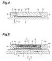
- Fig. 4 is a vertical sectional view of the X-ray image detection apparatus in accordance with the fourth embodiment.
- This example has a configuration identical to that of the third embodiment except that the upper face of the scintillator substrate 1 is set higher than the upper face of the positioning portion 4a of the frame 4. Since the substrate 1a proprudes slightly above the positioning portion 4a in this example, the scintillator substrate 1 can be inserted into the opening of the frame 4 while keeping the projecting part during the manufacture.
- Fig. 5 is a vertical sectional view of the X-ray image detection apparatus in accordance with the fifth embodiment.
- the solid-state imaging device 2 is not constituted by a single semiconductor solid-state imaging device chip, but a plurality of semiconductor solid-state imaging device chips 2' arranged adjacent each other into a plane. Except for this point, the apparatus has a configuration identical to that of the first embodiment.
- the bubbles may be remarkably formed if the imaging plane is coated with an adhesive as conventionally effected. The apparatus can securely restrain this phenomenon from occurring.
- a plurality of semiconductor solid-state imaging device chips 2' are pressed toward the mount substrate 3 by a mass of elastic body 9 such that all the imaging planes of the semiconductor solid-state imaging device chips 2' are positioned within the same plane, whereby the effect mentioned above is made remarkable, and the distortion of captured images can be reduced.
- the solid-state imaging device 2 constituted by a plurality of semiconductor solid-state imaging device chips 2' can also be employed in the apparatus of the second to fourth embodiments.
- Fig. 6 is a perspective view showing the X-ray image detection apparatus in accordance with a sixth embodiment in an exploded state.
- one of the X-ray image detection apparatus in accordance with the first to fifth embodiments is accommodated in a housing.
- This housing comprises a housing body HS L and an upper lid HS U adapted to mate therewith.
- the upper lid HS U is formed with an X-ray entrance opening OP.
- This opening OP is closed with an X-ray-transparent flat sheet 11 attached to the inside of the upper lid HS U , which is preferably made of polycarbonate or amorphous carbon.
- an electronic circuit unit 12 including driving circuits for driving the solid-state imaging device 2, an amplifier for amplifying video signals from the solid-state imaging device 2, and the like is provided on the back side of the mount substrate 3, whereas the power supply to these driving circuits, and the transmitting/receiving of control signals, video signals, and the like are carried out by way of a plurality of connectors provided in a side face of the housing.
- Spacers and stays ST are interposed between the mount substrate 3 and the bottom face of the housing, so as to secure a space in which the electronic circuit unit 12 is disposed. Since the devices are accommodated in the housing, this apparatus protects the electronic circuit unit 12 and the like.
- the present invention can be utilized in X-ray image detection apparatus.
Landscapes
- Physics & Mathematics (AREA)
- Health & Medical Sciences (AREA)
- Life Sciences & Earth Sciences (AREA)
- General Physics & Mathematics (AREA)
- High Energy & Nuclear Physics (AREA)
- Molecular Biology (AREA)
- Spectroscopy & Molecular Physics (AREA)
- Measurement Of Radiation (AREA)
- Solid State Image Pick-Up Elements (AREA)
- Transforming Light Signals Into Electric Signals (AREA)
Abstract
Description
Claims (11)
- An X-ray image detection apparatus comprising:a scintillator substrate having a scintillator formed on an X-ray-transparent substrate;a solid-state imaging device having an imaging plane on which said scintillator is disposed;a mount substrate, formed with a lead for inputting an output signal from said solid-state imaging device, for securing said solid-state imaging device;a frame, secured onto said mount substrate so as to surround said solid-state imaging device, having a positioning portion projecting toward said scintillator substrate such that at least a part thereof abuts against said scintillator substrate; anda bonding wire, positioned within a space between said positioning portion and said mount substrate, for connecting said solid-state imaging device and said lead to each other.
- An X-ray image detection apparatus according to claim 1, wherein said frame is made of a metal.
- An X-ray image detection apparatus according to claim 1, wherein said positioning portion of said frame is further provided with a shield member made of an X-ray-shielding material on a side opposite from said bonding wire.
- An X-ray image detection apparatus according to claim 1, further comprising a press plate secured to said frame so as to close an opening of said frame, and an elastic body interposed between said press plate and said scintillator substrate, said elastic body pressing said scintillator substrate toward said solid-state imaging device.
- An X-ray image detection apparatus according to claim 1, further comprising a press plate secured to said frame so as to close an opening of said frame, said scintillator substrate having a thickness set such that said X-ray-transparent substrate comes into contact with said press plate.
- An X-ray image detection apparatus according to claim 1, wherein said positioning portion and said scintillator substrate are bonded to each other.
- An X-ray image detection apparatus according to claim 6, wherein said X-ray-transparent substrate has an exposed surface on a side opposite from said scintillator.
- An X-ray image detection apparatus according to claim 1, wherein said scintillator is coated with a resin film.
- An X-ray image detection apparatus according to claim 8, wherein said X-ray-transparent substrate is made of X-ray-transparent glass or amorphous carbon, said scintillator is made of CsI having a columnar crystal, and said resin film is made of polyparaxylylene.
- An X-ray image detection apparatus according to claim 1, wherein said solid-state imaging device comprises a plurality of semiconductor solid-state imaging device chips arranged.
- An X-ray image detection apparatus according to claim 10, wherein said plurality of semiconductor solid-state imaging device chips are pressed toward said mount substrate by a mass of elastic body such that all the imaging planes of said plurality of semiconductor solid-state imaging device chips are positioned within a single plane.
Applications Claiming Priority (3)
| Application Number | Priority Date | Filing Date | Title |
|---|---|---|---|
| JP2000002900 | 2000-01-11 | ||
| JP2000002900 | 2000-01-11 | ||
| PCT/JP2001/000084 WO2001051950A1 (en) | 2000-01-11 | 2001-01-11 | X-ray image sensor |
Publications (3)
| Publication Number | Publication Date |
|---|---|
| EP1253442A1 true EP1253442A1 (en) | 2002-10-30 |
| EP1253442A4 EP1253442A4 (en) | 2004-04-07 |
| EP1253442B1 EP1253442B1 (en) | 2012-06-13 |
Family
ID=18531941
Family Applications (1)
| Application Number | Title | Priority Date | Filing Date |
|---|---|---|---|
| EP01900661A Expired - Lifetime EP1253442B1 (en) | 2000-01-11 | 2001-01-11 | X-ray image sensor |
Country Status (5)
| Country | Link |
|---|---|
| US (1) | US7041982B2 (en) |
| EP (1) | EP1253442B1 (en) |
| JP (1) | JP4040879B2 (en) |
| AU (1) | AU2001225485A1 (en) |
| WO (1) | WO2001051950A1 (en) |
Cited By (3)
| Publication number | Priority date | Publication date | Assignee | Title |
|---|---|---|---|---|
| US7388185B2 (en) | 2003-10-09 | 2008-06-17 | Intercon As | Pixel detector and method of manufacture and assembly thereof |
| EP1608022B1 (en) * | 2003-03-27 | 2011-03-02 | Hamamatsu Photonics K.K. | Production method of a photodiode array |
| CN103513264A (en) * | 2012-06-20 | 2014-01-15 | 佳能株式会社 | Radiation detection apparatus and imaging system |
Families Citing this family (16)
| Publication number | Priority date | Publication date | Assignee | Title |
|---|---|---|---|---|
| JP3594122B2 (en) * | 2000-03-09 | 2004-11-24 | シャープ株式会社 | 2D image detector |
| US6835936B2 (en) * | 2001-02-07 | 2004-12-28 | Canon Kabushiki Kaisha | Scintillator panel, method of manufacturing scintillator panel, radiation detection device, and radiation detection system |
| FR2831671B1 (en) * | 2001-10-26 | 2004-05-28 | Trixell Sas | SOLID STATE X-RAY DETECTOR |
| JP2004111511A (en) * | 2002-09-17 | 2004-04-08 | Fuji Photo Film Co Ltd | Radiograph detector and its manufacturing method |
| US6900531B2 (en) * | 2002-10-25 | 2005-05-31 | Freescale Semiconductor, Inc. | Image sensor device |
| JP2004241653A (en) * | 2003-02-06 | 2004-08-26 | Hamamatsu Photonics Kk | X-ray image pickup device |
| DE102004044901A1 (en) * | 2004-09-14 | 2006-03-30 | Siemens Ag | A detector comprising a detector housing and a plurality of detector modules and computed tomography apparatus having such a detector |
| JP2006214861A (en) * | 2005-02-03 | 2006-08-17 | Shimadzu Corp | 2D image detector |
| US7772558B1 (en) * | 2006-03-29 | 2010-08-10 | Radiation Monitoring Devices, Inc. | Multi-layer radiation detector and related methods |
| US7495226B2 (en) * | 2006-05-26 | 2009-02-24 | Carestream Health, Inc. | Compact and durable encasement for a digital radiography detector |
| EP2315249A1 (en) * | 2009-10-26 | 2011-04-27 | Fondazione Bruno Kessler | Semiconductor sensor for detecting electromagnetic radiation |
| RU2461022C1 (en) * | 2011-04-15 | 2012-09-10 | Закрытое Акционерное Общество "Импульс" | Plane-parallel x-ray receiver and method of making said receiver |
| KR101280256B1 (en) * | 2011-08-18 | 2013-07-08 | 주식회사 동부하이텍 | X-ray image sensor and x-ray image sensor manufacturing method |
| JP2013152160A (en) * | 2012-01-25 | 2013-08-08 | Canon Inc | Radiation imaging device and radiation imaging system |
| US8895932B2 (en) * | 2012-08-28 | 2014-11-25 | Konica Minolta, Inc. | Scintillator plate and radiation detection panel |
| JP6070199B2 (en) * | 2013-01-07 | 2017-02-01 | 株式会社ニコン | Imaging unit and imaging apparatus |
Family Cites Families (15)
| Publication number | Priority date | Publication date | Assignee | Title |
|---|---|---|---|---|
| US4276543A (en) * | 1979-03-19 | 1981-06-30 | Trw Inc. | Monolithic triple diffusion analog to digital converter |
| FR2547495B1 (en) | 1983-06-16 | 1986-10-24 | Mouyen Francis | APPARATUS FOR OBTAINING A DENTAL RADIOLOGICAL IMAGE |
| JPS60234645A (en) | 1984-05-02 | 1985-11-21 | フランシス ムヤン | Dental radioactive image supply apparatus |
| US5464984A (en) * | 1985-12-11 | 1995-11-07 | General Imaging Corporation | X-ray imaging system and solid state detector therefor |
| JPS63215987A (en) * | 1987-03-04 | 1988-09-08 | Hamamatsu Photonics Kk | Highly resolvable scintillation fiber plate |
| US5262649A (en) * | 1989-09-06 | 1993-11-16 | The Regents Of The University Of Michigan | Thin-film, flat panel, pixelated detector array for real-time digital imaging and dosimetry of ionizing radiation |
| US6031892A (en) * | 1989-12-05 | 2000-02-29 | University Of Massachusetts Medical Center | System for quantitative radiographic imaging |
| US5132539A (en) | 1991-08-29 | 1992-07-21 | General Electric Company | Planar X-ray imager having a moisture-resistant sealing structure |
| JP3093507B2 (en) * | 1993-02-15 | 2000-10-03 | キヤノン株式会社 | Liquid crystal compound, liquid crystal composition containing the same, liquid crystal element having the same, display method and display device using them |
| JP3957803B2 (en) * | 1996-02-22 | 2007-08-15 | キヤノン株式会社 | Photoelectric conversion device |
| JP3334581B2 (en) * | 1997-11-27 | 2002-10-15 | 松下電器産業株式会社 | X-ray image detector |
| JP4005704B2 (en) | 1998-07-14 | 2007-11-14 | 浜松ホトニクス株式会社 | X-ray panel sensor |
| US6414315B1 (en) * | 1999-10-04 | 2002-07-02 | General Electric Company | Radiation imaging with continuous polymer layer for scintillator |
| US6350990B1 (en) * | 1999-11-04 | 2002-02-26 | General Electric Company | End cap and sealing method for imager |
| JP4532782B2 (en) * | 2000-07-04 | 2010-08-25 | キヤノン株式会社 | Radiation imaging apparatus and system |
-
2001
- 2001-01-11 EP EP01900661A patent/EP1253442B1/en not_active Expired - Lifetime
- 2001-01-11 AU AU2001225485A patent/AU2001225485A1/en not_active Abandoned
- 2001-01-11 JP JP2001552111A patent/JP4040879B2/en not_active Expired - Fee Related
- 2001-01-11 WO PCT/JP2001/000084 patent/WO2001051950A1/en not_active Ceased
-
2002
- 2002-06-28 US US10/183,160 patent/US7041982B2/en not_active Expired - Lifetime
Cited By (5)
| Publication number | Priority date | Publication date | Assignee | Title |
|---|---|---|---|---|
| EP1608022B1 (en) * | 2003-03-27 | 2011-03-02 | Hamamatsu Photonics K.K. | Production method of a photodiode array |
| US7388185B2 (en) | 2003-10-09 | 2008-06-17 | Intercon As | Pixel detector and method of manufacture and assembly thereof |
| CN103513264A (en) * | 2012-06-20 | 2014-01-15 | 佳能株式会社 | Radiation detection apparatus and imaging system |
| CN103513264B (en) * | 2012-06-20 | 2016-04-20 | 佳能株式会社 | Radiation detecting apparatus and imaging system |
| US9354333B2 (en) | 2012-06-20 | 2016-05-31 | Canon Kabushiki Kaisha | Radiation detection apparatus and imaging system |
Also Published As
| Publication number | Publication date |
|---|---|
| US20020158208A1 (en) | 2002-10-31 |
| AU2001225485A1 (en) | 2001-07-24 |
| EP1253442B1 (en) | 2012-06-13 |
| WO2001051950A1 (en) | 2001-07-19 |
| JP4040879B2 (en) | 2008-01-30 |
| EP1253442A4 (en) | 2004-04-07 |
| US7041982B2 (en) | 2006-05-09 |
Similar Documents
| Publication | Publication Date | Title |
|---|---|---|
| US7041982B2 (en) | X-ray image detection apparatus | |
| US6667480B2 (en) | Radiation image pickup device and system | |
| EP1081944B1 (en) | Imaging element, imaging device, camera module and camera system | |
| JP3595759B2 (en) | Imaging apparatus and imaging system | |
| US6671347B2 (en) | Radiation imaging apparatus and radiation imaging system using the same | |
| US6025598A (en) | Radiation photographic apparatus | |
| US5835142A (en) | Direct contact type image sensor and its production method | |
| EP2103958B1 (en) | Radiation imaging device | |
| JPWO2001051950A1 (en) | X-ray image detection device | |
| JP2010197404A (en) | Apparatus and system for imaging radiation | |
| US11099286B2 (en) | Radiation detection device | |
| JP3930644B2 (en) | X-ray panel sensor | |
| JP4005704B2 (en) | X-ray panel sensor | |
| JP3531908B2 (en) | Imaging device, radiation detection device, and image processing system | |
| CN1318859C (en) | Radiation imaging system | |
| JP3334581B2 (en) | X-ray image detector | |
| JP2002164525A (en) | Photoelectric conversion device | |
| JP2007184407A (en) | Electromagnetic wave detection apparatus and radiation imaging system | |
| EP0475370A2 (en) | Compact imaging apparatus for electronic endoscope with improved optical characteristics | |
| JP2003004854A (en) | Radiation detection device and system | |
| KR20260002790A (en) | X-ray imaging device | |
| JP2007103577A (en) | Electromagnetic wave detection apparatus and radiation imaging system | |
| JPH10107241A (en) | Solid-state imaging device |
Legal Events
| Date | Code | Title | Description |
|---|---|---|---|
| PUAI | Public reference made under article 153(3) epc to a published international application that has entered the european phase |
Free format text: ORIGINAL CODE: 0009012 |
|
| 17P | Request for examination filed |
Effective date: 20020430 |
|
| AK | Designated contracting states |
Kind code of ref document: A1 Designated state(s): AT BE CH CY DE DK ES FI FR GB GR IE IT LI LU MC NL PT SE TR |
|
| AX | Request for extension of the european patent |
Free format text: AL;LT;LV;MK;RO;SI |
|
| A4 | Supplementary search report drawn up and despatched |
Effective date: 20040224 |
|
| RBV | Designated contracting states (corrected) |
Designated state(s): CH DE FR GB IT LI |
|
| RAP1 | Party data changed (applicant data changed or rights of an application transferred) |
Owner name: HAMAMATSU PHOTONICS K.K. |
|
| 17Q | First examination report despatched |
Effective date: 20080516 |
|
| GRAP | Despatch of communication of intention to grant a patent |
Free format text: ORIGINAL CODE: EPIDOSNIGR1 |
|
| GRAS | Grant fee paid |
Free format text: ORIGINAL CODE: EPIDOSNIGR3 |
|
| GRAA | (expected) grant |
Free format text: ORIGINAL CODE: 0009210 |
|
| AK | Designated contracting states |
Kind code of ref document: B1 Designated state(s): CH DE FR GB IT LI |
|
| REG | Reference to a national code |
Ref country code: GB Ref legal event code: FG4D |
|
| REG | Reference to a national code |
Ref country code: CH Ref legal event code: EP |
|
| REG | Reference to a national code |
Ref country code: CH Ref legal event code: NV Representative=s name: KIRKER & CIE S.A. |
|
| REG | Reference to a national code |
Ref country code: DE Ref legal event code: R096 Ref document number: 60146695 Country of ref document: DE Effective date: 20120809 |
|
| PLBE | No opposition filed within time limit |
Free format text: ORIGINAL CODE: 0009261 |
|
| STAA | Information on the status of an ep patent application or granted ep patent |
Free format text: STATUS: NO OPPOSITION FILED WITHIN TIME LIMIT |
|
| 26N | No opposition filed |
Effective date: 20130314 |
|
| REG | Reference to a national code |
Ref country code: DE Ref legal event code: R097 Ref document number: 60146695 Country of ref document: DE Effective date: 20130314 |
|
| REG | Reference to a national code |
Ref country code: FR Ref legal event code: PLFP Year of fee payment: 16 |
|
| REG | Reference to a national code |
Ref country code: FR Ref legal event code: PLFP Year of fee payment: 17 |
|
| REG | Reference to a national code |
Ref country code: FR Ref legal event code: PLFP Year of fee payment: 18 |
|
| PGFP | Annual fee paid to national office [announced via postgrant information from national office to epo] |
Ref country code: FR Payment date: 20191216 Year of fee payment: 20 |
|
| PGFP | Annual fee paid to national office [announced via postgrant information from national office to epo] |
Ref country code: GB Payment date: 20200102 Year of fee payment: 20 Ref country code: DE Payment date: 20191231 Year of fee payment: 20 Ref country code: IT Payment date: 20200114 Year of fee payment: 20 |
|
| PGFP | Annual fee paid to national office [announced via postgrant information from national office to epo] |
Ref country code: CH Payment date: 20200116 Year of fee payment: 20 |
|
| REG | Reference to a national code |
Ref country code: DE Ref legal event code: R071 Ref document number: 60146695 Country of ref document: DE |
|
| REG | Reference to a national code |
Ref country code: CH Ref legal event code: PL |
|
| REG | Reference to a national code |
Ref country code: GB Ref legal event code: PE20 Expiry date: 20210110 |
|
| PG25 | Lapsed in a contracting state [announced via postgrant information from national office to epo] |
Ref country code: GB Free format text: LAPSE BECAUSE OF EXPIRATION OF PROTECTION Effective date: 20210110 |