EP1253432A2 - Power reduction in module-based scan testing - Google Patents
Power reduction in module-based scan testing Download PDFInfo
- Publication number
- EP1253432A2 EP1253432A2 EP02100414A EP02100414A EP1253432A2 EP 1253432 A2 EP1253432 A2 EP 1253432A2 EP 02100414 A EP02100414 A EP 02100414A EP 02100414 A EP02100414 A EP 02100414A EP 1253432 A2 EP1253432 A2 EP 1253432A2
- Authority
- EP
- European Patent Office
- Prior art keywords
- scan
- chains
- testing
- scan chains
- integrated circuit
- Prior art date
- Legal status (The legal status is an assumption and is not a legal conclusion. Google has not performed a legal analysis and makes no representation as to the accuracy of the status listed.)
- Withdrawn
Links
Images

Classifications
-
- G—PHYSICS
- G01—MEASURING; TESTING
- G01R—MEASURING ELECTRIC VARIABLES; MEASURING MAGNETIC VARIABLES
- G01R31/00—Arrangements for testing electric properties; Arrangements for locating electric faults; Arrangements for electrical testing characterised by what is being tested not provided for elsewhere
- G01R31/28—Testing of electronic circuits, e.g. by signal tracer
- G01R31/317—Testing of digital circuits
- G01R31/3181—Functional testing
- G01R31/3185—Reconfiguring for testing, e.g. LSSD, partitioning
- G01R31/318533—Reconfiguring for testing, e.g. LSSD, partitioning using scanning techniques, e.g. LSSD, Boundary Scan, JTAG
- G01R31/318577—AC testing, e.g. current testing, burn-in
-
- G—PHYSICS
- G01—MEASURING; TESTING
- G01R—MEASURING ELECTRIC VARIABLES; MEASURING MAGNETIC VARIABLES
- G01R31/00—Arrangements for testing electric properties; Arrangements for locating electric faults; Arrangements for electrical testing characterised by what is being tested not provided for elsewhere
- G01R31/28—Testing of electronic circuits, e.g. by signal tracer
- G01R31/317—Testing of digital circuits
- G01R31/31721—Power aspects, e.g. power supplies for test circuits, power saving during test
Definitions
- This invention relates to power reduction in module-based scan testing using constant input data.
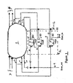
- FIG. 1 shows a scan test circuit
- FIG. 2 shows a circuit for power reduction in module-based scan testing.
- Scan test is a design technique that increases the testability of a primary circuit by replacing all or some of its storage elements by scan storage elements.
- the scan storage elements apply input stimulus to the primary circuit and then measure the response of the primary circuit to that input stimulus. Faults contained in the primary circuit are detected through this process.
- FIG. 1 depicts a circuit for conducting a scan test of the circuitry of an integrated circuit device.
- the circuitry related to the primary device is commonly called 'core logic'. Because of the large size of integrated circuits, it is often partitioned into sub-circuits.
- the sub-circuit core logic, 1 is coupled to a scan chain, 2, (described in detail next).
- Sub-circuit core logic 1 has primary inputs, 3, and primary outputs, 4. The primary inputs 3 and primary outputs 4 are used by the sub-circuit core logic 1 during the normal operation of the primary device.
- a scan chain 2 performs the scan testing of sub-circuit core logic 1.
- the example scan chain 2 shown in FIG. 1 is comprised of memory elements, 5, 6, 7, which are multiplexed scan flip-flops. These flip-flops are connected as a shift register to form the scan chain 2. During normal operation the flip-flops capture values from (on lines 13, 14, 15) and provide inputs to (on lines 10, 11, 12) the combinational logic of the sub-circuit core logic 1.
- test pattern is sent to the scan chain 2 through the Scan-in input, 8, connected to the SD input of the first flip-flop 5.
- the Q output of the last flip-flop 7 in the shift register is connected to Scan_out 9. (The Q output of the last flip-flop 7 is also connected through line 10 to the sub-circuit core logic 1, for use during normal circuit operation.)
- the tester When scan testing is performed on sub-circuit core logic 1 the tester (not shown) sends a test pattern on line 8 to the scan chain 2.
- the SE input, 16, is set to a logic level 1 by the tester during this procedure in order to load the test pattern onto the flip-flops through their SD inputs.
- the tester pulses the clock as many times as the length of the scan chain to load the full test pattern into the scan chain 2.
- the tester sends signals to the primary inputs 3 of the sub-circuit core logic 1.
- the tester then applies a capture clock and sets SE, line 16, to a logic level 0 in order to capture the responsive output values of the sub-circuit core logic into the flip-flops of scan chain 2.
- the tester drives SE to a logic level 1 and shifts into the scan chain 2 the next test pattern while simultaneously receiving the contents of the scan chain via Scan_out 9 for analysis and fault detection.
- circuitry 21 is the sub-circuit core logic of core 20; while circuitry 31 is the sub-circuit core logic of core 30.
- scan chain 22 is similar to scan chain 2 of FIG. 1 and belongs to core 20; while scan chain 32 is also similar to scan chain 2 of FIG. 1 and it belongs to core 30.
- the configuration shown in FIG. 2 is used in situations where scan pins are shared between scan chains belonging to different cores/modules. This configuration facilitates the use of a subset of the scan chains at any given point in time, resulting in reduced power consumption during the test process.
- This test procedure is often used in core-based designs where scan testing of one core can be performed followed by the scan testing of another core in the same design.
- Scan_in 40 is the scan input signal for both scan chains 22 and 32.
- Scan_out 41 is the scan output signal for both scan chains and is driven by either scan chain 22 or 32 based on the value of the "select" signal of multiplexer 42.
- the example application also shows the use of an optional asynchronous RESET or PRESET for scan chains 22 and 32.
- the RESET feature would be used in situations where the logic level of the test pattern sent to unused scan chains is a '0'.
- the PRESET feature would be used in situations where the logic level of the test pattern sent to unused scan chains is a '1'. If a RESET or PRESET is not used, then the first test pattern flushes out the pre-existing data in the scan chain and initializes the scan chain for subsequent receipt of the constant data input pattern.
- the unused scan chains are kept in scan shift mode by holding the SE pin, 47, at a logic 1 level during the time that the constant data is provided to the unused scan chains.
- select is a logic level 0
- RESET is triggered on scan chain 32 to initialize its' flip-flops to the '0' state. This prepares scan chain 32 to operate at a reduced power level while receiving constant '0' data.
- the constant '0' data is received by scan chain 32 on SD input 33 because select on multiplexer 45 is '0'.
- select on multiplexer 46 being '0' causes SE input 34 to hold at a logic level '1'.
- multiplexer 43 transfers the test pattern data from the tester, on Scan_in 40, to the SD input, 23, of scan chain 22.
- Multiplexer 44 with select at '0', pulls the SE input, 24, to a '0' value. This facilitates the capture by the scan chain flip-flops of the response of the sub-circuit logic 21 to the test pattern stimulus.
- the responsive data is then shifted out of the scan chain 22 on line 25, and sent to the tester for analysis on Scan_out 41 since select is at '0' on multiplexer 42.
- This invention is also applicable to situations where the test procedure described in FIG. 2 is expanded to numerous chains per core/module.
- the multiplexers such as 43 and 45
- Scan_in 40 would have inputs corresponding to each scan chain (such as 22 and 32) and select between the scan chains with a multi-bit select (for example, 1...sel [log 2 n ] ).
- the multiplexers associated with SE such as 44 and 46
- SE would need to be able to select between multiple scan chains. This configuration would allow for one or more scan chains to test sub-circuit core logic while the remaining, unused, scan chains received constant data.
- this invention could be realized with many different circuit or logic configurations.
- the scan circuitry could be created using transistor gates, AND/OR structures, pass transistor logic, switches, PLA's, ASIC's, DSP's, etc.
Landscapes
- Engineering & Computer Science (AREA)
- General Engineering & Computer Science (AREA)
- Physics & Mathematics (AREA)
- General Physics & Mathematics (AREA)
- Power Engineering (AREA)
- Tests Of Electronic Circuits (AREA)
- Semiconductor Integrated Circuits (AREA)
- Test And Diagnosis Of Digital Computers (AREA)
- Power Sources (AREA)
Abstract
Description
The Q output of the last flip-flop 7 in the shift register is connected to Scan_out 9. (The Q output of the last flip-flop 7 is also connected through line 10 to the
Claims (14)
- A method of scan testing an integrated circuit comprising:testing said integrated circuit using at least two scan chains; whereby transitions in a subset of said scan chains are minimized through the use of constant input data.
- A method of scan testing an integrated circuit having multiple cores comprising wherein the method of claim 1 is applied to each of said cores.
- A method of scan testing as claimed in any preceding claim wherein the subject includes a scan chain which is not being used for testing.
- A method as claimed in any preceding claim comprising:performing a reset of all of said scan chains that will not be used for the next test pattern;providing a constant data level throughout said test pattern to said scan chains that will not be used for the next test pattern.
- The method of any preceding claim wherein said constant data level is a logic level 0.
- A method as claimed in any of claims 1 to 4 comprising:performing a preset of all of said scan chains that will not be used for the next test pattern;providing a constant data level throughout said test pattern to said scan chains that will not be used for the next test pattern.
- The method of claim 6 wherein said constant data level is a logic level 1.
- An integrated circuit comprising:means for reducing transitions in scan test chains not used in test.
- An integrated circuit as claimed in claim 8 comprising:means for providing constant data to inputs of scan test chains not used in testing.
- An integrated circuit as claimed in claim 8 or claim 9 comprising:scanable flip-flops forming at least two scan chains; multiplexers and tie logic coupled to said scan chains; whereby said multiplexers and tie logic provides constant data levels to scan inputs of said scan chains not used in testing.
- An integrated circuit as claimed in claim 10 wherein comprising:said scan chains have asynchronous reset capability.
- The circuit of any of claims 8 to 11 wherein said constant data levels are a logic level 0.
- An integrated circuit as claimed in claim 10 wherein comprising:said scan chains have asynchronous preset capability.
- The circuit of claim 13 wherein said constant data levels are a logic level 1.
Applications Claiming Priority (2)
| Application Number | Priority Date | Filing Date | Title |
|---|---|---|---|
| US28663201P | 2001-04-26 | 2001-04-26 | |
| US286632P | 2001-04-26 |
Publications (2)
| Publication Number | Publication Date |
|---|---|
| EP1253432A2 true EP1253432A2 (en) | 2002-10-30 |
| EP1253432A3 EP1253432A3 (en) | 2003-03-26 |
Family
ID=23099466
Family Applications (1)
| Application Number | Title | Priority Date | Filing Date |
|---|---|---|---|
| EP02100414A Withdrawn EP1253432A3 (en) | 2001-04-26 | 2002-04-25 | Power reduction in module-based scan testing |
Country Status (3)
| Country | Link |
|---|---|
| US (2) | US20020170010A1 (en) |
| EP (1) | EP1253432A3 (en) |
| JP (1) | JP2003028934A (en) |
Families Citing this family (7)
| Publication number | Priority date | Publication date | Assignee | Title |
|---|---|---|---|---|
| JP3981281B2 (en) * | 2002-02-14 | 2007-09-26 | 松下電器産業株式会社 | Semiconductor integrated circuit design method and test method |
| US7188286B2 (en) * | 2003-01-24 | 2007-03-06 | On-Chip Technologies, Inc. | Accelerated scan circuitry and method for reducing scan test data volume and execution time |
| US7406639B2 (en) * | 2004-12-13 | 2008-07-29 | Lsi Corporation | Scan chain partition for reducing power in shift mode |
| CN100353290C (en) * | 2004-12-30 | 2007-12-05 | 普诚科技股份有限公司 | Power Saving Methods Using Scan Chains and Boundary Scan |
| US7669098B2 (en) * | 2006-12-07 | 2010-02-23 | Synopsys, Inc. | Method and apparatus for limiting power dissipation in test |
| US7757137B2 (en) * | 2007-03-27 | 2010-07-13 | International Business Machines Corporation | Method and apparatus for on-the-fly minimum power state transition |
| US12032015B1 (en) * | 2022-11-15 | 2024-07-09 | Amazon Technologies, Inc. | Flexible input/output (I/O) allocation for integrated circuit scan testing |
Family Cites Families (15)
| Publication number | Priority date | Publication date | Assignee | Title |
|---|---|---|---|---|
| US6556044B2 (en) * | 2001-09-18 | 2003-04-29 | Altera Corporation | Programmable logic device including multipliers and configurations thereof to reduce resource utilization |
| JP2626920B2 (en) * | 1990-01-23 | 1997-07-02 | 三菱電機株式会社 | Scan test circuit and semiconductor integrated circuit device using the same |
| US5450415A (en) * | 1992-11-25 | 1995-09-12 | Matsushita Electric Industrial Co., Ltd. | Boundary scan cell circuit and boundary scan test circuit |
| US5617531A (en) * | 1993-11-02 | 1997-04-01 | Motorola, Inc. | Data Processor having a built-in internal self test controller for testing a plurality of memories internal to the data processor |
| US5592493A (en) * | 1994-09-13 | 1997-01-07 | Motorola Inc. | Serial scan chain architecture for a data processing system and method of operation |
| US5838694A (en) * | 1997-04-28 | 1998-11-17 | Credence Systems Corporation | Dual source data distribution system for integrated circuit tester |
| US6278956B1 (en) * | 1998-04-30 | 2001-08-21 | International Business Machines Corporation | Method of locating a failed latch in a defective shift register |
| US6314539B1 (en) * | 1998-10-21 | 2001-11-06 | Xilinx, Inc. | Boundary-scan register cell with bypass circuit |
| US6191603B1 (en) * | 1999-01-08 | 2001-02-20 | Agilent Technologies Inc. | Modular embedded test system for use in integrated circuits |
| JP4294159B2 (en) * | 1999-05-06 | 2009-07-08 | 株式会社ルネサステクノロジ | Semiconductor integrated circuit device |
| US6769080B2 (en) * | 2000-03-09 | 2004-07-27 | Texas Instruments Incorporated | Scan circuit low power adapter with counter |
| US6766487B2 (en) * | 2000-03-09 | 2004-07-20 | Texas Instruments Incorporated | Divided scan path with decode logic receiving select control signals |
| US6760876B1 (en) * | 2000-04-04 | 2004-07-06 | Silicon Graphics, Inc. | Scan interface chip (SIC) system and method for scan testing electronic systems |
| US6754863B1 (en) * | 2000-04-04 | 2004-06-22 | Silicon Graphics, Inc. | Scan interface chip (SIC) system and method for scan testing electronic systems |
| US6445640B1 (en) * | 2001-03-23 | 2002-09-03 | Sun Microsystems, Inc. | Method and apparatus for invalidating memory array write operations |
-
2002
- 2002-04-24 US US10/131,161 patent/US20020170010A1/en not_active Abandoned
- 2002-04-25 EP EP02100414A patent/EP1253432A3/en not_active Withdrawn
- 2002-04-26 JP JP2002126601A patent/JP2003028934A/en active Pending
-
2005
- 2005-12-16 US US11/305,581 patent/US20060107144A1/en not_active Abandoned
Also Published As
| Publication number | Publication date |
|---|---|
| US20020170010A1 (en) | 2002-11-14 |
| EP1253432A3 (en) | 2003-03-26 |
| JP2003028934A (en) | 2003-01-29 |
| US20060107144A1 (en) | 2006-05-18 |
Similar Documents
| Publication | Publication Date | Title |
|---|---|---|
| US6861866B2 (en) | System on chip (SOC) and method of testing and/or debugging the system on chip | |
| EP2428808B1 (en) | Integrated circuit with scan chain and chip testing method | |
| US8479068B2 (en) | Decoded register outputs enabling test clock to selected asynchronous domains | |
| EP0548585A2 (en) | Clocking mechanism for delay, short path and stuck-at testing | |
| US6815977B2 (en) | Scan cell systems and methods | |
| US9689924B2 (en) | Circuit for testing integrated circuits | |
| US7269770B1 (en) | AC coupled line testing using boundary scan test methodology | |
| US20130275824A1 (en) | Scan-based capture and shift of interface functional signal values in conjunction with built-in self-test | |
| WO2007140366A2 (en) | Testing components of i/o paths of an integrated circuit | |
| US7188285B2 (en) | Scan test circuit with reset control circuit | |
| US8700962B2 (en) | Scan test circuitry configured to prevent capture of potentially non-deterministic values | |
| US5898702A (en) | Mutual exclusivity circuit for use in test pattern application scan architecture circuits | |
| US20060107144A1 (en) | Power reduction in module-based scan testing | |
| JPH0440113A (en) | Flip-flop circuit | |
| US6081913A (en) | Method for ensuring mutual exclusivity of selected signals during application of test patterns | |
| WO1996015496A1 (en) | Self-resetting bypass control for scan test | |
| EP1776596B1 (en) | Testing of a circuit that has an asynchronous timing circuit | |
| US7644329B2 (en) | Integrated circuit testing method and related circuit thereof | |
| US7089471B2 (en) | Scan testing mode control of gated clock signals for flip-flops | |
| JP2003121497A (en) | Scan path circuit for logic circuit test and integrated circuit device having the same | |
| US5793777A (en) | System and method for testing internal nodes of an integrated circuit at any predetermined machine cycle | |
| KR100694315B1 (en) | Cable Delay Failure Test Controller for System-on-Chip with Multiple System Clocks and Heterogeneous Cores | |
| US7747916B2 (en) | JTAG interface | |
| CN223666334U (en) | Signal generation circuit, boundary scan unit, circuits and electronic equipment | |
| JP3328160B2 (en) | Test equipment for logic integrated circuits |
Legal Events
| Date | Code | Title | Description |
|---|---|---|---|
| PUAI | Public reference made under article 153(3) epc to a published international application that has entered the european phase |
Free format text: ORIGINAL CODE: 0009012 |
|
| AK | Designated contracting states |
Kind code of ref document: A2 Designated state(s): AT BE CH CY DE DK ES FI FR GB GR IE IT LI LU MC NL PT SE TR |
|
| AX | Request for extension of the european patent |
Free format text: AL;LT;LV;MK;RO;SI |
|
| PUAL | Search report despatched |
Free format text: ORIGINAL CODE: 0009013 |
|
| AK | Designated contracting states |
Kind code of ref document: A3 Designated state(s): AT BE CH CY DE DK ES FI FR GB GR IE IT LI LU MC NL PT SE TR Designated state(s): AT BE CH CY DE DK ES FI FR GB GR IE IT LI LU MC NL PT SE TR |
|
| AX | Request for extension of the european patent |
Extension state: AL LT LV MK RO SI |
|
| 17P | Request for examination filed |
Effective date: 20030926 |
|
| AKX | Designation fees paid |
Designated state(s): DE FR GB |
|
| 17Q | First examination report despatched |
Effective date: 20061108 |
|
| STAA | Information on the status of an ep patent application or granted ep patent |
Free format text: STATUS: THE APPLICATION IS DEEMED TO BE WITHDRAWN |
|
| 18D | Application deemed to be withdrawn |
Effective date: 20070519 |