EP1251720A2 - Organic semiconductor diode and organic electroluminescence element display device - Google Patents
Organic semiconductor diode and organic electroluminescence element display device Download PDFInfo
- Publication number
- EP1251720A2 EP1251720A2 EP02252144A EP02252144A EP1251720A2 EP 1251720 A2 EP1251720 A2 EP 1251720A2 EP 02252144 A EP02252144 A EP 02252144A EP 02252144 A EP02252144 A EP 02252144A EP 1251720 A2 EP1251720 A2 EP 1251720A2
- Authority
- EP
- European Patent Office
- Prior art keywords
- transport layer
- organic
- hole transport
- electron transport
- organic semiconductor
- Prior art date
- Legal status (The legal status is an assumption and is not a legal conclusion. Google has not performed a legal analysis and makes no representation as to the accuracy of the status listed.)
- Withdrawn
Links
Images


Classifications
-
- H—ELECTRICITY
- H10—SEMICONDUCTOR DEVICES; ELECTRIC SOLID-STATE DEVICES NOT OTHERWISE PROVIDED FOR
- H10K—ORGANIC ELECTRIC SOLID-STATE DEVICES
- H10K10/00—Organic devices specially adapted for rectifying, amplifying, oscillating or switching; Organic capacitors or resistors having potential barriers
- H10K10/20—Organic diodes
- H10K10/26—Diodes comprising organic-organic junctions
-
- H—ELECTRICITY
- H10—SEMICONDUCTOR DEVICES; ELECTRIC SOLID-STATE DEVICES NOT OTHERWISE PROVIDED FOR
- H10K—ORGANIC ELECTRIC SOLID-STATE DEVICES
- H10K59/00—Integrated devices, or assemblies of multiple devices, comprising at least one organic light-emitting element covered by group H10K50/00
- H10K59/10—OLED displays
- H10K59/17—Passive-matrix OLED displays
-
- H—ELECTRICITY
- H10—SEMICONDUCTOR DEVICES; ELECTRIC SOLID-STATE DEVICES NOT OTHERWISE PROVIDED FOR
- H10K—ORGANIC ELECTRIC SOLID-STATE DEVICES
- H10K85/00—Organic materials used in the body or electrodes of devices covered by this subclass
- H10K85/30—Coordination compounds
-
- H—ELECTRICITY
- H10—SEMICONDUCTOR DEVICES; ELECTRIC SOLID-STATE DEVICES NOT OTHERWISE PROVIDED FOR
- H10K—ORGANIC ELECTRIC SOLID-STATE DEVICES
- H10K85/00—Organic materials used in the body or electrodes of devices covered by this subclass
- H10K85/30—Coordination compounds
- H10K85/311—Phthalocyanine
-
- H—ELECTRICITY
- H10—SEMICONDUCTOR DEVICES; ELECTRIC SOLID-STATE DEVICES NOT OTHERWISE PROVIDED FOR
- H10K—ORGANIC ELECTRIC SOLID-STATE DEVICES
- H10K85/00—Organic materials used in the body or electrodes of devices covered by this subclass
- H10K85/30—Coordination compounds
- H10K85/321—Metal complexes comprising a group IIIA element, e.g. Tris (8-hydroxyquinoline) gallium [Gaq3]
- H10K85/324—Metal complexes comprising a group IIIA element, e.g. Tris (8-hydroxyquinoline) gallium [Gaq3] comprising aluminium, e.g. Alq3
-
- H—ELECTRICITY
- H10—SEMICONDUCTOR DEVICES; ELECTRIC SOLID-STATE DEVICES NOT OTHERWISE PROVIDED FOR
- H10K—ORGANIC ELECTRIC SOLID-STATE DEVICES
- H10K85/00—Organic materials used in the body or electrodes of devices covered by this subclass
- H10K85/60—Organic compounds having low molecular weight
-
- H—ELECTRICITY
- H10—SEMICONDUCTOR DEVICES; ELECTRIC SOLID-STATE DEVICES NOT OTHERWISE PROVIDED FOR
- H10K—ORGANIC ELECTRIC SOLID-STATE DEVICES
- H10K85/00—Organic materials used in the body or electrodes of devices covered by this subclass
- H10K85/60—Organic compounds having low molecular weight
- H10K85/615—Polycyclic condensed aromatic hydrocarbons, e.g. anthracene
-
- H—ELECTRICITY
- H10—SEMICONDUCTOR DEVICES; ELECTRIC SOLID-STATE DEVICES NOT OTHERWISE PROVIDED FOR
- H10K—ORGANIC ELECTRIC SOLID-STATE DEVICES
- H10K85/00—Organic materials used in the body or electrodes of devices covered by this subclass
- H10K85/60—Organic compounds having low molecular weight
- H10K85/615—Polycyclic condensed aromatic hydrocarbons, e.g. anthracene
- H10K85/621—Aromatic anhydride or imide compounds, e.g. perylene tetra-carboxylic dianhydride or perylene tetracarboxylic di-imide
-
- H—ELECTRICITY
- H10—SEMICONDUCTOR DEVICES; ELECTRIC SOLID-STATE DEVICES NOT OTHERWISE PROVIDED FOR
- H10K—ORGANIC ELECTRIC SOLID-STATE DEVICES
- H10K85/00—Organic materials used in the body or electrodes of devices covered by this subclass
- H10K85/60—Organic compounds having low molecular weight
- H10K85/631—Amine compounds having at least two aryl rest on at least one amine-nitrogen atom, e.g. triphenylamine
Definitions
- the present invention relates to an organic semiconductor, i.e. a two-terminal element diode which exhibits a nonlinear current-voltage characteristics by the movement of electrons and holes supplied to the junction of thin films made of organic compounds having electrical characteristics different from each other and to an organic electroluminescence element display device using the same.
- an organic semiconductor i.e. a two-terminal element diode which exhibits a nonlinear current-voltage characteristics by the movement of electrons and holes supplied to the junction of thin films made of organic compounds having electrical characteristics different from each other and to an organic electroluminescence element display device using the same.
- organic electroluminescence element (hereinafter also referred to as “organic EL element”) which makes use of electroluminescence (hereinafter also referred to as "EL") of an organic compound that emits light by injection of electric current and includes a light-emitting layer formed by a thin layer of such an organic compound.
- EL element display device formed by arranging a plurality of the above organic EL elements in a matrix form is receiving attention as a display device capable of achieving low power consumption, high display quality, and thickness reduction. As shown in FIG.
- each organic EL element 200 is comprised of a transparent substrate 1, such as a glass plate or the like, a transparent anode electrode 201 formed on the substrate, at least one organic material layer 202 which is comprised of an electron transport layer, a light-emitting layer, and a hole transport layer, and a metal cathode electrode 203, all of which are laminated in the mentioned order.
- a positive voltage is applied to the transparent anode electrode 201
- a negative voltage is applied to the metal cathode electrode 203, that is, when a direct current is caused to flow between the transparent electrode and the metal electrode, the light-emitting layer in the organic material layer 202 emits light.
- the organic EL element is considered as a capacitive light-emitting element.
- a direct current driving voltage for causing light emission is applied between the electrodes, an electric charge is accumulated in a capacity component. Then, when the driving voltage exceeds a light-emitting threshold voltage of the EL element, a current starts to flow in the organic material layer to cause the organic EL element to emit light at a luminous intensity approximately proportional to the current.
- the organic EL element display device is a light-emitting apparatus composed of a plurality of light-emitting pixels, that is, organic EL elements, in an image display layout in which the organic EL elements are disposed at respective points of intersection of horizontal lines and vertical lines, i.e. in a so-called matrix form.
- An example of the method of driving the organic EL element display device is a so-called simple matrix driving method.
- a display apparatus based on the simple matrix driving method has a plurality of anode lines and cathode lines arranged in the form of a matrix (grid), with organic EL elements connected at respective points of the intersection of the anode lines and the cathode lines.
- Either of the anode lines and the cathode lines are sequentially selected at predetermined time intervals for scanning, and the other lines are driven by a drive source in synchronism with the scanning, to cause organic EL elements arranged at desired points of intersection of the lines to emit light.
- each organic EL element is lighted only during an access time period, and hence to increase the size of a display screen of the apparatus, a large current and a high voltage are required.
- an active matrix driving method may be considered, besides the simple matrix driving method.
- the active matrix driving method uses a thin film transistor (TFT) arranged at each point of the intersection (of the anode lines and the cathode lines), and supplies a current to each pixel by switching operation to cause the associated organic EL element to emit light.
- TFT thin film transistor
- the TFT can be formed with using an element formed by p-Si or a-Si.
- MOS-FET Metal Oxide Semiconductor Field Effect Transistor
- the active matrix driving method requires a large number of switching circuit substrates, and inorganic materials have to be laminated on substrates of the circuits. Therefore, a high temperature process is employed for manufacturing the switching circuits.
- an object of the present invention is to provide an organic semiconductor diode which can be produced at a relatively low temperature
- another object of the present invention is to provide an organic EL element display device having the organic semiconductor diodes formed on a common substrate.
- a hole transport layer on the anode side has a smaller ionization potential than that of another hole transport layer.
- an electron transport layer on the cathode side has a larger electron affinity than that of another electron transport layer.
- An organic electroluminescence element display device having plural light-emitting portions arranged in a display layout according to a second aspect of the present invention comprises:
- At least one of said hole transport layer and said electron transport layer of said organic semiconductor diode is formed of the same organic compound as that of at least one of said light-emitting layer and said carrier transport layer.
- said organic semiconductor diode and said organic electroluminescence element are laminated one upon another.
- FIG. 2 shows an organic semiconductor diode according to an embodiment.
- the organic semiconductor diode 11 includes an insulating substrate 1 of glass or the like, an anode 2 formed on the insulating substrate 1, a hole transport layer 3 which is formed of an organic compound, an electron transport layer 4 which is formed of an organic compound, the hole transport layer 3 and the electron transport layer 4 having formed on the anode 2 such that they are in contact with each other, and a cathode 7 is laminated on the electron transport layer 4.
- the cathode 7 cooperates with the anode 2 opposed thereto to apply an electric field to the junction of the hole transport layer 3 and the electron transport layer 4. More specifically, the cathode 7 injects electrons into the electron transport layer 4 having an electron transporting property, whereas the anode 2 injects holes into the hole transport layer 3 having a hole transporting property.
- the organic semiconductor diode 11 is only required to be composed of a hole transport layer on the anode side and an electron transport layer on the cathode side, which are laminated one upon the other.
- the organic semiconductor diode 11 may have the components laminated on the substrate in the reverse order to that of the example illustrated in FIG. 2, that is , in the order of the cathode, the electron transport layer, the hole transport layer, and the anode.
- the hole transport layer is formed of an organic compound having a hole transport capability
- the electron transport layer is formed of an organic compound having an electron transport capability.
- the ionization potential of the hole transport layer on the anode side is larger than the electron affinity of the electron transport layer on the cathode side.
- the hole transport layer and the electron transport layer can be constructed such that they have multi-layer structures formed by thin films of organic compounds having a hole transport capability and an electron transport capability, respectively.
- the organic semiconductor diode exhibits nonlinear current-voltage characteristics when a voltage is applied between the hole transport layer and the electron transport layer in contact with each other.
- the cathode has a work function close to or smaller than the electron affinity of the electron transport layer, while the anode has a work function larger than that of the cathode.
- the electron affinity Ea is an energy measured from a vacuum level as the reference energy level of O eV to a lowest unoccupied molecular orbital (LUMO) level at a lower edge of a conduction band CB.
- the ionization potential Ip is an energy value measured from the vacuum level to a highest occupied molecular orbital (HOMO) level at an upper edge of a valence electron band VB.
- the work functions WfA and WfC at the respective anode and cathode are energies measured from the vacuum level (O eV) to respective Fermi levels, concerning a metal material and a metal oxide material.
- an anode material (ANODE) used for the organic semiconductor diode according to the present invention has a work function WfA as high as possible.
- ANODE anode material
- a conductive polymer such as poly (3-methylthiophene), polyphenylene sulfide, or polyaniline. These materials can be used separately or by laminating two or more kinds of them one upon the other, for instance, by laminating a polyaniline film on ITO film.
- a cathode material there is used a metal or a compound having a low work function WfC, for instance, an alkali metal, such as silver, lead, tin, aluminum, calcium, indium, chromium, or lithium, an alkaline-earth metal, such as magnesium, or an alloy of selected ones of these metals, or further an alkali metal compound, or an alkaline-earth metal compound, each of which has a work function lower than 4.5 eV.
- an alkali metal such as silver, lead, tin, aluminum, calcium, indium, chromium, or lithium
- an alkaline-earth metal such as magnesium, or an alloy of selected ones of these metals
- an alkali metal compound such as magnesium, or an alloy of selected ones of these metals
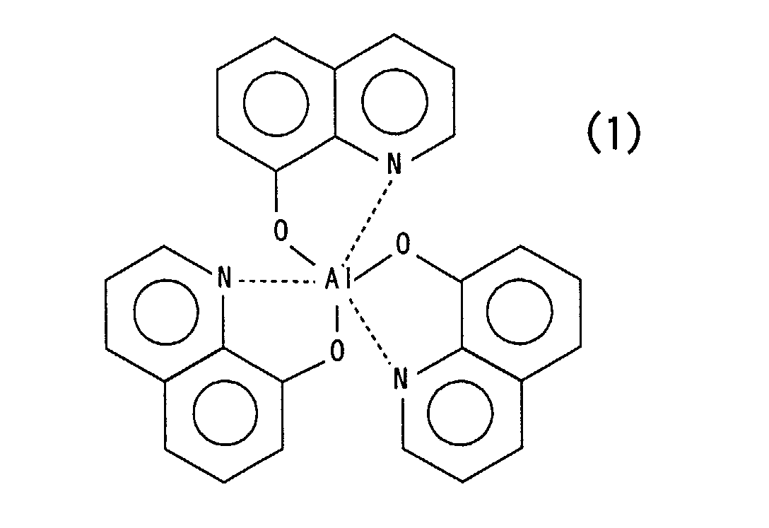
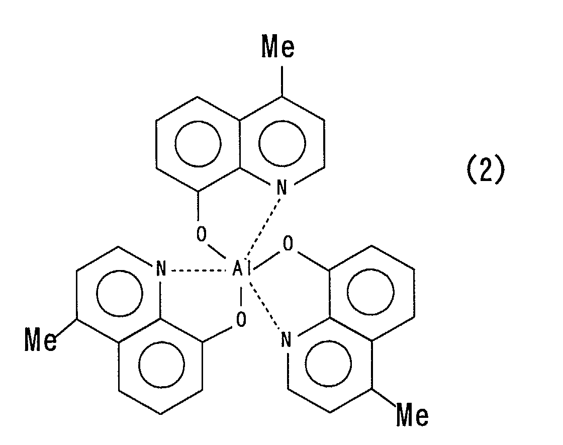
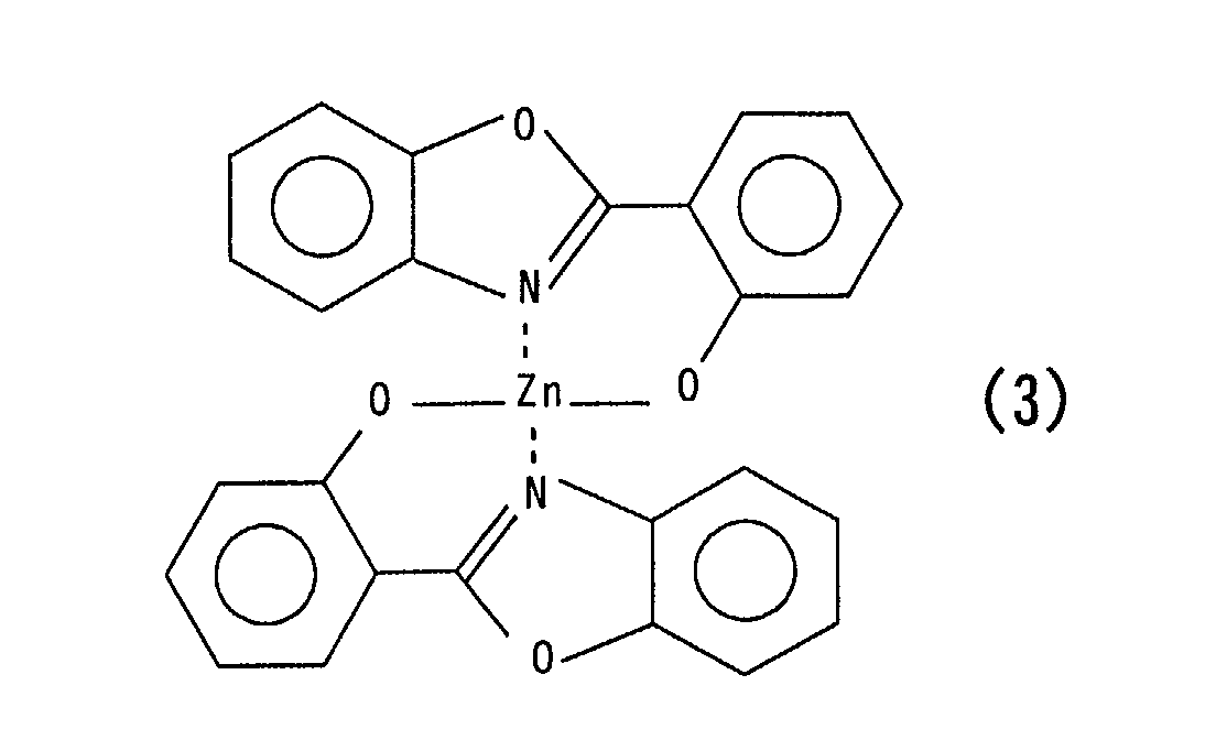
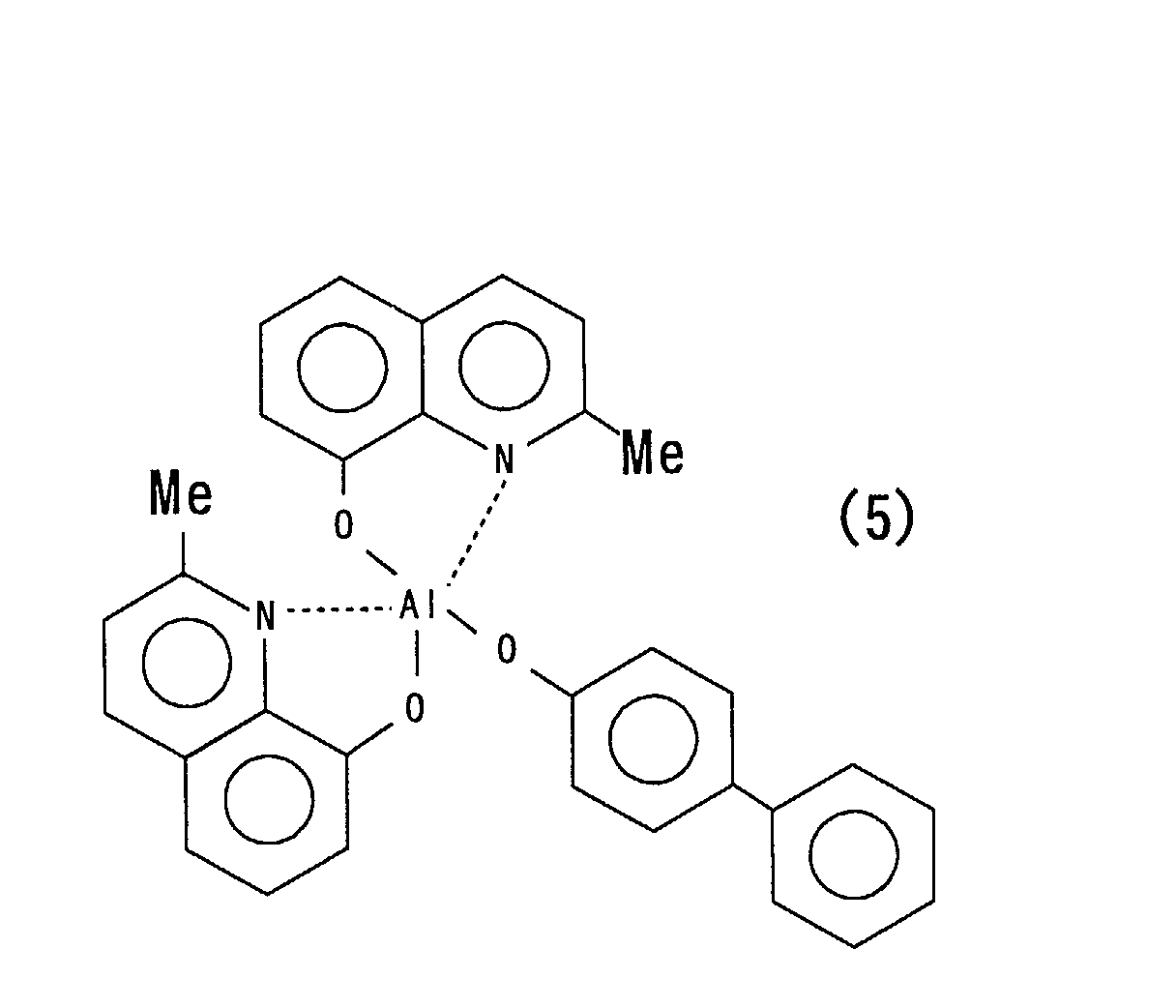
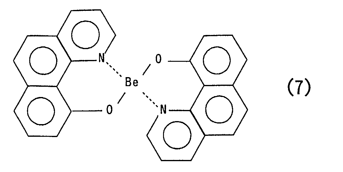
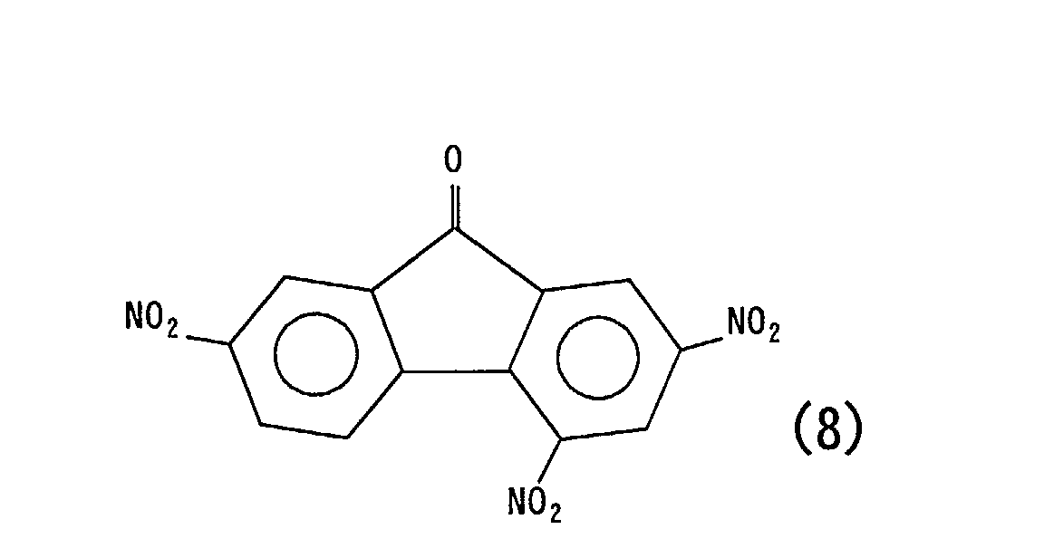
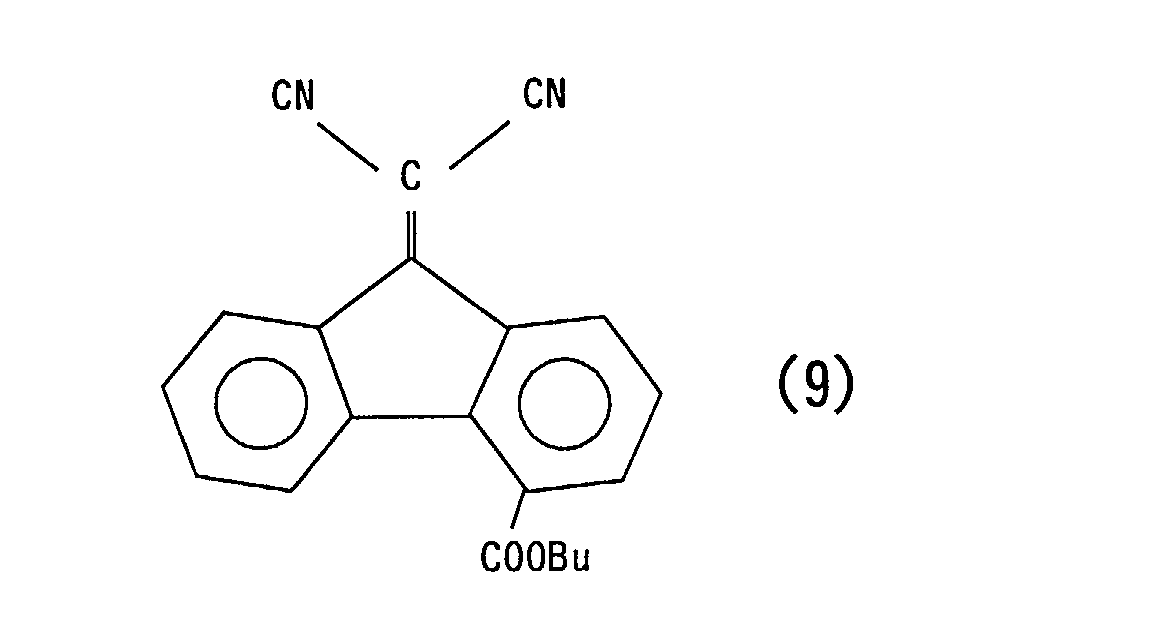
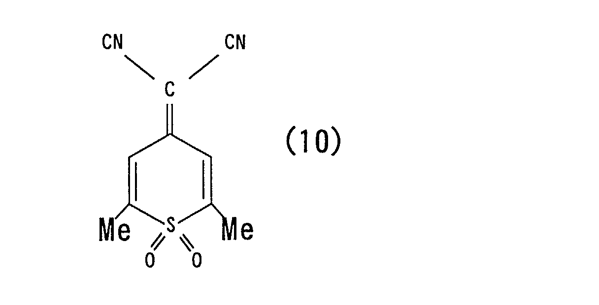
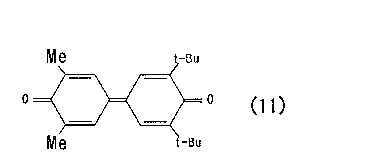
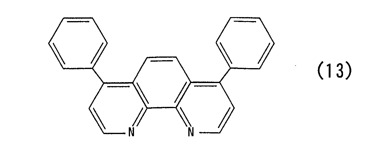
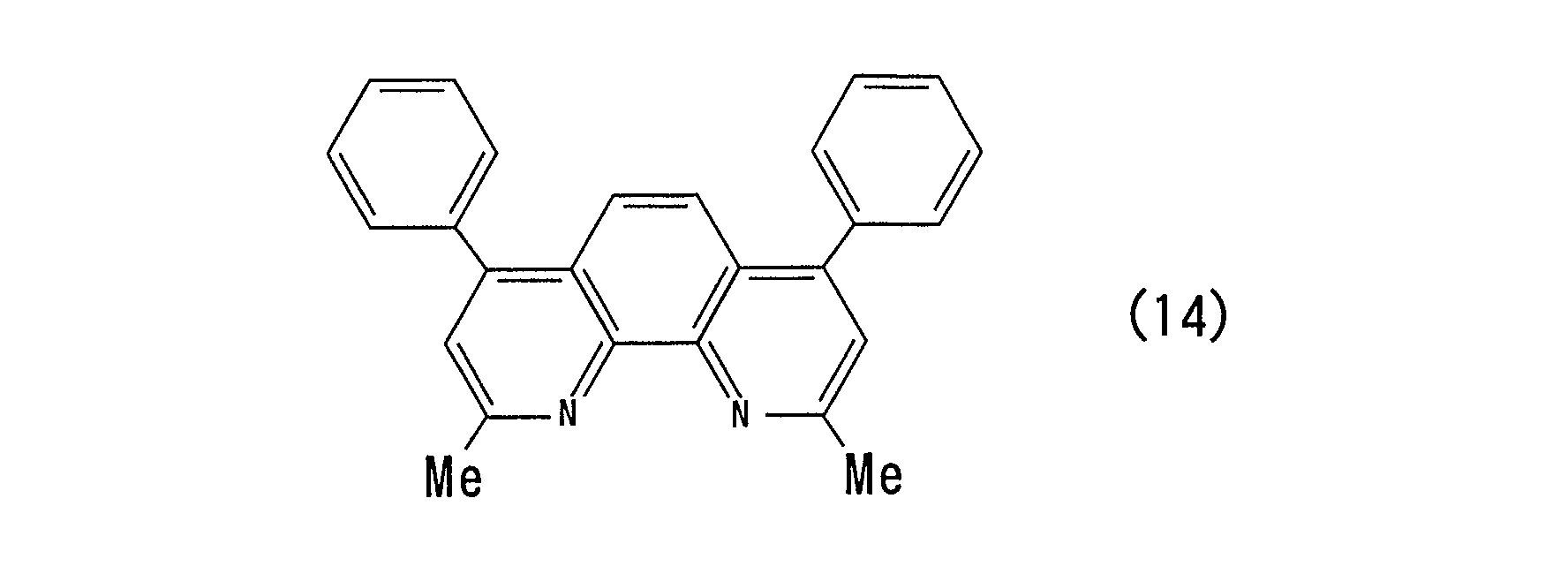
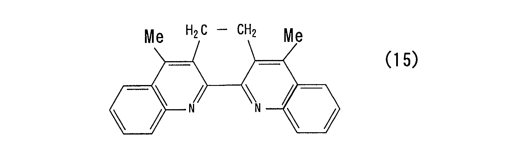
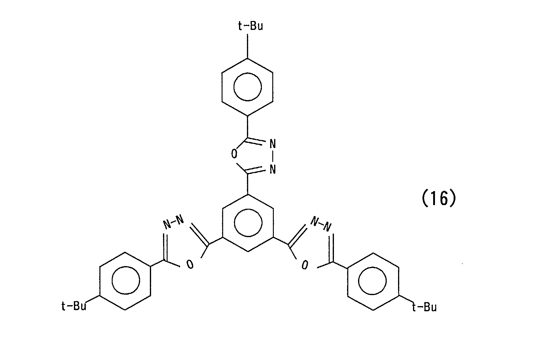
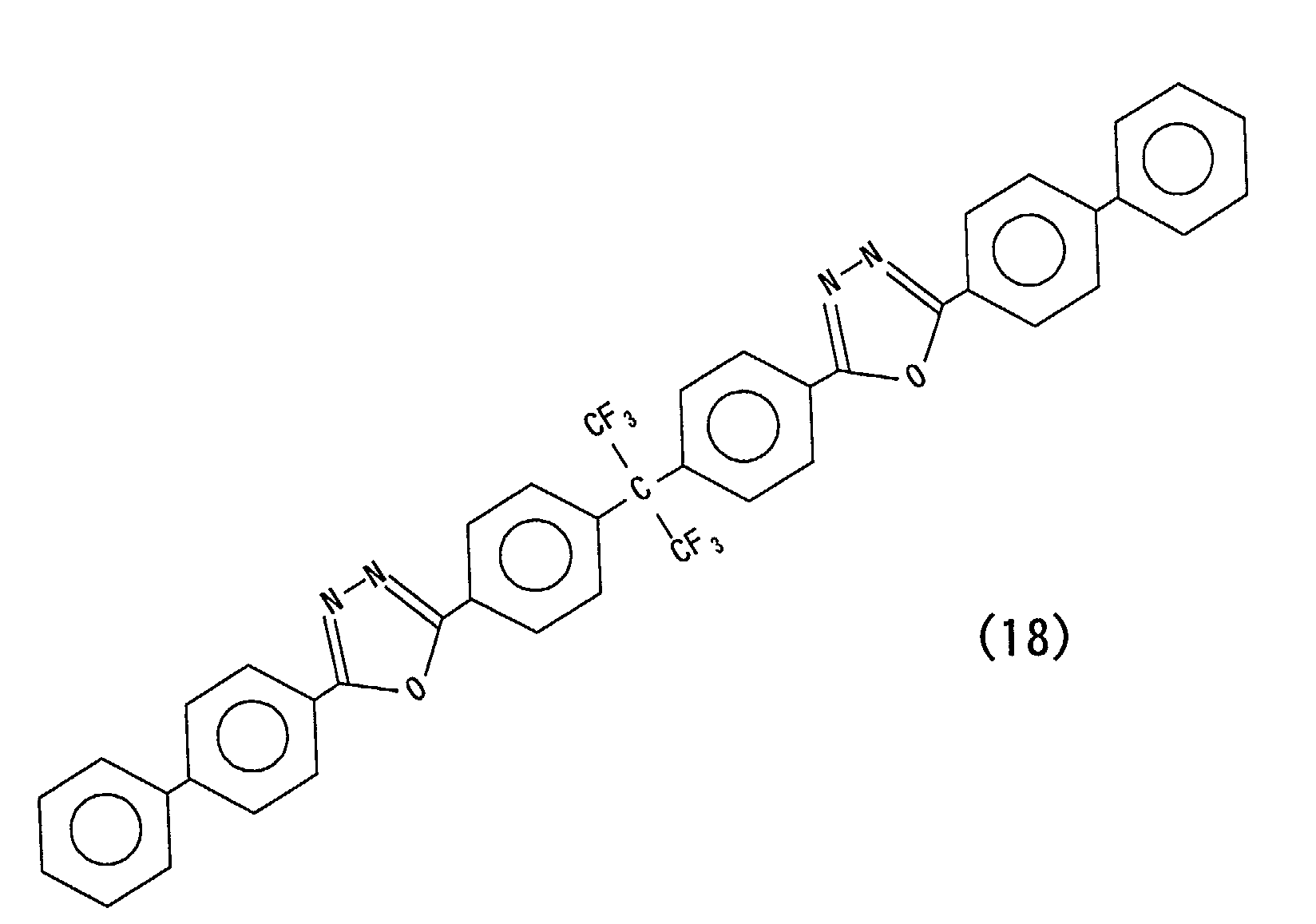
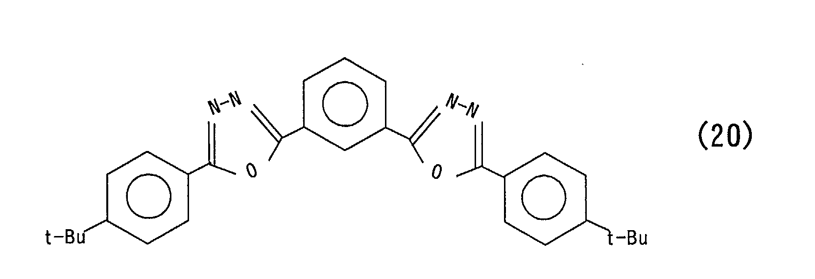
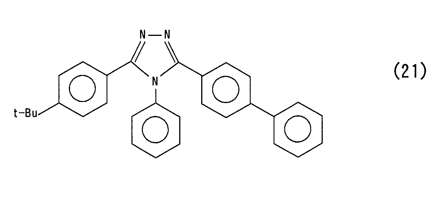
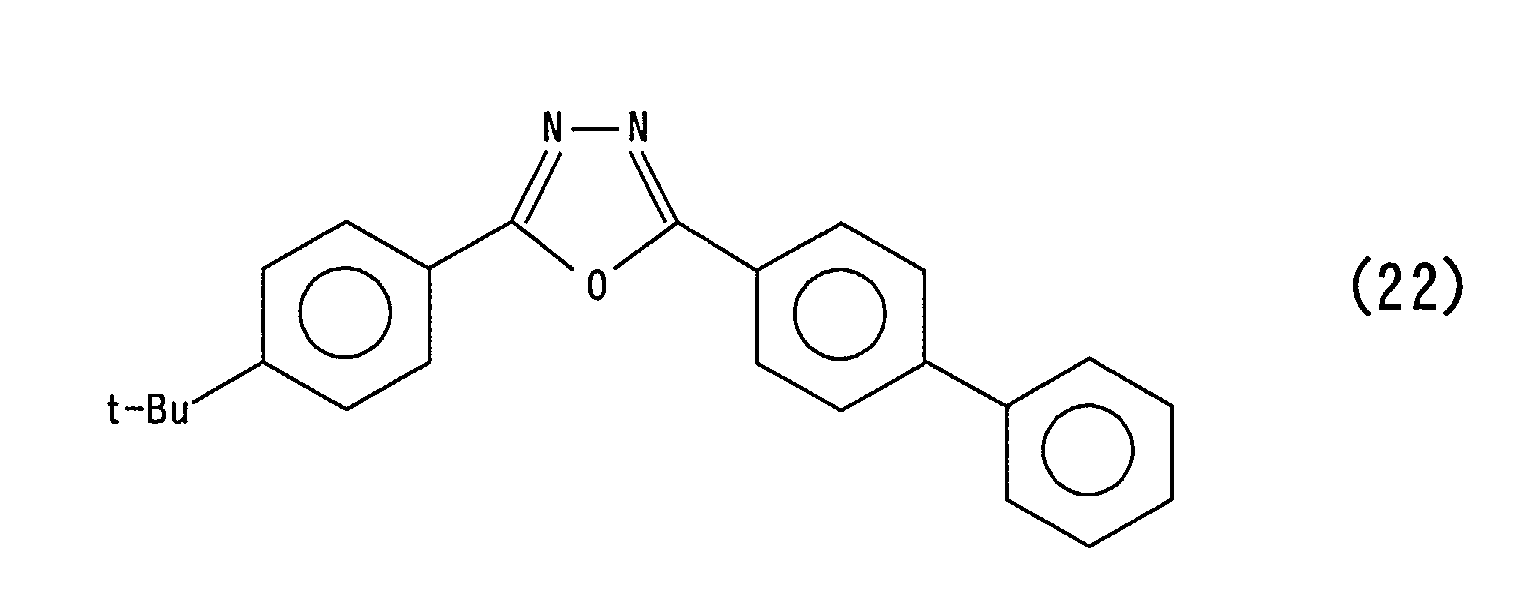
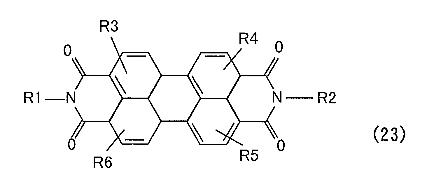
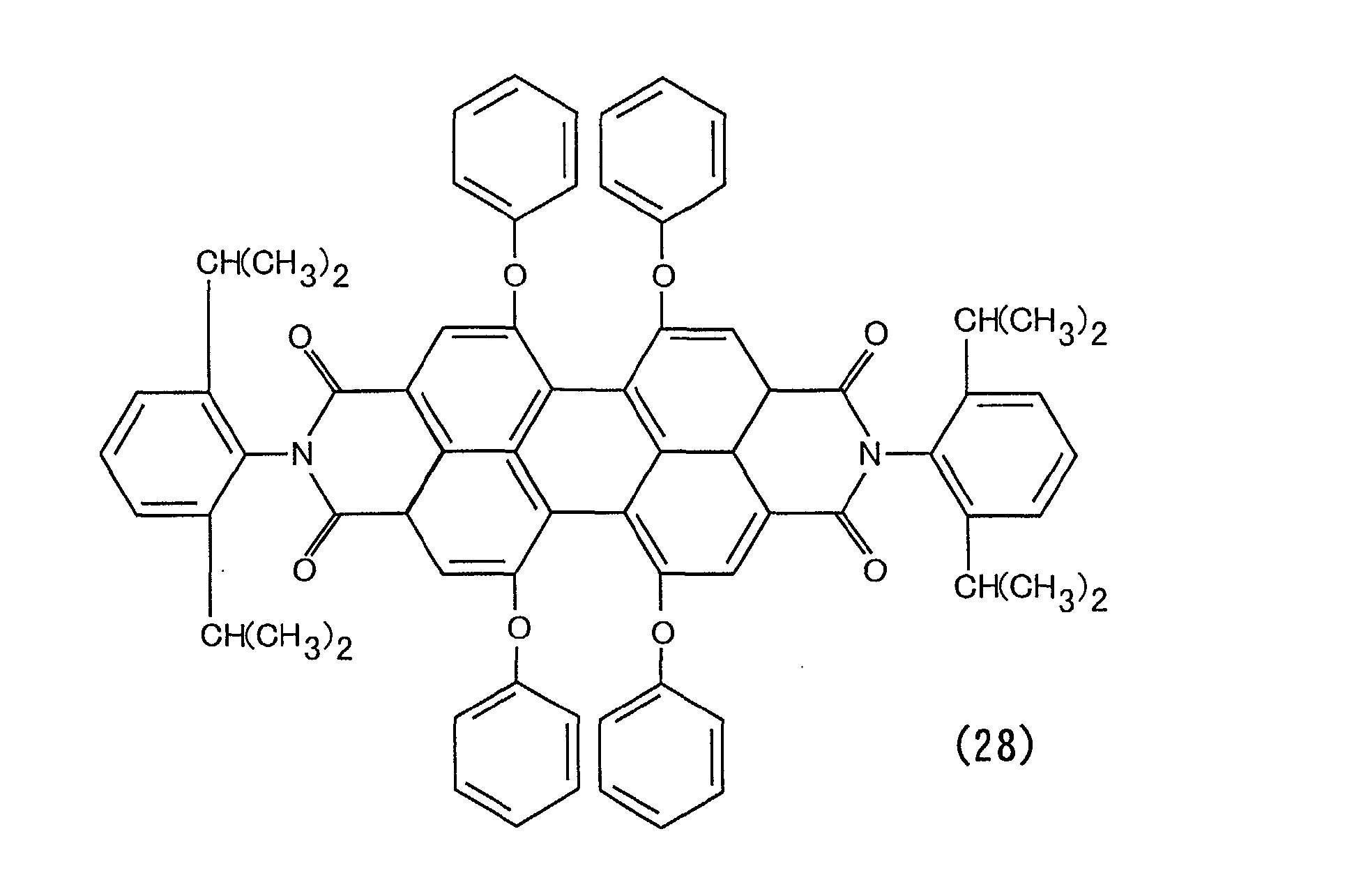
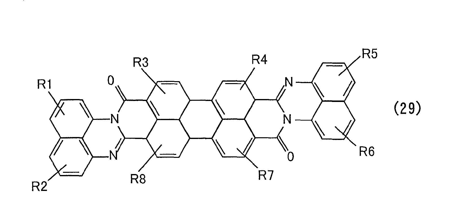
- the electron transport material of the electron transport layer which has an electron transport capability, is selected from organic compounds represented by the following formulas (1) to (35).
- the electron transport material N-TYPE ORGANICS
- Ea electron affinity
- an electron transport layer on the cathode side has a larger electron affinity than that of an electron transport layer on the anode side.
- R1 to R6 each independently represent hydrogen, an alkyl or alkoxy group having a carbon number of 1 to 12, an aryl or aryloxy group having a carbon number of 6 to 14, a heterocyclic compound group, a cyano group, a halogen group, a halogenated alkyl group, or a nitro group.
- R1 to R8 each independently represent hydrogen, an alkyl or alkoxy group having a carbon number of 1 to 12, an aryl or aryloxy group having a carbon number of 6 to 14, a heterocyclic compound group, a cyano group, a halogen group, a halogenated alkyl group, or a nitro group.
- R1 to R8 each independently represent hydrogen, an alkyl or alkoxy group having a carbon number of 1 to 12, an aryl or aryloxy group having a carbon number of 6 to 14, a heterocyclic compound group, a cyano group, a halogen group, a halogenated alkyl group, or a nitro group.
- R1 to R4 each independently represent hydrogen, an alkyl or alkoxy group having a carbon number of 1 to 12, an aryl or aryloxy group having a carbon number of 6 to 14, a heterocyclic compound group, a cyano group, a halogen group, a halogenated alkyl group, or a nitro group.
- condensed ring compounds such as a perylene derivative or the like, shown in the above formulas (23) to (35) are preferably used as materials having an electron transport capability, of the electron transport layer.
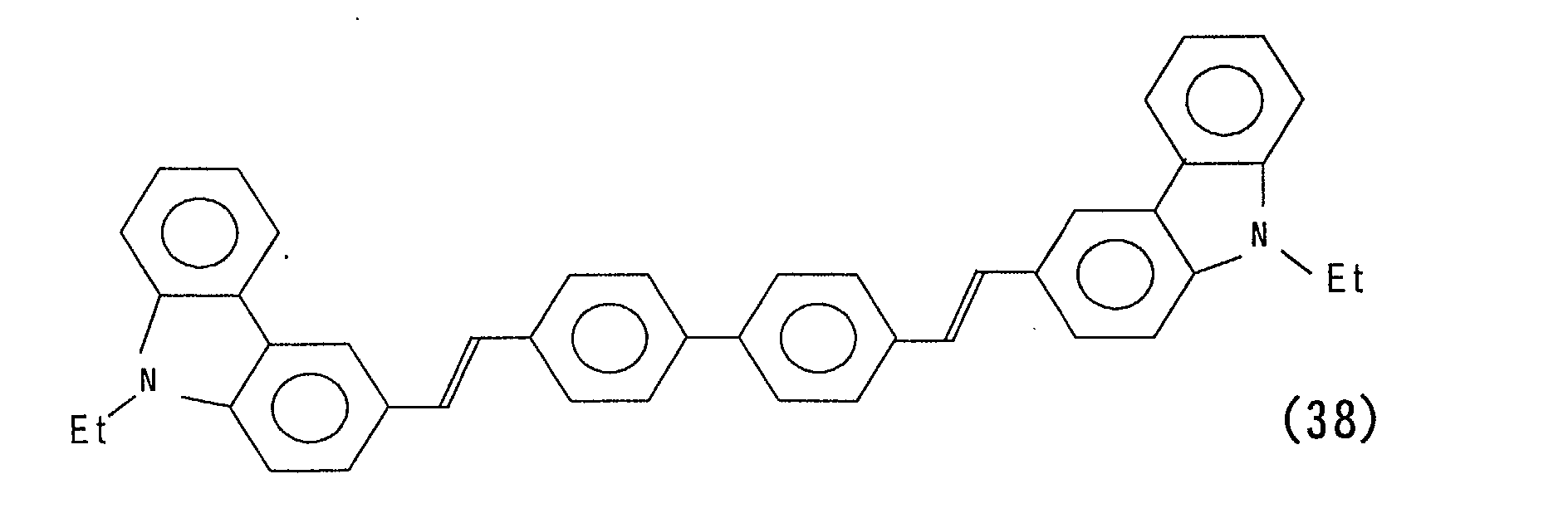
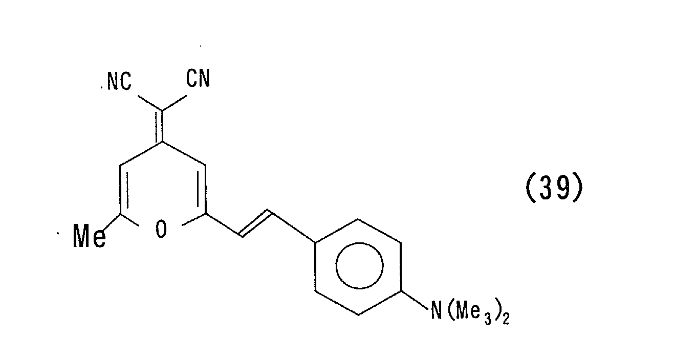
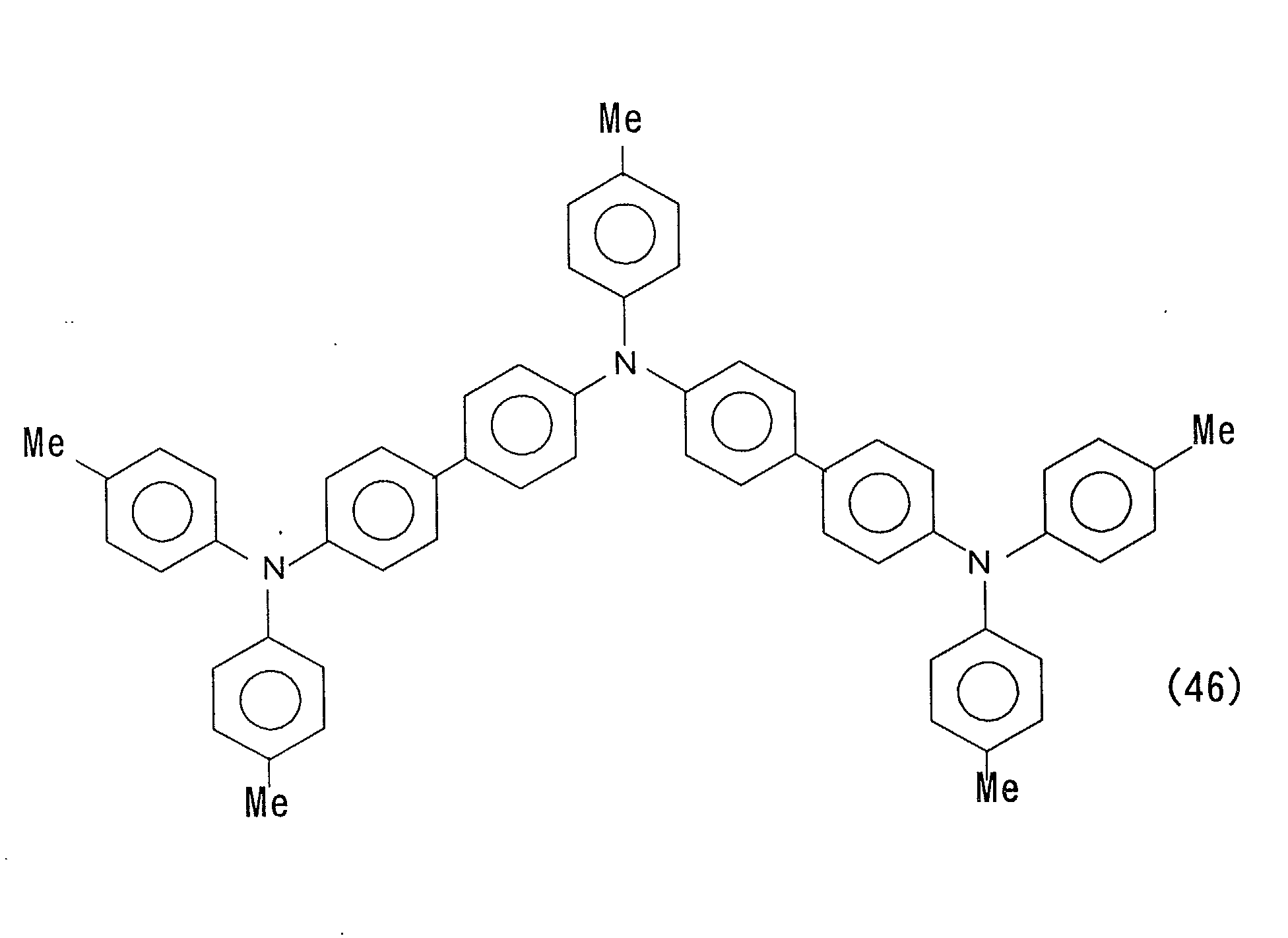
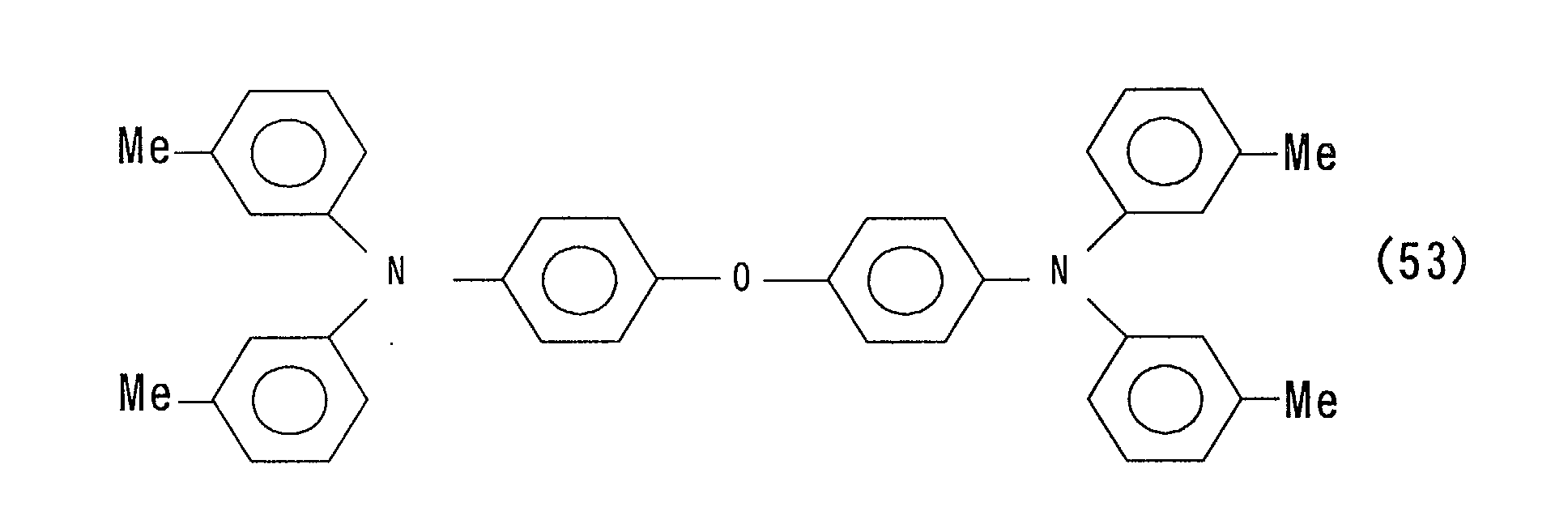
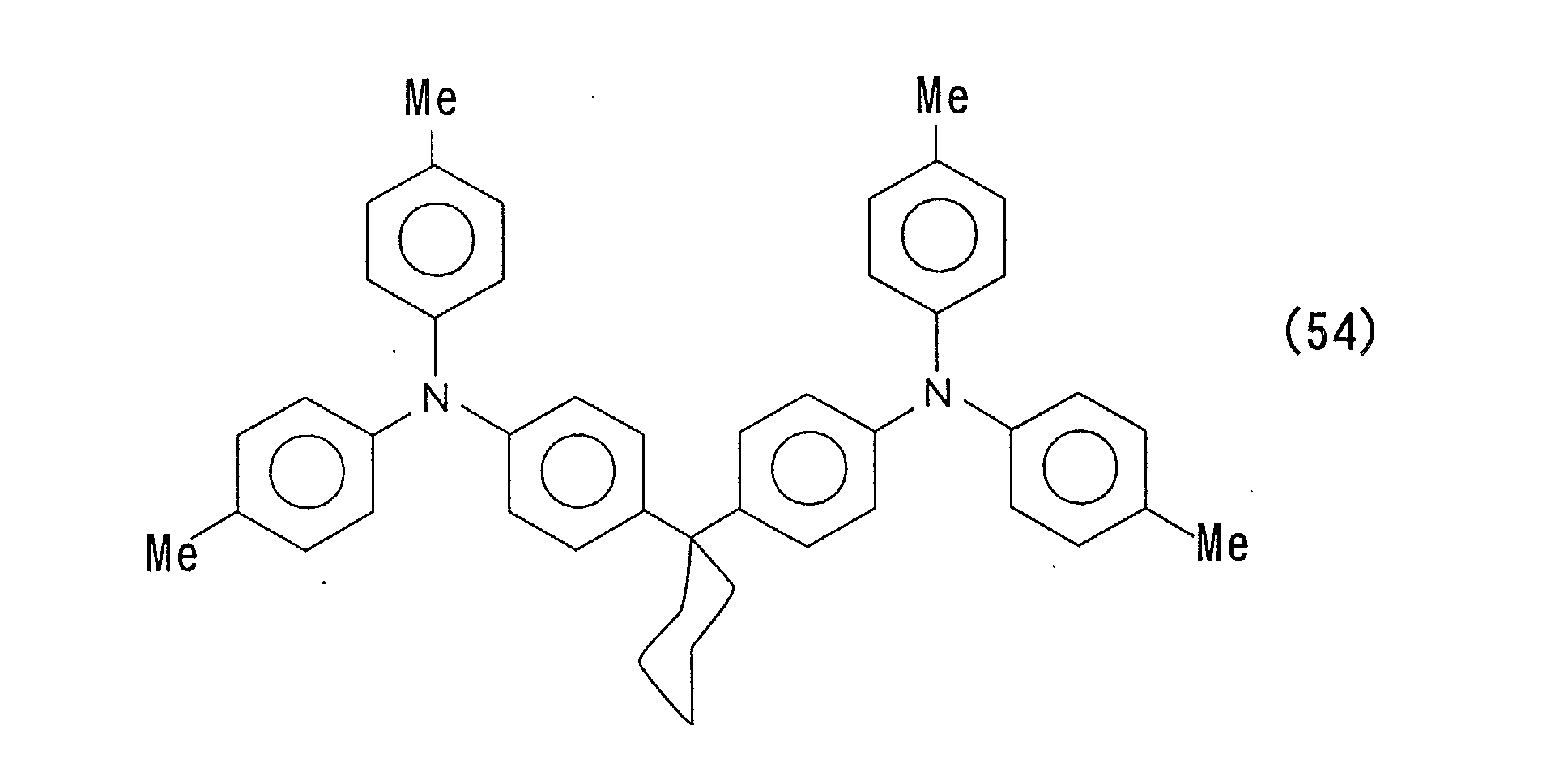
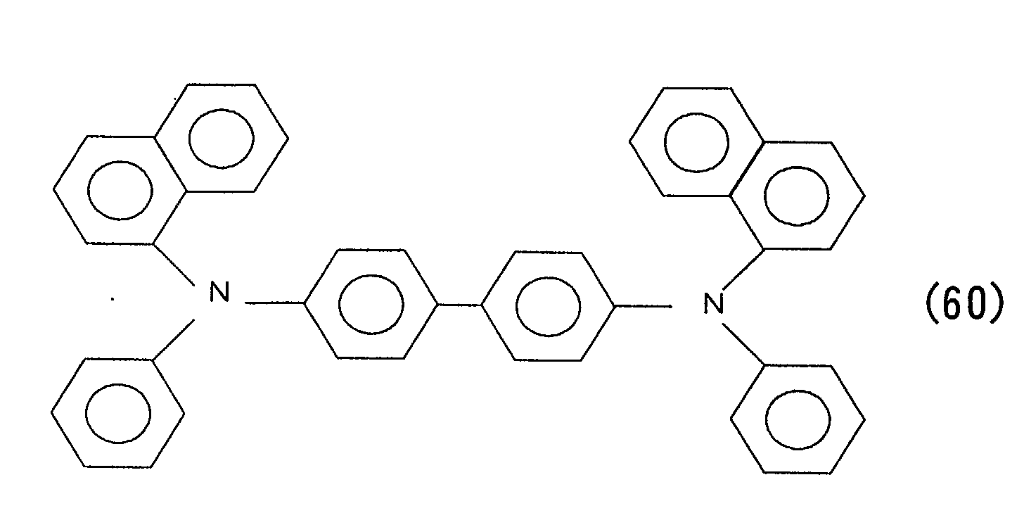
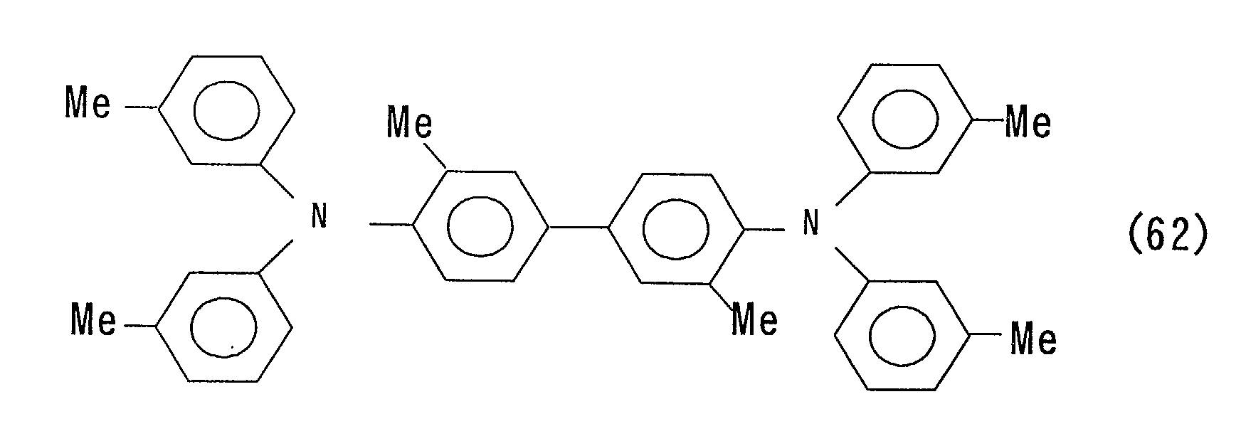
- the hole transport material of the hole transport layer which has a hole transport capability, is selected from organic compounds represented by the following formulas (36) to (64).
- the hole transport material P-TYPE ORGANICS
- Ip ionization potential
- Me designates a methyl group
- Et designates an ethyl group
- Bu designates a butyl group
- t-Bu designates a tertiary butyl group.
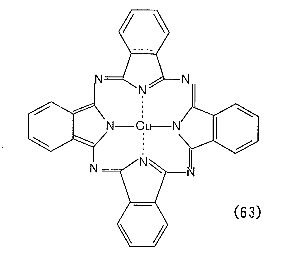
- the formula (63) represents copper phthalocyanine, that is called CuPc, having a hole transport capability, which is included in porphyrin derivatives.
- the porphyrin derivatives include the following materials which can be employed as hole transport layers:
- the layers may be doped with a fluorescence material or a phosphorescence material. Further, they may be doped with an inorganic or organic material for enhancing the carrier density of each layer.
- the hole transport layer or the electron transport layer may be formed by co-deposition as a mixture layer composed of a plurality of materials each of which is formed of an organic compound and has a transport capability. Further, the hole transport layer or the electron transport layer may be configured to have one or more mixture layers.
- the hole transport layer and the electron transport layer each composed of an organic compound are kinds of semiconductors which can be regarded as a p-type organic semiconductor material and an n-type organic semiconductor material (hereinafter also simply referred to as “the p-type material” and “the n-type material”), respectively.
- the inventors have found that it is possible to properly form an organic p-n junction by taking into account the electron affinity, ionization potential, electron energy band gap, Fermi level, and (carrier) mobility of each of the above organic transport materials as well as the thickness of each of thin films of the organic compounds, and obtain an organic semiconductor diode by using such an organic p-n junction.
- the electrical characteristics of laminate layers of thin films made of the above organic compounds different in electrical characteristics depend on the ionization potential, electron energy band gap, Fermi level and carrier mobility, and work functions at the anode and cathode, of each organic thin film layer, and determine the characteristics of the element itself.
- the organic p-n junction is formed by laminating two kinds of adjacent organic compound thin films different in energy band gap, one upon the other. During thermal equilibrium, the two kinds of organic compound materials have constant Fermi levels as a whole. The thermal equilibrium is achieved by diffusion of the carriers of free electrons and holes through the junction interface, and as a result, an inner electric field is generated within the junction.
- the inner electric field causes the vacuum level to move, and the end of the energy band to bend.
- An inner electric field generated between the conduction bands of the p-type material and the n-type organic material serves as a potential barrier for preventing electrons oozing out of the region of the n-type material from moving into the region of the p-type material.
- an inner electric field generated between the valence bands of the same serves as another potential barrier for preventing holes from moving from the region of the p-type material to the region of the n-type material.
- the injected electrons and holes are accumulated on the junction interface.
- the electrons overcome the potential barrier to move from the region of the n-type material of the p-n junction into the region of the p-type material of the same, and are diffused and recombined with the holes to be lost.
- the injection of these carriers causes a current to flow to an external circuit e.g. of the organic EL element.
- the hole transport layer and the electron transport layer is configured to have a multi-layer structure
- the electrons injected from the cathode sequentially travel via the lowest unoccupied molecular orbital (LUMO) level of each of the electron transport layers made of the n-type materials to reach a hole transport layer made of the p-type material.
- the holes injected from the anode sequentially travel via the highest occupied molecular orbital (HOMO) level of each of the hole transport layers made of the p-type materials to reach an electron transport layer made of the n-type material.
- the p-type materials of respective hole transport layers are selected such that a layer closer to the anode has a smaller ionization potential.
- the electron transport layer is configured to have a multi-layer structure, the n-type materials of respective electron transport layers are selected such that a layer closer to the cathode has a larger electron affinity.
- the thin films of the p-type organic semiconductor and n-type organic semiconductor which form the p-n junction and are used in the organic semiconductor diode according to the present invention can be formed by a well-known method, such as a vacuum vapor deposition method, a spin-coating method, a sputtering method, or a sol-gel method.
- the thickness of each organic semiconductor thin film is preferably 500 nm or less, and more preferably, 10 to 200 nm. Therefore, the thickness of an organic p-n junction is only required to be 1000 nm or less, and preferably 1 to 500 nm, and more preferably 20 to 400 nm.
- the organic semiconductor diode element there is not used an inorganic insulating material which requires a high temperature process, so that the element can be manufactured at a relatively low temperature, and is suitable for control of organic functional elements, such as current control of organic EL elements, or the like.
- organic semiconductor diodes are made by using a porphyrin derivative for a hole transport layer and a perylene derivative for an electron transport layer, and the characteristics of the diode are evaluated.
- Thin films defined as described below were laminated on a glass substrate which is formed with an anode made of an ITO film having a film thickness of 1100 ⁇ , by the vacuum vapor deposition method at a vacuum level of 5.0 x 10 -6 Torr.
- the LiPc a thin film of a porphyrin derivative (hereinafter referred to as "the LiPc") represented by the formula (64) was formed on the ITO film as a first hole transport layer at a vapor deposition rate of 3 ⁇ /sec. to have a thickness of 50 nm.
- a thin film of the above-mentioned CuPc was formed on the first hole transport layer as a second hole transport layer at a vapor deposition rate of 3 ⁇ /sec. to have a thickness of 50 nm.
- TPD triphenyldiamine
- the Pery-1 a thin film of a perylene derivative (hereinafter simply referred to as "the Pery-1") represented by the formula (27) was deposited on the third hole transport layer as a first electron transport layer at a vapor deposition rate of 3 ⁇ /sec. such that the Pery-1 thin film layer has a thickness of 50 nm.
- the Pery-2 a thin film of a perylene derivative (hereinafter simply referred to as "the Pery-2") represented by the formula (28) was formed on the first electron transport layer as a second electron transport layer at a vapor deposition rate of 3 ⁇ /sec. such that the Pery-2 thin film layer has a thickness of 50 nm.
- a thin film of magnesium (Mg) was laminated on the second electron transport layer as a cathode at a vapor deposition rate of 10 ⁇ /sec. such that the Mg thin film layer has a thickness of 100 nm, to thereby complete the preparation of the organic semiconductor diode.
- An organic semiconductor diode according to Example 2 was produced which is identical to the organic semiconductor diode of Example 1 except that layers of the LiPc and the TPD, which were used in Example 1 as the materials of the first hole transport layer and the third hole transport layer respectively, were formed by changing the order of the two layers, and that respective layers of the Pery-1 and the Pery-2, which were used as the materials of the first electron transport layer and the second electron transport layer respectively, were formed by changing the order of the two layers.
- An organic semiconductor diode according to Example 3 was produced which is identical to the organic semiconductor diode of Example 1 except that layers of the Pery-1 and the Pery-2 respectively, which were used as the materials of the first electron transport layer and the second electron transport layer, were formed by changing the order of the two layers.
- a hole transport layer on the anode side has a smaller ionization potential than that of a hole transport layer on the cathode side, it is possible to obtain excellent rectification characteristics. Further, it is shown that if, as to all the two adjacent electron transport layers, an electron transport layer on the cathode has a larger electron affinity than that of an electron transport layer on the anode side, it is possible to obtain excellent rectification characteristics.
- FIG. 6 shows part of a display panel of an organic EL element display device based on the simple matrix driving method.
- the display panel 109 is comprised of a plurality of light-emitting pixels 111 arranged in a matrix form.
- Each light-emitting pixel 111 is composed of three light-emitting portions (organic EL elements) for emitting a red color R, a green color G and a blue color B.
- One light-emitting portion is comprised of a rectifier circuit formed by one organic semiconductor diode 11, and an organic EL element 200 connected in series to the organic semiconductor diode 11.
- Such a combination unit of a light-emitting portion for each of the above three colors is formed in each pixel, that is, each pixel has such combination units of a light emitting portion in the number of all the pixels (three).
- the combination units of the light-emitting portion are arranged at respective locations close to points of the intersection of anode lines 21 and cathode lines 71 orthogonal to each other, such that an organic EL element of each light-emitting portion is connected to an anode line 21 and an organic semiconductor diode 11 is connected to a cathode line 71.
- Each organic EL element of the organic EL element display device has a three-layer structure laminated on a transparent substrate 1, such as glass or the like.
- the three-layer structure is formed by an anode, a cathode, and organic material layers (hole transport layer, light-emitting layer, electron transport layer) sandwiched between the cathode and the anode.
- the anode is made of a transparent material having a high work function
- the hole transport layer and the light-emitting layer as well as the electron transport layer are composed of respective organic compounds
- the cathode has a low work function.
- the organic EL element may have a two-layer structure without the hole transport layer so long as the light-emitting layer is made of a luminescent material having a hole transporting property. Further, the organic EL element may have a two-layer structure without the electron transport layer so long as the light-emitting layer is made of a luminescent material having an electron transport property. On the other hand, it is possible to cause the organic EL element to have a multi-layer structure by configuring the hole transport layer, the light-emitting layer, and the electron transport layer such that they are each formed of a plurality of layers.
- the organic EL element is required to be comprised of an anode, and a cathode, as well as a light-emitting layer having a light-emitting function and formed of an organic compound having at least an electron transport capability or a hole transport capability, and a carrier transport layer formed of an organic compound having at least a hole transport capability or an electron transport capability, which are laminated between the anode and the cathode.
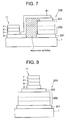
- the organic semiconductor diodes are island-shaped and formed electrically independently of the organic EL elements, but these two are electrically connected to each other by an electrode connection section 81 as shown in FIG. 7.
- This enables the organic semiconductor diodes 11 and the organic EL elements 200 connected in series to the organic semiconductor diodes 11 to be arranged together on the substrate.
- it is possible to form organic semiconductor diodes and organic EL elements together in a manner arranged in the form of an array.
- at least one of the hole transport layer and electron transport layer of the organic semiconductor diode can be formed of the same organic compound as that of at least one of the light-emitting layer and carrier transport layer of the organic EL element.
- the hole transport layer of the organic EL element and that of the organic semiconductor diode can be formed of a common compound.
- each organic EL element and each organic semiconductor diode can be arranged adjacent to each other, and configured in a manner such that they are laminated one upon the other.
- the area of an electrode of an organic semiconductor diode for forming an organic thin film diode on an organic EL element be minimized to reduce the capacity of the organic semiconductor diode, the area of the electrode is required to be large enough to prevent degradation of the rectifying action of the diode.
- the organic EL element display device by changing the film thickness of each layer of an organic EL element in each light-emitting portion, the film thickness of each layer of an organic semiconductor diode connected in series to the EL element, and the areas of the electrodes of the EL element and the diode, the organic semiconductor diode can be formed such that it has a smaller electrostatic capacity than that of the organic EL element. Therefore, it is possible to increase a light-emitting time period in one scanning by the amount of residual luminescence performed by electric charge emission corresponding to the capacity. Therefore, even if momentary brightness is reduced, sufficient luminescence brightness can be obtained to prevent deterioration of light-emitting portions. This makes it possible to increase the service life of a light-emitting panel.
- organic semiconductor diodes which can be manufactured by a low temperature process.
- a display panel can be produced by an organic thin film-laminating process alone. Since diode elements can be formed by organic thin films without using a silicon substrate, a large-sized full color display of an organic EL element display device based on the matrix driving method can be manufactured by a simple process for manufacturing an organic EL panel.
Landscapes
- Electroluminescent Light Sources (AREA)
Abstract
Description

















Claims (6)
- An organic semiconductor diode comprising:wherein said hole transport layer at an anode-side end has an ionization potential larger than an electron affinity of said electron transport layer at a cathode side end, whereby the organic semiconductor diode exhibiting nonlinear current-voltage characteristics when a voltage is applied between said hole transport layer and said electron transport layer in contact with each other.at least one hole transport layer which is arranged on an anode side and formed of an organic compound having a hole transport capability; andat least one electron transport layer which is arranged on a cathode side and formed of an organic compound having an electron transport capability, said at least one hole transport layer and said at least one electron transport layer being laminated one upon another,
- The organic semiconductor diode according to Claim 1, wherein as to all of two adjacent layers of said at least one hole transport layer, a hole transport layer on the anode side has a smaller ionization potential than that of another hole transport layer.
- The organic semiconductor diode according to Claim 1 or 2, wherein as to all of two adjacent layers of said at least one electron transport layer, an electron transport layer on the cathode side has a larger electron affinity than that of another electron transport layer.
- An organic electroluminescence element display device having plural light-emitting portions arranged in a display layout comprising:wherein each of said organic semiconductor diodes has a hole transport thin film layer which is arranged on an anode side and formed of an organic compound having a hole transport capability, and an electron transport thin film layer which is arranged on a cathode side and formed of an organic compound having an electron transport capability, the hole transport layer and the electron transport layer being laminated one upon another, said organic semiconductor diode exhibiting nonlinear current-voltage characteristics when a voltage is applied between the hole transport layer and the electron transport layer in contact with each other.a plurality of organic electroluminescence elements arranged therein as the light-emitting portions, said plurality of organic electroluminescence elements each including an anode, and a cathode, as well as a light-emitting layer having a light-emitting function and formed of an organic compound having at least an electron transport capability or a hole transport capability, and a carrier transport layer formed of an organic compound having at least a hole transport capability or an electron transport capability; andrespective organic semiconductor diodes each arranged adjacent to and at the same time connected in series to an associated one of said plurality of organic electroluminescence elements,
- The organic electroluminescence element display device according to Claim 4, wherein at least one of said hole transport layer and said electron transport layer of said organic semiconductor diode is formed of the same organic compound as that of at least one of said light-emitting layer and said carrier transport layer.
- The organic electroluminescence element display device according to Claim 4, wherein said organic semiconductor diode and said organic electroluminescence element are laminated one upon another.
Applications Claiming Priority (2)
| Application Number | Priority Date | Filing Date | Title |
|---|---|---|---|
| JP2001087133 | 2001-03-26 | ||
| JP2001087133A JP2002289355A (en) | 2001-03-26 | 2001-03-26 | Organic semiconductor diode and organic electroluminescent element display |
Publications (2)
| Publication Number | Publication Date |
|---|---|
| EP1251720A2 true EP1251720A2 (en) | 2002-10-23 |
| EP1251720A3 EP1251720A3 (en) | 2004-04-14 |
Family
ID=18942416
Family Applications (1)
| Application Number | Title | Priority Date | Filing Date |
|---|---|---|---|
| EP02252144A Withdrawn EP1251720A3 (en) | 2001-03-26 | 2002-03-25 | Organic semiconductor diode and organic electroluminescence element display device |
Country Status (3)
| Country | Link |
|---|---|
| US (1) | US6690028B2 (en) |
| EP (1) | EP1251720A3 (en) |
| JP (1) | JP2002289355A (en) |
Cited By (8)
| Publication number | Priority date | Publication date | Assignee | Title |
|---|---|---|---|---|
| FR2846794A1 (en) * | 2002-11-05 | 2004-05-07 | Thomson Licensing Sa | BI-STABLE ORGANIC ELECTROLUMINESCENT PANEL OR EACH CELL COMPRISES A SHOCKLEY DIODE |
| WO2004051750A1 (en) * | 2002-11-29 | 2004-06-17 | Siemens Aktiengesellschaft | Diode matrix for controlling displays with organic diodes and production method therefor |
| WO2006108514A3 (en) * | 2005-04-15 | 2007-04-05 | Polyic Gmbh & Co Kg | Multi-layer composite body having an electronic function |
| US7297621B2 (en) | 2003-04-15 | 2007-11-20 | California Institute Of Technology | Flexible carbon-based ohmic contacts for organic transistors |
| US7405775B2 (en) | 2003-01-17 | 2008-07-29 | Cbrite Inc. | Display employing organic material |
| US7898042B2 (en) | 2006-11-07 | 2011-03-01 | Cbrite Inc. | Two-terminal switching devices and their methods of fabrication |
| US8222077B2 (en) | 2006-11-07 | 2012-07-17 | Cbrite Inc. | Metal-insulator-metal (MIM) devices and their methods of fabrication |
| US9741901B2 (en) | 2006-11-07 | 2017-08-22 | Cbrite Inc. | Two-terminal electronic devices and their methods of fabrication |
Families Citing this family (20)
| Publication number | Priority date | Publication date | Assignee | Title |
|---|---|---|---|---|
| KR20020025918A (en) * | 2002-02-15 | 2002-04-04 | 박병주 | Organic semiconducting devices and organic electroluminescent devices produced by using wet process |
| JP2003303683A (en) * | 2002-04-09 | 2003-10-24 | Semiconductor Energy Lab Co Ltd | Luminous device |
| TW548859B (en) * | 2002-06-03 | 2003-08-21 | Ritdisplay Corp | Organic light-emitting display |
| JP2005026688A (en) * | 2003-06-30 | 2005-01-27 | Osram Opto Semiconductors Gmbh | Radiation emitting semiconductor chip, method for manufacturing the semiconductor chip, and method for adjusting and setting the brightness of the semiconductor chip |
| US7655961B2 (en) | 2003-10-02 | 2010-02-02 | Maxdem Incorporated | Organic diodes and materials |
| US7027044B2 (en) * | 2004-02-20 | 2006-04-11 | Au Optronics Corporation | Power line arrangement for electroluminescence display devices |
| DE102004029412A1 (en) * | 2004-02-27 | 2005-10-13 | Osram Opto Semiconductors Gmbh | Radiation-emitting semiconductor chip and method for producing such a semiconductor chip |
| JP4110417B2 (en) * | 2005-03-18 | 2008-07-02 | セイコーエプソン株式会社 | Surface emitting device and method for manufacturing the same |
| DE102005031448A1 (en) | 2005-07-04 | 2007-01-11 | Polyic Gmbh & Co. Kg | Activatable optical layer |
| TWI321968B (en) * | 2005-07-15 | 2010-03-11 | Lg Chemical Ltd | Organic light meitting device and method for manufacturing the same |
| DE102005035589A1 (en) | 2005-07-29 | 2007-02-01 | Polyic Gmbh & Co. Kg | Manufacturing electronic component on surface of substrate where component has two overlapping function layers |
| DE102005044306A1 (en) | 2005-09-16 | 2007-03-22 | Polyic Gmbh & Co. Kg | Electronic circuit and method for producing such |
| JP2007134629A (en) * | 2005-11-14 | 2007-05-31 | Konica Minolta Holdings Inc | Method for forming semiconductor layer, manufacturing apparatus for forming semiconductor layer |
| TW200809739A (en) * | 2006-08-08 | 2008-02-16 | Ritdisplay Corp | Method for fabricating active matrix organic electro-luminescence display panel |
| JP2012033918A (en) * | 2010-07-08 | 2012-02-16 | Mitsubishi Chemicals Corp | Organic electroluminescent element, organic electroluminescent device, organic el display device, and organic el lighting |
| WO2013125435A1 (en) * | 2012-02-20 | 2013-08-29 | 株式会社カネカ | Light emitting system and organic el apparatus |
| WO2014136359A1 (en) * | 2013-03-07 | 2014-09-12 | ローム株式会社 | Organic thin film solar cell, method for producing same, and electronic apparatus |
| KR102291895B1 (en) * | 2014-11-27 | 2021-08-20 | 엘지디스플레이 주식회사 | Indene carbonitrile composite and organic light emitting device comprising the same |
| TWI675472B (en) * | 2018-08-14 | 2019-10-21 | 友達光電股份有限公司 | Organic light emitting device and fabricating method thereof |
| WO2021144892A1 (en) * | 2020-01-15 | 2021-07-22 | シャープ株式会社 | Light-emitting element and light-emitting device |
Family Cites Families (8)
| Publication number | Priority date | Publication date | Assignee | Title |
|---|---|---|---|---|
| JP3534445B2 (en) * | 1993-09-09 | 2004-06-07 | 隆一 山本 | EL device using polythiophene |
| JP2821347B2 (en) * | 1993-10-12 | 1998-11-05 | 日本電気株式会社 | Current control type light emitting element array |
| JPH08330070A (en) * | 1995-05-29 | 1996-12-13 | Pioneer Electron Corp | Drive method for luminescent element |
| JP3281848B2 (en) * | 1996-11-29 | 2002-05-13 | 三洋電機株式会社 | Display device |
| US6004685A (en) * | 1997-12-23 | 1999-12-21 | Hewlett-Packard Company & The Board Of Regents Of The University Of Texas System | LED doped with periflanthene for efficient red emission |
| JP3466954B2 (en) * | 1998-04-24 | 2003-11-17 | キヤノン株式会社 | Light emitting diode device and method of manufacturing the same |
| US6350996B1 (en) * | 1998-04-24 | 2002-02-26 | Canon Kabushiki Kaisha | Light emitting diode device |
| US6366017B1 (en) * | 1999-07-14 | 2002-04-02 | Agilent Technologies, Inc/ | Organic light emitting diodes with distributed bragg reflector |
-
2001
- 2001-03-26 JP JP2001087133A patent/JP2002289355A/en not_active Abandoned
-
2002
- 2002-03-25 EP EP02252144A patent/EP1251720A3/en not_active Withdrawn
- 2002-03-25 US US10/104,048 patent/US6690028B2/en not_active Expired - Fee Related
Cited By (17)
| Publication number | Priority date | Publication date | Assignee | Title |
|---|---|---|---|---|
| EP1418567A1 (en) * | 2002-11-05 | 2004-05-12 | Thomson Licensing, Inc. | Bistable organic electroluminescent panel in which each cell includes a shockley diode |
| US7109956B2 (en) | 2002-11-05 | 2006-09-19 | Thomson Licensing | Bistable organic electroluminescent panel in which each cell includes a Shockley diode |
| FR2846794A1 (en) * | 2002-11-05 | 2004-05-07 | Thomson Licensing Sa | BI-STABLE ORGANIC ELECTROLUMINESCENT PANEL OR EACH CELL COMPRISES A SHOCKLEY DIODE |
| CN100448050C (en) * | 2002-11-05 | 2008-12-31 | 汤姆森许可贸易公司 | Bistable organic electroluminescent panels including Shockley diodes in each cell |
| WO2004051750A1 (en) * | 2002-11-29 | 2004-06-17 | Siemens Aktiengesellschaft | Diode matrix for controlling displays with organic diodes and production method therefor |
| US7528896B2 (en) | 2003-01-17 | 2009-05-05 | Cbrite, Inc. | Display employing organic material |
| US7405775B2 (en) | 2003-01-17 | 2008-07-29 | Cbrite Inc. | Display employing organic material |
| US8253910B2 (en) | 2003-01-17 | 2012-08-28 | Cbrite Inc. | Display employing organic material |
| US7297621B2 (en) | 2003-04-15 | 2007-11-20 | California Institute Of Technology | Flexible carbon-based ohmic contacts for organic transistors |
| WO2006108514A3 (en) * | 2005-04-15 | 2007-04-05 | Polyic Gmbh & Co Kg | Multi-layer composite body having an electronic function |
| US7812343B2 (en) | 2005-04-15 | 2010-10-12 | Polyic Gmbh & Co. Kg | Multilayer composite body having an electronic function |
| DE102005017655B4 (en) * | 2005-04-15 | 2008-12-11 | Polyic Gmbh & Co. Kg | Multilayer composite body with electronic function |
| CN101160594B (en) * | 2005-04-15 | 2014-03-05 | 波利Ic有限及两合公司 | Multilayer complexes with electronic functions |
| US7898042B2 (en) | 2006-11-07 | 2011-03-01 | Cbrite Inc. | Two-terminal switching devices and their methods of fabrication |
| US8193594B2 (en) | 2006-11-07 | 2012-06-05 | Cbrite Inc. | Two-terminal switching devices and their methods of fabrication |
| US8222077B2 (en) | 2006-11-07 | 2012-07-17 | Cbrite Inc. | Metal-insulator-metal (MIM) devices and their methods of fabrication |
| US9741901B2 (en) | 2006-11-07 | 2017-08-22 | Cbrite Inc. | Two-terminal electronic devices and their methods of fabrication |
Also Published As
| Publication number | Publication date |
|---|---|
| US6690028B2 (en) | 2004-02-10 |
| EP1251720A3 (en) | 2004-04-14 |
| US20030015805A1 (en) | 2003-01-23 |
| JP2002289355A (en) | 2002-10-04 |
Similar Documents
| Publication | Publication Date | Title |
|---|---|---|
| US6690028B2 (en) | Organic electroluminescence element display device with organic semiconductor diodes | |
| US6812638B2 (en) | Organic semiconductor diode | |
| US8735880B2 (en) | Light emitting transistor | |
| KR20020000875A (en) | Active organic el device and method of manufacture thereof | |
| CN1319184C (en) | Organic electroluminescence device | |
| CN1655210A (en) | Pixels for Active Matrix Displays | |
| JP2024110007A (en) | Organic light-emitting device, display device having the same, imaging device, lighting device, and mobile object | |
| JP7336277B2 (en) | Organic EL elements and display devices using the same, imaging devices, communication devices, lighting devices, lamps, mobile objects | |
| CN100346494C (en) | Organic electroluminescent device | |
| EP1246271A2 (en) | Organic semiconductor diode | |
| JP3820752B2 (en) | Organic electroluminescence device | |
| JP3555736B2 (en) | Organic electroluminescent device | |
| TWI292679B (en) | Storage capacitor in oled pixels and driving circuits and method for forming the same | |
| US6636001B2 (en) | Organic electronic device and nonlinear device | |
| KR100547055B1 (en) | Organic electroluminescent devices | |
| KR100572654B1 (en) | Organic electroluminescent devices | |
| KR100581639B1 (en) | Organic Electroluminescent Device | |
| JP4328704B2 (en) | Organic electroluminescence element and display device using the same | |
| JP2024108836A (en) | Organic light-emitting device, display device, imaging device, lighting device, mobile object | |
| JPH0982473A (en) | Organic electroluminescent device | |
| JP3852520B2 (en) | Organic electroluminescence device | |
| JPH09312196A (en) | EL device | |
| KR100581640B1 (en) | Organic Electroluminescent Device | |
| WO2020009039A1 (en) | Organic el element and display device, image pickup device, communication equipment, illumination device, lamp fitting, and mobile body using said organic el element |
Legal Events
| Date | Code | Title | Description |
|---|---|---|---|
| PUAI | Public reference made under article 153(3) epc to a published international application that has entered the european phase |
Free format text: ORIGINAL CODE: 0009012 |
|
| AK | Designated contracting states |
Kind code of ref document: A2 Designated state(s): AT BE CH CY DE DK ES FI FR GB GR IE IT LI LU MC NL PT SE TR |
|
| AX | Request for extension of the european patent |
Free format text: AL;LT;LV;MK;RO;SI |
|
| PUAL | Search report despatched |
Free format text: ORIGINAL CODE: 0009013 |
|
| AK | Designated contracting states |
Kind code of ref document: A3 Designated state(s): AT BE CH CY DE DK ES FI FR GB GR IE IT LI LU MC NL PT SE TR |
|
| AX | Request for extension of the european patent |
Extension state: AL LT LV MK RO SI |
|
| RIC1 | Information provided on ipc code assigned before grant |
Ipc: 7H 05B 33/08 A |
|
| 17P | Request for examination filed |
Effective date: 20040603 |
|
| AKX | Designation fees paid |
Designated state(s): DE FR GB |
|
| STAA | Information on the status of an ep patent application or granted ep patent |
Free format text: STATUS: THE APPLICATION IS DEEMED TO BE WITHDRAWN |
|
| 18D | Application deemed to be withdrawn |
Effective date: 20051206 |