EP1251563A2 - FET structures having symmetric and/or distributed feedforward capacitor connections - Google Patents
FET structures having symmetric and/or distributed feedforward capacitor connections Download PDFInfo
- Publication number
- EP1251563A2 EP1251563A2 EP02252759A EP02252759A EP1251563A2 EP 1251563 A2 EP1251563 A2 EP 1251563A2 EP 02252759 A EP02252759 A EP 02252759A EP 02252759 A EP02252759 A EP 02252759A EP 1251563 A2 EP1251563 A2 EP 1251563A2
- Authority
- EP
- European Patent Office
- Prior art keywords
- gate
- fingers
- fet
- serpentine
- capacitor
- Prior art date
- Legal status (The legal status is an assumption and is not a legal conclusion. Google has not performed a legal analysis and makes no representation as to the accuracy of the status listed.)
- Granted
Links
Images



Classifications
-
- H—ELECTRICITY
- H10—SEMICONDUCTOR DEVICES; ELECTRIC SOLID-STATE DEVICES NOT OTHERWISE PROVIDED FOR
- H10D—INORGANIC ELECTRIC SEMICONDUCTOR DEVICES
- H10D64/00—Electrodes of devices having potential barriers
- H10D64/20—Electrodes characterised by their shapes, relative sizes or dispositions
- H10D64/23—Electrodes carrying the current to be rectified, amplified, oscillated or switched, e.g. sources, drains, anodes or cathodes
- H10D64/251—Source or drain electrodes for field-effect devices
-
- H—ELECTRICITY
- H10—SEMICONDUCTOR DEVICES; ELECTRIC SOLID-STATE DEVICES NOT OTHERWISE PROVIDED FOR
- H10D—INORGANIC ELECTRIC SEMICONDUCTOR DEVICES
- H10D64/00—Electrodes of devices having potential barriers
- H10D64/20—Electrodes characterised by their shapes, relative sizes or dispositions
- H10D64/23—Electrodes carrying the current to be rectified, amplified, oscillated or switched, e.g. sources, drains, anodes or cathodes
- H10D64/251—Source or drain electrodes for field-effect devices
- H10D64/257—Source or drain electrodes for field-effect devices for lateral devices wherein the source or drain electrodes are characterised by top-view geometrical layouts, e.g. interdigitated, semi-circular, annular or L-shaped electrodes
-
- H—ELECTRICITY
- H10—SEMICONDUCTOR DEVICES; ELECTRIC SOLID-STATE DEVICES NOT OTHERWISE PROVIDED FOR
- H10D—INORGANIC ELECTRIC SEMICONDUCTOR DEVICES
- H10D64/00—Electrodes of devices having potential barriers
- H10D64/20—Electrodes characterised by their shapes, relative sizes or dispositions
- H10D64/27—Electrodes not carrying the current to be rectified, amplified, oscillated or switched, e.g. gates
- H10D64/311—Gate electrodes for field-effect devices
- H10D64/411—Gate electrodes for field-effect devices for FETs
-
- H—ELECTRICITY
- H10—SEMICONDUCTOR DEVICES; ELECTRIC SOLID-STATE DEVICES NOT OTHERWISE PROVIDED FOR
- H10D—INORGANIC ELECTRIC SEMICONDUCTOR DEVICES
- H10D84/00—Integrated devices formed in or on semiconductor substrates that comprise only semiconducting layers, e.g. on Si wafers or on GaAs-on-Si wafers
- H10D84/80—Integrated devices formed in or on semiconductor substrates that comprise only semiconducting layers, e.g. on Si wafers or on GaAs-on-Si wafers characterised by the integration of at least one component covered by groups H10D12/00 or H10D30/00, e.g. integration of IGFETs
- H10D84/811—Combinations of field-effect devices and one or more diodes, capacitors or resistors
-
- H—ELECTRICITY
- H10—SEMICONDUCTOR DEVICES; ELECTRIC SOLID-STATE DEVICES NOT OTHERWISE PROVIDED FOR
- H10D—INORGANIC ELECTRIC SEMICONDUCTOR DEVICES
- H10D84/00—Integrated devices formed in or on semiconductor substrates that comprise only semiconducting layers, e.g. on Si wafers or on GaAs-on-Si wafers
- H10D84/80—Integrated devices formed in or on semiconductor substrates that comprise only semiconducting layers, e.g. on Si wafers or on GaAs-on-Si wafers characterised by the integration of at least one component covered by groups H10D12/00 or H10D30/00, e.g. integration of IGFETs
- H10D84/811—Combinations of field-effect devices and one or more diodes, capacitors or resistors
- H10D84/813—Combinations of field-effect devices and capacitor only
Definitions
- the present invention relates to field effect transistor (FET) structures and, more particularly, to FET structures having symmetric and/or distributed feedforward capacitor connections.
- FET field effect transistor
- a feedforward capacitor with a low impedance can be used to improve the harmonic noise rejections of the FETs.
- signal distortions and noise interferences can be reduced or eliminated, and the performance of the FET structures can be improved greatly.
- a feedforward capacitor is connected between one side of a serpentine gate and the closest drain/source bar of a FET in a FET structure to improve the harmonic rejection characteristics of the FET structure.
- Figs. 1A and 1B of the accompanying drawings are top plan views of two different examples of such conventional serpentine FET structures having conventional feedforward capacitor connections.
- a conventional serpentine FET structure 5 or 7 includes a feedforward capacitor 18 and a FET 19 coupled with the feedforward capacitor 18.
- the feedforward capacitor 18 includes a bottom metal layer 10, a dielectric layer (not shown) disposed on the bottom metal layer 10, and a top metal layer 15 disposed on the dielectric layer.
- the FET 19 includes a drain manifold 14 having drain fingers 14a, a source manifold 16 having source fingers 16a, and a serpentine gate 12 serpentining between the drain and source fingers 14a and 16a.
- the top metal layer 15 is integrally connected to the drain manifold 14. That is, the top metal layer 15 functions as the drain manifold 14 of the FET 19 and as the top metal layer of the feedforward capacitor 18.
- the serpentine gate 12 of the FET 19 includes one end 12a directly connected to the bottom metal layer 10 of the feedforward capacitor 18, and the other end 12b indirectly connected to the feedforward capacitor 18 through the serpentining portion of the gate 12.
- FIG. 1B shows an alternative topology for an FET structure 7 in which the capacitor 18 and the FET 19 are not integrally connected.
- the capacitor is, however, electrically connected between the capacitor top plate 15 and the FET drain /source manifold 14.
- the gate 12 is connected at end 12a to the capacitor bottom plate 10.
- the series gate resistance encountered by the end 12b of the serpentine gate 12 reduces or cancels out the positive effect of the feedforward capacitor 18, such that the benefits of having the feedforward capacitor 18 in the FET structure cannot be effectively realized. Further, since the series gate resistance of the serpentine gate increases as the length of the serpentine gate increases, this problem becomes more significant in large FETs having long serpentine gates.
- the present invention provides FET structures which overcome the above-described problems and other problems associated with conventional FET structures.
- a bussed gate having gate fingers that are directly connected to a feedforward capacitor is used in the FET structure. This distributes evenly or symmetrically the capacitance of the feedforward capacitor to all the gate fingers, so that the effects of the feedforward capacitor can be realized throughout the gate fingers to improve the harmonic rejection characteristics of the FET.
- the present invention improves the harmonic noise rejections of the FET structure, the desired linearity in the FET structure can be easily achieved using low control voltages, thereby increasing the efficiency and effectiveness of the FET structure.
- the present invention provides a simple technique which effectively solves the problems encountered in prior art FET structures and which is particularly useful in large FET structures having lengthy serpentine gates.
- the present invention is directed to a structure comprising a FET including a gate having a plurality of gate fingers, a plurality of source fingers, and a plurality of drain fingers; and a feedforward capacitor integrally coupled with the FET for evenly or symmetrically distributing capacitance of the feedforward capacitor to the gate fingers.
- a 'direct connection' between two components means that there are no other components bridging the two components and that the two components are in contact with each other and extend directly from each other.
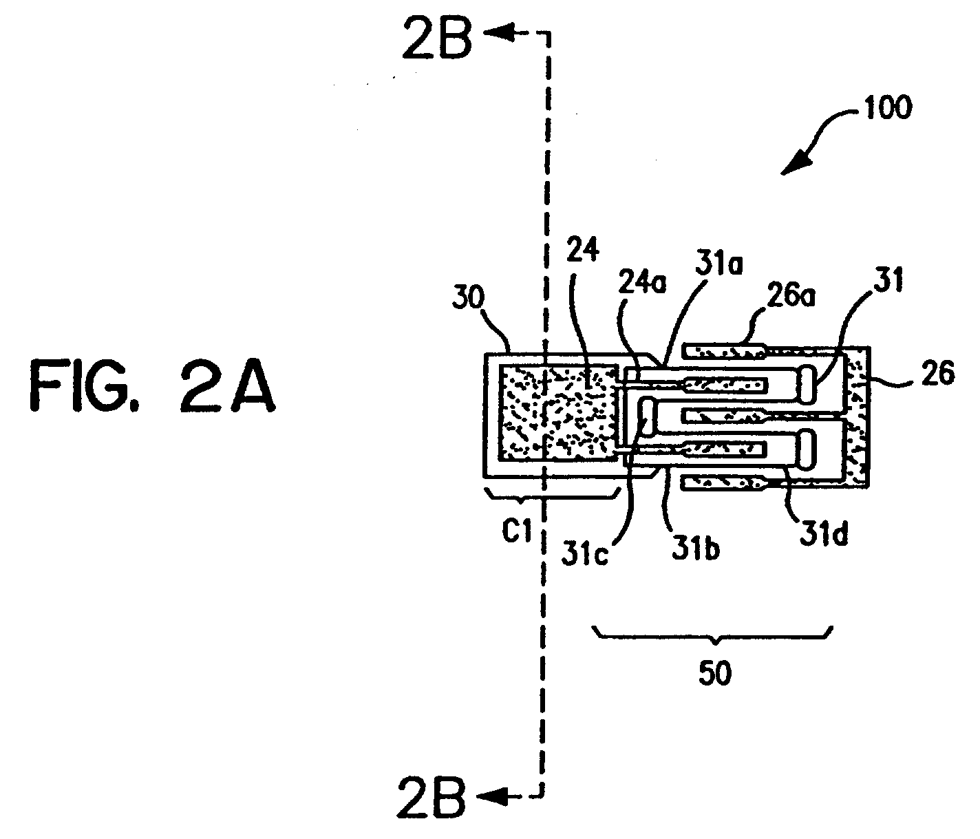
- a FET structure 100 includes a feedforward capacitor C1 and a serpentine FET 50 integrally coupled with the feedforward capacitor C1.
- the feedforward capacitor C1 includes a capacitor bottom metal layer 30, a dielectric layer 21 formed on the bottom metal layer 30, and a capacitor top metal layer 24 formed on the dielectric layer 21.
- the serpentine FET 50 includes the capacitor top metal layer 24 (or a portion thereof) functioning as a drain manifold for providing a plurality of drain fingers 24a, a source manifold 26 having a plurality of source fingers 26a, and a serpentine gate 31 having a plurality of gate fingers 31d serpentining between the drain and source fingers 24a and 26a.
- the serpentine gate 31 includes two end portions 31a and 31b which are directly connected to the bottom metal layer 30 of the feedforward capacitor C1, and a middle portion 31c which is not directly connected to any part of the feedforward capacitor C1.
- This direct and symmetrical connection of the serpentine gate 31 i.e., the direction connection of the end portions 31a and 31b to the metal layer 30
- This direct and symmetrical connection of the serpentine gate 31 i.e., the direction connection of the end portions 31a and 31b to the metal layer 30
- This direct and symmetrical connection of the serpentine gate 31 i.e., the direction connection of the end portions 31a and 31b to the metal layer 30
- This direct and symmetrical connection of the serpentine gate 31 i.e., the direction connection of the end portions 31a and 31b to the metal layer 30
- This direct and symmetrical connection of the serpentine gate 31 i.e., the direction connection of the end portions 31a and 31b to the metal layer 30
- the present invention improves greatly the performance of the FET structure. Furthermore, since the present invention improves the harmonic noise rejections of the FET structure, the desired linearity in the FET structure can be easily achieved using low control voltages, thereby increasing the efficiency and effectiveness of the FET structure.
- this second embodiment 102 of the FET structure includes a feedforward capacitor C1 and a serpentine FET 52 integrally coupled with the feedforward capacitor C1.
- the FET structure 102 is identical to the FET structure 100 of Fig. 2A, except that the middle portion 31C of the serpentine gate 31, as well as the two end portions 31a and 31b thereof, are connected directly to the bottom metal layer 30 of the feedforward capacitor C1. This results in all the gate fingers 31d of the serpentine gate 31 being directly connected to the bottom metal layer 30 of the feedforward capacitor C1.
- This configuration distributes evenly (i.e., in equal or approximately equal amount) and symmetrically the feedforward capacitance of the capacitor C1 across all the gate fingers 32a-31d of the serpentine gate 31, thereby improving significantly the performance characteristics of the FET structure 102.
- a FET structure 104 includes a feedforward capacitor C1 and a serpentine FET 54 integrally coupled with the feedforward capacitor C1.
- the FET structure 104 is identical to the FET structure 102 of Fig. 3, except that the two end portions 31a and 31b of the serpentine gate 31 are not directly connected to the bottom metal layer 30 of the feedforward capacitor C1. In other words, only the middle portion 31c of the serpentine gate 31 (and not the two end portions 31a and 31b of the serpentine gate 31) is connected directly to the feedforward capacitor C1. This results in the inner gate fingers 31d 2 and 31d 3 (and not the outer gate fingers 31d 1 and 31d 4 ) of the serpentine gate 31 to be in direct connection with the feedforward capacitor C1.
- the manner in which one side (i.e., the fingers 31d 1 and 31d 2 ) of the serpentine gate 31 is connected to the feedforward capacitor C1 is the same as the manner in which the other side (i.e., the fingers 31d 3 and 31d 4 ) of the serpentine gate 31 is connected to the feedforward capacitor C1.
- a symmetry in configuration exists between the two sides of the serpentine gate 31.
- This configuration symmetrically distributes the feedforward capacitance of the feedforward capacitor C1 to the gate fingers 31d of the serpentine gate 31, and thereby improves the performance characteristics of the FET structure 104.
- other portion(s) of the serpentine gate 31, except the two end portions 31a and 31b of the serpentine gate 31, can be connected directly to the feedforward capacitor C1 as long as this connection provides symmetry in the connection of the serpentine gate 31 to the feedforward capacitor C1.
- These configurations distribute symmetrically the feedforward capacitance of the capacitor C1 to the serpentine gate 31.
- a bussed FET having a bussed gate is used in the FET structure to connect with a feedforward capacitor.
- the FET structure 106 includes a feedforward capacitor C1 and a bussed FET 56 integrally coupled with the feedforward capacitor C1.
- the bussed FET 56 includes a source manifold 26 having source fingers 26a, a capacitor bottom metal layer/drain manifold 24 having drain fingers 24a, and a bussed gate 32 having bussed gate fingers 32a disposed between the drain and source fingers 24a and 26a. All the gate fingers 32a of the bussed gate 32 are directly connected to the bottom metal layer 30 of the feedforward capacitor C1. This allows the feedforward capacitance of the feedforward capacitor C1 to be evenly and symmetrically distributed across all the gate fingers 32a, which improves the performance of the FET structure 106 as discussed above.
- Fig. 6 is a top plan view of a cascaded FET structure 108 according to the present invention.
- the cascaded FET structure 108 includes first, second and third FET structures 100, 100' and 100" that are connected in series with each other.
- a source manifold 260 is used wherein the source manifold 260 has a plurality of first source fingers 260a extending in one direction and a plurality of second source fingers 260b extending in the opposite direction.
- a drain manifold 261 is used to connect the second FET structure 100' in series with the third FET structure 100".
- the drain manifold 261 has a plurality of first drain fingers 261a extending in one direction and a plurality of second drain fingers 261b extending in the opposite direction.
- the first FET structure 100 is identical to the FET structure shown in Fig. 2A and includes the feedforward capacitor C1 and the serpentine FET 50.
- the FET 50 includes a serpentine gate 31 having two end portions that are directly connected to the bottom metal layer 30 of the feedforward capacitor C1.
- the first source fingers 260a of the source manifold 260 function as the source fingers of the FET 50.
- the second FET structure 100' includes a second FET 50'.
- the second FET 50' includes the second source fingers 260b of the source manifold 260 as its source fingers, the second drain fingers 261b of the drain manifold 261 as its drain fingers, and a second serpentine gate 31' serpentining between the source and drain fingers 260b and 261b.
- the third FET structure 100" includes a third FET 50" and a second feedforward capacitor C2 integrally coupled with the third FET 50".
- the second feedforward capacitor C2 is identical to the first feedforward capacitor C1, except that its capacitor top metal layer 24' functions as the source manifold for providing source fingers 24a'.
- the third FET 50" includes the source manifold/top metal layer 24' having the source fingers 24a', the drain manifold 261 having the first drain fingers 261a, and a third serpentine gate 31". Both ends of the third serpentine gate 31" are connected directly to the bottom metal layer 30 of the second feedforward capacitor C2, which symmetrically distributes the feedforward capacitance of the feedforward capacitor C2 to the gate fingers of the third serpentine gate 31".
- the FET structure 100" is basically identical to the FET structure 100, except that the source and drain sides are switched.
- the two ends of the corresponding serpentine gate are connected directly to the feedforward capacitor C1 or C2 whereby the feedforward capacitance effects of the feedforward capacitors C1 and C2 are symmetrically applied to the corresponding serpentine gate, thereby greatly improving the performance of the cascaded FET structure 108.
- Fig. 7 is a top plan view of another embodiment of cascaded FET structure 110.
- the cascaded FET structure 110 is identical to the cascaded FET structure 108 shown in Fig. 6, except that bussed FETs are used in lieu of serpentine FETs on both sides of the cascaded connection.
- the cascaded FET structure 110 includes first, second and third FET structures 106, 106' and 106" that are connected in series with each other.
- the first FET structure 106 is identical to the FET structure shown in Fig. 5 and includes the feedforward capacitor C1 and the bussed FET 56.
- the FET 56 includes a first bussed gate 32 having bussed gate fingers directly connected to the bottom metal layer 30 of the feedforward capacitor C1.
- the first source fingers 260a of the source manifold 260 function as the source fingers of the FET 56.
- the second FET structure 106' is identical to the second FET structure 100' in Fig. 6, and includes a second FET 56' having a serpentine gate 31', second source fingers 260b, and second drain fingers 261b.
- the third FET structure 106" includes a third FET 56" and a second feedforward capacitor C2 integrally coupled with the third FET 56".
- the third FET 56" includes a source manifold 24' having source fingers 24a', a drain manifold 261 having first drain fingers 261a, and a bussed gate 32". All the gate fingers of the bussed gate 32" are connected directly to the bottom metal layer 30 of the second feedforward capacitor C2, which symmetrically and evenly distributes the feedforward capacitance of the feedforward capacitor C2 to the gate fingers of the bussed gate 32".
- the third FET structure 106" is basically identical to the first FET structure 106, except that the source and drain sides are switched.
- the FET structures 100 and 100" of the cascaded FET structure 108 shown in Fig. 6 can be substituted with other FET structures such as the FET structure 102 or 104 shown in Figs 3 and 4.
- the FET structures 100 and 100" can be replaced with two FET structures 102 or two FET structures 104.
- a mixed combination of the FET structures 100, 102, 104 and 106 may be used in one cascaded FET structure. In all these embodiments, any number of FET structures can be cascaded to produce a cascaded FET structure.
- Fig. 8 is a schematic circuit diagram of the cascaded FET structure 108 or 110 shown in Fig. 6 or 7.
- This circuit diagram clearly indicates that, in the cascaded FET structure 108, the serpentine gates 31, 31' and 31" respectively correspond to the gates G1, G2 and G3 in the circuit diagram.
- the FETs 50, 50' and 50" respectively correspond to the FETs FET1, FET2, and FET3.
- the bussed gate 32, the serpentine gate 31' and the bussed gate 32" respectively correspond to the gates G1, G2 and G3 in the circuit diagram.
- the FETs 56, 56' and 56" respectively correspond to the FETs FET1, FET2, and FET3.
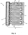
- Fig. 9 is a top plan view of a multi-gate FET structure 112. As shown, it includes a feedforward capacitor C1 and a multi-gate FET 57 integrally coupled with the feedforward capacitor C1. As discussed above, the feedforward capacitor C1 includes a capacitor bottom metal layer 30, a capacitor top metal layer/drain manifold 24, and a dielectric layer 21 (Fig. 2B) disposed between the layers 24 and 30.
- the multi-gate FET 57 includes the drain manifold 24 having drain fingers 24a, a source manifold 26 having source fingers 26a, a bussed gate having bussed gate fingers 32a directly connected to the capacitor bottom metal layer 30, and a serpentine gate 33 having serpentine gate fingers 33a.
- the serpentine gate 33 serpentines between the gate fingers 32a and the drain or source fingers 24a or 26a. There exists one bussed gate finger 32a and one serpentine gate finger 33a between each drain finger 24a and an adjacent source finger 26a. Since all the gate fingers 32a are directly connected to the bottom metal layer 30 of the feedforward capacitor C1, the feedforward capacitance of the capacitor C1 is evenly and symmetrically distributed to the gate fingers 32a of the gate 32, thereby improving the performance of the FET structure 112.
- Fig. 10 is a top plan view of a multi-gate FET structure 114 which is identical to the multi-gate FET structure 112 of Figure 9, except that the multi-gate FET structure 114 includes an additional serpentine gate 34. More specifically, as shown, the multi-gate FET structure 114 includes a feedforward capacitor C1 and a multi-gate FET 58 integrally coupled with the feedforward capacitor C1.
- the multi-gate FET 58 includes a drain manifold 24 having drain fingers 24a, a source manifold 26 having source fingers 26a, a bussed gate 32 having bussed gate fingers 32a directly connected to the capacitor bottom metal layer 30 of the capacitor C1, a first serpentine gate 33, and a second serpentine gate 34.
- the first and second serpentine gates 33 and 34 serpentine between the bussed gate fingers 32a and the drain or source fingers 24a or 26a.
- the direct connection of all the bussed gate fingers 32a to the bottom metal layer 30 of the feedforward capacitor C1 evenly and symmetrically distributes the feedforward capacitance of the capacitor C1 to the gate fingers 32a. This improves the performance characteristics of the FET structure 114.
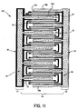
- Fig. 11 is a top plan view of a multi-gate FET structure 116 in which two bussed gates and a serpentine gate are provided.
- the multi-gate FET structure 116 includes first and second feedforward capacitors C1 and C3 and a multi-gate FET 59 integrally coupled with the feedforward capacitors C1 and C3.
- the first feedforward capacitor C1 includes a first capacitor bottom metal layer 30, a first capacitor top metal layer/drain manifold 24, and a first dielectric layer disposed between the layers 24 and 30.
- the second feedforward capacitor C3 includes a second capacitor bottom metal layer 27, a second capacitor top metal layer/source manifold 26, and a second dielectric layer disposed between the layers 26 and 27.
- the multi-gate FET 59 includes the drain manifold 24 having drain fingers 24a, the source manifold 26 having source fingers 26a, a first bussed gate 32 having first bussed gate fingers 32a directly connected to the first capacitor bottom metal layer 30, a second bussed gate 29 having second bussed gate fingers 29a directly connected to the second capacitor bottom metal layer 27, and at least one serpentine gate 33.
- the serpentine gate 33 serpentines between the bussed gate fingers 32a and 29a.
- the feedforward capacitor connection of the present invention is applicable to any FET structures and other electronic devices which require the use of feedforward capacitor(s). Such variations are contemplated as part of the present invention.
- the drain and source are interchangeable due to the symmetric placement of gates within a channel.
- the layouts provided in these embodiments can be modified and scaled to include any number of serpentine gates, serpentine gate fingers, bussed gates, bussed gate fingers, drain fingers, source fingers, drain manifolds, source manifolds, feedforward capacitors, and/or cascaded FET structures as well as any width, length, thickness, size, shape and/or configuration for any component of the FET structures.
- these layouts can be modified and scaled to handle any FET device periphery and capacitor combination.
- the bottom layer of the capacitor be the same structure as the gate manifold or that the top layer of the capacitor be the drain/source manifold of the FET.
Landscapes
- Junction Field-Effect Transistors (AREA)
- Semiconductor Integrated Circuits (AREA)
- Metal-Oxide And Bipolar Metal-Oxide Semiconductor Integrated Circuits (AREA)
- Insulated Gate Type Field-Effect Transistor (AREA)
Abstract
Description
Claims (24)
- A structure comprising a field effect transistor (FET) (50) including a gate (31) having a plurality of gate fingers (31a-31d), a plurality of source fingers (26a) and a plurality of drain fingers (24a) and a feedforward capacitor (C1), characterised in that the feed forward capacitor (C1) is coupled with the FET (50) for evenly or symmetrically distributing capacitance of the feedforward capacitor to the gate fingers (31a-31c).
- The structure of claim 1, wherein the gate is a serpentine gate (31) serpentining between the source and drain fingers (26a,24a), and includes first and second ends (31a,31b) connected directly to the feedforward capacitor.
- The structure of claim 2, wherein the serpentine gate (31) includes a middle portion that is not connected directly to the feedforward capacitor (C1).
- The structure of claim 2, wherein the serpentine gate (31) includes a middle portion that is also connected directly to the feedforward capacitor (C1).
- The structure of claim 2, wherein the serpentine gate (31) includes evenly distributed portions (31d2,31d3) second ends, said evenly distributed portions being directly connected to the feedforward capacitor.
- The structure of claim 1, wherein the gate is a serpentine gate (31) serpentining between the source and drain fingers, and includes first and second ends (21a,31b) and at least one portion (31c) between the first and second ends, wherein said at least one portion and not the first and second ends is connected directly to the feedforward capacitor (C1).
- The structure of claim 6, wherein said at least one portion (31c) of the serpentine gate is a middle portion of the serpentine gate, or evenly distributed portions disposed between the first and second ends of the serpentine gate.
- The structure of claim 1, wherein the gate is a bussed gate (32) and each of the plurality of gate fingers (32a) is connected directly to the feedforward capacitor (C1).
- The structure of any preceding claim, wherein the feedforward capacitor (C1) includes a bottom conductive layer (30), a top conductive layer (24), and a dielectric layer (21) disposed between the top and bottom conductive layers.
- The structure of claim 9, wherein the gate fingers extend from the bottom conductive layer (30) of the feedforward capacitor (C1), and the drain or source fingers extend from the top conductive layer (24) of the feedforward capacitor.
- The structure (108) of claim 1, further comprising:a second FET 50")including a second gate (31") having a plurality of second gate fingers, a plurality of second source fingers (24a'), and a plurality of second drain fingers (261a);a second feedforward capacitor (C2) coupled with the second FET for evenly or symmetrically distributing capacitance of the second feedforward capacitor to the second gate fingers; andat least one third FET (50') connected between the first and second FETs (50,50") and including a third gate (31') having a plurality of third gate fingers, a plurality of third source fingers (260b), and a plurality of third drain fingers (261b).
- The structure of claim 11, wherein at least one of the first and second gates (31,31") is a serpentine gate having first and second ends, the first and second ends of the serpentine gate being connected directly to the first or second feedforward capacitor (C1,C2).
- The structure of claim 12, wherein the third gate (31) is a serpentine gate, and the first, second and third FETs are connected in series with each other.
- The structure of claim 13, wherein the serpentine gate (31') includes a middle portion that is not connected directly to the first or second feedforward capacitor.
- The structure of claim 13, wherein the serpentine gate (31') includes a middle portion that is connected directly to the first or second feedforward capacitor (C1,C2).
- The structure of claim 13, wherein the serpentine gate (31') includes evenly distributed portions between the first and second ends, said evenly distributed portions being directly connected to the feedforward capacitor.
- The structure of any preceding claim 11 to 16, wherein at least one of the first and second gates (31,31") is a serpentine gate having first and second ends and at least one portion between the first and second ends, wherein said at least one portion and not the first and second ends is connected directly to the first or second feedforward capacitor (C1,C2).
- The structure of claim 17, wherein said at least one portion of the serpentine gate (31,31") is a middle portion of the serpentine gate, or evenly-distributed portions disposed between the first and second ends of the serpentine gate.
- The structure (110) of any preceding claim 11 to 16, wherein at least one of the first and second gates (32,32") is a bussed gate having a plurality of bussed gate fingers that are connected directly to the first or second feedforward capacitor (C1,C2).
- The structure (112,114,116) of claim 1, wherein:the gate is a bussed gate (32) having the plurality of gate fingers (32a) connected directly to the feedforward capacitor (C1), andwherein the structure includes at least one second gate (33) having a plurality of second gate fingers serpentining between the source and drain fingers of the FET (57,58,59).
- The structure (116) of claim 20, wherein the feedforward capacitor (C1) is connected directly to a first side of the FET (59), and wherein the structure includes:a third gate (29) having a plurality of third gate fingers; anda second feedforward capacitor (C3) coupled to a second side of the FET (59) for evenly or symmetrically distributing capacitance of the second feedforward capacitor to the third gate fingers.
- The structure of claim 21, wherein the second and third gates are bussed gates having bussed gate fingers.
- The structure of claim 21, wherein the first and second sides of the FET are drain and source sides respectively, or source and drain sides respectively.
- The structure of claim 23, wherein one gate finger of the first gate (32), one gate finger of each of said at least one second gate (33), and one gate finger of the third gate (29) are disposed between one of the source fingers (26a) and one of the drain fingers (24a) of the FET (59).
Applications Claiming Priority (4)
| Application Number | Priority Date | Filing Date | Title |
|---|---|---|---|
| US28454601P | 2001-04-18 | 2001-04-18 | |
| US284546P | 2001-04-18 | ||
| US966189 | 2001-09-28 | ||
| US09/966,189 US6426525B1 (en) | 2001-04-18 | 2001-09-28 | FET structures having symmetric and/or distributed feedforward capacitor connections |
Publications (3)
| Publication Number | Publication Date |
|---|---|
| EP1251563A2 true EP1251563A2 (en) | 2002-10-23 |
| EP1251563A3 EP1251563A3 (en) | 2007-01-03 |
| EP1251563B1 EP1251563B1 (en) | 2009-06-24 |
Family
ID=26962671
Family Applications (1)
| Application Number | Title | Priority Date | Filing Date |
|---|---|---|---|
| EP02252759A Expired - Lifetime EP1251563B1 (en) | 2001-04-18 | 2002-04-18 | FET structures having symmetric and/or distributed feedforward capacitor connections |
Country Status (4)
| Country | Link |
|---|---|
| US (1) | US6426525B1 (en) |
| EP (1) | EP1251563B1 (en) |
| JP (1) | JP2002373986A (en) |
| DE (1) | DE60232699D1 (en) |
Cited By (2)
| Publication number | Priority date | Publication date | Assignee | Title |
|---|---|---|---|---|
| GB2439820B (en) * | 2006-06-28 | 2011-06-01 | Filtronic Compound Semiconductors Ltd | A field effect transistor and a linear antenna switch arm |
| CN112750814A (en) * | 2019-10-31 | 2021-05-04 | 英飞凌科技奥地利有限公司 | Semiconductor device and inverter |
Families Citing this family (22)
| Publication number | Priority date | Publication date | Assignee | Title |
|---|---|---|---|---|
| CN100366179C (en) * | 2002-05-21 | 2008-02-06 | 荷兰联合利华有限公司 | Frozen aerated product in a container |
| US6730953B2 (en) * | 2002-09-13 | 2004-05-04 | Mia-Com, Inc. | Apparatus, methods and articles of manufacture for a low control voltage switch |
| US6803680B2 (en) * | 2002-09-13 | 2004-10-12 | Mia-Com, Inc. | Apparatus, methods, and articles of manufacture for a switch having sharpened control voltage |
| US7250804B2 (en) * | 2002-12-17 | 2007-07-31 | M/A -Com, Inc. | Series/shunt switch and method of control |
| US7030515B2 (en) | 2003-05-21 | 2006-04-18 | M/A-Com, Inc. | Individually biased transistor high frequency switch |
| US20050116257A1 (en) * | 2003-06-20 | 2005-06-02 | James Oakes | Field effect transister structures |
| JP4380264B2 (en) * | 2003-08-25 | 2009-12-09 | カシオ計算機株式会社 | Bonding substrate and substrate bonding method |
| US20060237750A1 (en) * | 2004-06-21 | 2006-10-26 | James Oakes | Field effect transistor structures |
| GB2475645B (en) * | 2006-06-28 | 2011-10-26 | Rfmd | A field effect transistor |
| JP2009231583A (en) * | 2008-03-24 | 2009-10-08 | Sanyo Electric Co Ltd | Compound semiconductor switch circuit device |
| JP5397289B2 (en) * | 2010-03-29 | 2014-01-22 | 住友電気工業株式会社 | Field effect transistor |
| JP2012028977A (en) * | 2010-07-22 | 2012-02-09 | New Japan Radio Co Ltd | Field-effect transistor with additional capacitance and semiconductor switch circuit |
| JP2015207576A (en) * | 2014-04-17 | 2015-11-19 | ソニー株式会社 | Semiconductor device, antenna switch circuit, and radio communication device |
| US11670605B2 (en) * | 2020-04-03 | 2023-06-06 | Wolfspeed, Inc. | RF amplifier devices including interconnect structures and methods of manufacturing |
| US11837457B2 (en) | 2020-09-11 | 2023-12-05 | Wolfspeed, Inc. | Packaging for RF transistor amplifiers |
| US11356070B2 (en) | 2020-06-01 | 2022-06-07 | Wolfspeed, Inc. | RF amplifiers having shielded transmission line structures |
| US12647083B2 (en) | 2020-04-03 | 2026-06-02 | Wolfspeed, Inc. | RF amplifier devices and methods of manufacturing including modularized designs with flip chip interconnections and integration into packaging |
| US12166003B2 (en) | 2020-04-03 | 2024-12-10 | Macom Technology Solutions Holdings, Inc. | RF amplifier devices including top side contacts and methods of manufacturing |
| US12500562B2 (en) | 2020-04-03 | 2025-12-16 | Macom Technology Solutions Holdings, Inc. | RF amplifier devices and methods of manufacturing including modularized designs with flip chip interconnections |
| CN114335167A (en) * | 2021-12-22 | 2022-04-12 | 深圳市千屹芯科技有限公司 | SiC JFET device for radio frequency field and radio frequency device |
| US12620530B2 (en) | 2022-09-23 | 2026-05-05 | Wolfspeed, Inc. | Device and process for implementing silicon carbide (SiC) surface mount devices |
| EP4343831A1 (en) * | 2022-09-25 | 2024-03-27 | Wolfspeed, Inc. | Field effect transistor with integrated series capacitance |
Family Cites Families (12)
| Publication number | Priority date | Publication date | Assignee | Title |
|---|---|---|---|---|
| JPS5944848A (en) * | 1982-09-06 | 1984-03-13 | Nec Corp | High frequency high output transistor |
| US4725747A (en) * | 1986-08-29 | 1988-02-16 | Texas Instruments Incorporated | Integrated circuit distributed geometry to reduce switching noise |
| JPS6377165A (en) * | 1986-09-19 | 1988-04-07 | Mitsubishi Electric Corp | Semiconductor device |
| JP2594558B2 (en) * | 1987-04-30 | 1997-03-26 | 日本電気株式会社 | Field-effect transistor |
| US4786881A (en) * | 1987-08-27 | 1988-11-22 | General Electric Company | Amplifier with integrated feedback network |
| US4949139A (en) * | 1988-09-09 | 1990-08-14 | Atmel Corporation | Transistor construction for low noise output driver |
| US6285070B1 (en) * | 1995-12-22 | 2001-09-04 | Micron Technology, Inc. | Method of forming semiconductor die with integral decoupling capacitor |
| US6002156A (en) * | 1997-09-16 | 1999-12-14 | Winbond Electronics Corp. | Distributed MOSFET structure with enclosed gate for improved transistor size/layout area ratio and uniform ESD triggering |
| US5955763A (en) * | 1997-09-16 | 1999-09-21 | Winbond Electronics Corp. | Low noise, high current-drive MOSFET structure for uniform serpentine-shaped poly-gate turn-on during an ESD event |
| JPH11122054A (en) * | 1997-10-14 | 1999-04-30 | Toshiba Corp | Monolithic microwave amplifier |
| JPH11251584A (en) * | 1998-03-03 | 1999-09-17 | Matsushita Electron Corp | Transistor and high frequency amplifier using the same |
| JP3373435B2 (en) * | 1998-06-25 | 2003-02-04 | 日本電信電話株式会社 | Resistive feedback transistor |
-
2001
- 2001-09-28 US US09/966,189 patent/US6426525B1/en not_active Expired - Lifetime
-
2002
- 2002-04-18 DE DE60232699T patent/DE60232699D1/en not_active Expired - Lifetime
- 2002-04-18 JP JP2002116248A patent/JP2002373986A/en active Pending
- 2002-04-18 EP EP02252759A patent/EP1251563B1/en not_active Expired - Lifetime
Cited By (5)
| Publication number | Priority date | Publication date | Assignee | Title |
|---|---|---|---|---|
| GB2439820B (en) * | 2006-06-28 | 2011-06-01 | Filtronic Compound Semiconductors Ltd | A field effect transistor and a linear antenna switch arm |
| CN112750814A (en) * | 2019-10-31 | 2021-05-04 | 英飞凌科技奥地利有限公司 | Semiconductor device and inverter |
| EP4333304A3 (en) * | 2019-10-31 | 2024-06-05 | Infineon Technologies Austria AG | Semiconductor device and inverter |
| US12068379B2 (en) | 2019-10-31 | 2024-08-20 | Infineon Technologies Austria Ag | Semiconductor device having a lateral transistor device and an inverter that includes the semiconductor device |
| CN112750814B (en) * | 2019-10-31 | 2025-11-18 | 英飞凌科技奥地利有限公司 | Semiconductor devices and inverters |
Also Published As
| Publication number | Publication date |
|---|---|
| EP1251563B1 (en) | 2009-06-24 |
| EP1251563A3 (en) | 2007-01-03 |
| JP2002373986A (en) | 2002-12-26 |
| US6426525B1 (en) | 2002-07-30 |
| DE60232699D1 (en) | 2009-08-06 |
Similar Documents
| Publication | Publication Date | Title |
|---|---|---|
| EP1251563B1 (en) | FET structures having symmetric and/or distributed feedforward capacitor connections | |
| JP4800084B2 (en) | Semiconductor device and manufacturing method thereof | |
| US11139373B2 (en) | Scalable circuit-under-pad device topologies for lateral GaN power transistors | |
| DE19939933B4 (en) | Electronic power module unit | |
| US5883407A (en) | Semiconductor device | |
| JP7072118B1 (en) | Digital phase shift circuit and digital phase shifter | |
| JP3144477B2 (en) | Switch circuit and semiconductor device | |
| US5973377A (en) | Semiconductor device having FETs with shared source and drain regions | |
| KR20000057854A (en) | Insulated gate transistor | |
| DE102009030965A1 (en) | Semiconductor structure, has gate electrode insulated with body regions, and power transistor connected with snubber capacitor and snubber resistance, where power transistor is extended within silicon region | |
| KR960026768A (en) | Insulated Gate Semiconductor Device | |
| JP4908006B2 (en) | Semiconductor device | |
| US10903834B1 (en) | Power electronic device with paralleled transistors | |
| JP4245726B2 (en) | Millimeter-wave band semiconductor switch circuit | |
| JP2005183770A (en) | High frequency semiconductor devices | |
| US20210367035A1 (en) | SCALABLE CIRCUIT-UNDER-PAD DEVICE TOPOLOGIES FOR LATERAL GaN POWER TRANSISTORS | |
| DE112021002273T5 (en) | SEMICONDUCTOR COMPONENT | |
| KR100211030B1 (en) | Insulator device with built-in MOS transistor using multilayer metallization technology | |
| JP2004320040A (en) | MOS transistor having a mesh type gate electrode | |
| CN103456713B (en) | Switching circuit | |
| JPH088441A (en) | Dual gate type field effect transistor | |
| JP2006269835A (en) | Semiconductor device | |
| WO2015101973A1 (en) | Semiconductor device | |
| DE112022003874T5 (en) | SEMICONDUCTOR COMPONENT AND MOUNTING STRUCTURE FOR THE SEMICONDUCTOR COMPONENT | |
| US5311156A (en) | High frequency double pole double throw switch |
Legal Events
| Date | Code | Title | Description |
|---|---|---|---|
| PUAI | Public reference made under article 153(3) epc to a published international application that has entered the european phase |
Free format text: ORIGINAL CODE: 0009012 |
|
| AK | Designated contracting states |
Kind code of ref document: A2 Designated state(s): AT BE CH CY DE DK ES FI FR GB GR IE IT LI LU MC NL PT SE TR |
|
| AX | Request for extension of the european patent |
Free format text: AL;LT;LV;MK;RO;SI |
|
| PUAL | Search report despatched |
Free format text: ORIGINAL CODE: 0009013 |
|
| AK | Designated contracting states |
Kind code of ref document: A3 Designated state(s): AT BE CH CY DE DK ES FI FR GB GR IE IT LI LU MC NL PT SE TR |
|
| AX | Request for extension of the european patent |
Extension state: AL LT LV MK RO SI |
|
| 17P | Request for examination filed |
Effective date: 20070621 |
|
| AKX | Designation fees paid |
Designated state(s): DE FR GB |
|
| 17Q | First examination report despatched |
Effective date: 20070831 |
|
| GRAP | Despatch of communication of intention to grant a patent |
Free format text: ORIGINAL CODE: EPIDOSNIGR1 |
|
| RAP1 | Party data changed (applicant data changed or rights of an application transferred) |
Owner name: COBHAM DEFENSE ELECTRONIC SYSTEMS CORPORATION |
|
| GRAS | Grant fee paid |
Free format text: ORIGINAL CODE: EPIDOSNIGR3 |
|
| GRAA | (expected) grant |
Free format text: ORIGINAL CODE: 0009210 |
|
| AK | Designated contracting states |
Kind code of ref document: B1 Designated state(s): DE FR GB |
|
| REG | Reference to a national code |
Ref country code: GB Ref legal event code: FG4D |
|
| REF | Corresponds to: |
Ref document number: 60232699 Country of ref document: DE Date of ref document: 20090806 Kind code of ref document: P |
|
| REG | Reference to a national code |
Ref country code: GB Ref legal event code: 732E Free format text: REGISTERED BETWEEN 20100114 AND 20100120 |
|
| RAP2 | Party data changed (patent owner data changed or rights of a patent transferred) |
Owner name: M/A-COM TECHNOLOGY SOLUTIONS HOLDINGS, INC. |
|
| PLBE | No opposition filed within time limit |
Free format text: ORIGINAL CODE: 0009261 |
|
| STAA | Information on the status of an ep patent application or granted ep patent |
Free format text: STATUS: NO OPPOSITION FILED WITHIN TIME LIMIT |
|
| 26N | No opposition filed |
Effective date: 20100325 |
|
| REG | Reference to a national code |
Ref country code: FR Ref legal event code: PLFP Year of fee payment: 15 |
|
| REG | Reference to a national code |
Ref country code: FR Ref legal event code: PLFP Year of fee payment: 16 |
|
| REG | Reference to a national code |
Ref country code: FR Ref legal event code: PLFP Year of fee payment: 17 |
|
| PGFP | Annual fee paid to national office [announced via postgrant information from national office to epo] |
Ref country code: FR Payment date: 20210423 Year of fee payment: 20 Ref country code: DE Payment date: 20210420 Year of fee payment: 20 |
|
| PGFP | Annual fee paid to national office [announced via postgrant information from national office to epo] |
Ref country code: GB Payment date: 20210421 Year of fee payment: 20 |
|
| REG | Reference to a national code |
Ref country code: DE Ref legal event code: R071 Ref document number: 60232699 Country of ref document: DE |
|
| REG | Reference to a national code |
Ref country code: GB Ref legal event code: PE20 Expiry date: 20220417 |
|
| PG25 | Lapsed in a contracting state [announced via postgrant information from national office to epo] |
Ref country code: GB Free format text: LAPSE BECAUSE OF EXPIRATION OF PROTECTION Effective date: 20220417 |