EP1251560A1 - Cluster globular semiconductor device - Google Patents

Cluster globular semiconductor device Download PDF

Info

Publication number
EP1251560A1
EP1251560A1 EP01958486A EP01958486A EP1251560A1 EP 1251560 A1 EP1251560 A1 EP 1251560A1 EP 01958486 A EP01958486 A EP 01958486A EP 01958486 A EP01958486 A EP 01958486A EP 1251560 A1 EP1251560 A1 EP 1251560A1
Authority
EP
European Patent Office
Prior art keywords
spherical
cluster
semiconductors
semiconductor device
spherical semiconductors
Prior art date
Legal status (The legal status is an assumption and is not a legal conclusion. Google has not performed a legal analysis and makes no representation as to the accuracy of the status listed.)
Withdrawn
Application number
EP01958486A
Other languages
German (de)
French (fr)
Other versions
EP1251560A4 (en
Inventor
Yoshito Abe
Current Assignee (The listed assignees may be inaccurate. Google has not performed a legal analysis and makes no representation or warranty as to the accuracy of the list.)
Dai Nippon Printing Co Ltd
Original Assignee
Dai Nippon Printing Co Ltd
Priority date (The priority date is an assumption and is not a legal conclusion. Google has not performed a legal analysis and makes no representation as to the accuracy of the date listed.)
Filing date
Publication date
Application filed by Dai Nippon Printing Co Ltd filed Critical Dai Nippon Printing Co Ltd
Publication of EP1251560A1 publication Critical patent/EP1251560A1/en
Publication of EP1251560A4 publication Critical patent/EP1251560A4/en
Withdrawn legal-status Critical Current

Links

Images

Classifications

    • H—ELECTRICITY
    • H10—SEMICONDUCTOR DEVICES; ELECTRIC SOLID-STATE DEVICES NOT OTHERWISE PROVIDED FOR
    • H10W—GENERIC PACKAGES, INTERCONNECTIONS, CONNECTORS OR OTHER CONSTRUCTIONAL DETAILS OF DEVICES COVERED BY CLASS H10
    • H10W90/00—Package configurations
    • H—ELECTRICITY
    • H10—SEMICONDUCTOR DEVICES; ELECTRIC SOLID-STATE DEVICES NOT OTHERWISE PROVIDED FOR
    • H10D—INORGANIC ELECTRIC SEMICONDUCTOR DEVICES
    • H10D62/00—Semiconductor bodies, or regions thereof, of devices having potential barriers
    • H10D62/10—Shapes, relative sizes or dispositions of the regions of the semiconductor bodies; Shapes of the semiconductor bodies
    • H10D62/117—Shapes of semiconductor bodies
    • H—ELECTRICITY
    • H10—SEMICONDUCTOR DEVICES; ELECTRIC SOLID-STATE DEVICES NOT OTHERWISE PROVIDED FOR
    • H10W—GENERIC PACKAGES, INTERCONNECTIONS, CONNECTORS OR OTHER CONSTRUCTIONAL DETAILS OF DEVICES COVERED BY CLASS H10
    • H10W90/00—Package configurations
    • H10W90/701—Package configurations characterised by the relative positions of pads or connectors relative to package parts
    • H10W90/721—Package configurations characterised by the relative positions of pads or connectors relative to package parts of bump connectors
    • H10W90/722—Package configurations characterised by the relative positions of pads or connectors relative to package parts of bump connectors between stacked chips

Definitions

  • the present invention relates to a cluster spherical semiconductor device having a plurality of spherical semiconductors cluster-connected to each other.
  • a three-dimensional arrangement of a spherical semiconductor in a conventionally proposed cluster spherical semiconductor device is a simple tetragonal cubic lattice.
  • Fig. 4(A) shows a perspective view of this arrangement.
  • a cluster spherical semiconductor device 42 requires an electrode for electrically connecting a plurality of spherical semiconductors 41a, 41b to each other, or for connecting the spherical semiconductors 41a, 41b to another semiconductor device or a substrate.
  • an electrode is provided in the conventionally proposed spherical semiconductors 41, 41b ⁇ by disposing a spherical bump 43. The disposition thereof is shown in Fig. 4(B).
  • the cluster spherical semiconductor device arranged in the simple tetragonal cubic lattice arrangement as shown in Fig. 4(A) has a disadvantage about utility efficiency of a space, with a packing efficiency thereof being at most 53%. This arrangement is also unfavorable with respect to the number of electrical connections, because the number of locations where the spherical bump 43 is to be disposed is at most 6, as shown in Fig. 4(B), which is limited to front, back, right, left, up and down of the spherical semiconductors 41a, 41b, ⁇ .
  • a cluster spherical semiconductor device includes a plurality of spherical semiconductors which are cluster-connected to each other, wherein the spherical semiconductors are arranged in a hexagonal lattice.
  • the spherical semiconductors are arranged in a hexagonal lattice, the utility efficiency of a space in a three-dimensional arrangement of the spherical semiconductors is increased, as well as the number of electrical connections between adjacent spherical semiconductors is increased.
  • the cluster spherical semiconductor device includes a plurality of spherical semiconductors which are cluster-connected to each other, wherein the spherical semiconductors are arranged in a dense hexagonal lattice.
  • the cluster spherical semiconductor device includes a plurality of spherical semiconductors which are cluster-connected to each other, wherein the spherical semiconductors are arranged in a body-centered cubic lattice.
  • the spherical semiconductors are arranged in a body-centered cubic lattice, the utility efficiency of a space in a three-dimensional arrangement of the spherical semiconductors is increased, as well as the number of electrical connections between adjacent spherical semiconductors is increased.
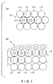
  • Fig. 1 shows spherical semiconductors 11a, 11b, 11c, 11d arranged in a hexagonal lattice, which is an example (example 1) of a three-dimensional arrangement of spherical semiconductors in a cluster spherical semiconductor device 12 according to the present invention.
  • Fig. 1(A) is a top view thereof.
  • Fig. 1(A) illustrates an arrangement of the spherical semiconductors 11a, 11b, 11c, 11d in each layer of the cluster spherical semiconductor device 12 which is composed of a layered body.
  • the spherical semiconductors 11a, 11b, 11c, 11d in the respective layers are arranged in a hexagonal lattice. Namely, one spherical semiconductor 11a, 11b is surrounded in contact with six spherical semiconductors 11a, 11b ⁇ in a layer.
  • the packing efficiency thereof is about 60%.
  • the respective spherical semiconductor devices 11a, 11b ⁇ in this arrangement have 8 positions where a spherical bump 13 is to be disposed, 6 positions of these portions being in a layer and 2 positions being up and down. That is, each spherical semiconductor 11a, 11b ⁇ has the spherical bump 13 at a portion in contact with the adjacent semiconductors 11a, 11b ⁇ .
  • the cluster spherical semiconductor device 12 according to the present invention has advantages in the utility efficiency of a space and the number of electrical connections, in relation to the conventional cluster spherical semiconductor device 42.

Landscapes

  • Wire Bonding (AREA)
  • Semiconductor Integrated Circuits (AREA)
  • Photovoltaic Devices (AREA)

Abstract

A cluster spherical semiconductor device includes a plurality of spherical semiconductors cluster-connected to each other. In the cluster spherical semiconductor device, the spherical semiconductors are arranged in a hexagonal lattice, a dense hexagonal lattice and a body-centered cubic lattice. <IMAGE>

Description

Field of the Invention
The present invention relates to a cluster spherical semiconductor device having a plurality of spherical semiconductors cluster-connected to each other.
Related Art
A three-dimensional arrangement of a spherical semiconductor in a conventionally proposed cluster spherical semiconductor device is a simple tetragonal cubic lattice. Fig. 4(A) shows a perspective view of this arrangement. A cluster spherical semiconductor device 42 requires an electrode for electrically connecting a plurality of spherical semiconductors 41a, 41b to each other, or for connecting the spherical semiconductors 41a, 41b to another semiconductor device or a substrate. As disclosed in Japanese Patent Application No. 031189/2000, an electrode is provided in the conventionally proposed spherical semiconductors 41, 41b ··· by disposing a spherical bump 43. The disposition thereof is shown in Fig. 4(B).
The cluster spherical semiconductor device arranged in the simple tetragonal cubic lattice arrangement as shown in Fig. 4(A) has a disadvantage about utility efficiency of a space, with a packing efficiency thereof being at most 53%. This arrangement is also unfavorable with respect to the number of electrical connections, because the number of locations where the spherical bump 43 is to be disposed is at most 6, as shown in Fig. 4(B), which is limited to front, back, right, left, up and down of the spherical semiconductors 41a, 41b, ···.
Disclosure of the Invention
The present invention is made to solve the above disadvantages. An object thereof is to provide a cluster spherical semiconductor device in which the utility efficiency of a space in a three-dimensional arrangement of a spherical semiconductor is increased, as well as the number of electrical connections between adjacent spherical semiconductors is increased.
The above subjects are solved by the invention described hereinbelow.
A cluster spherical semiconductor device according to the present invention includes a plurality of spherical semiconductors which are cluster-connected to each other, wherein the spherical semiconductors are arranged in a hexagonal lattice.
In the cluster spherical semiconductor device, since the spherical semiconductors are arranged in a hexagonal lattice, the utility efficiency of a space in a three-dimensional arrangement of the spherical semiconductors is increased, as well as the number of electrical connections between adjacent spherical semiconductors is increased.
The cluster spherical semiconductor device according to the present invention includes a plurality of spherical semiconductors which are cluster-connected to each other, wherein the spherical semiconductors are arranged in a dense hexagonal lattice.
In the cluster spherical semiconductor device, since the spherical semiconductors are arranged in a dense hexagonal lattice, the utility efficiency of a space in a three-dimensional arrangement of the spherical semiconductors is increased, as well as the number of electrical connections between adjacent spherical semiconductors is increased.
The cluster spherical semiconductor device according to the present invention includes a plurality of spherical semiconductors which are cluster-connected to each other, wherein the spherical semiconductors are arranged in a body-centered cubic lattice.
In the cluster spherical semiconductor device, since the spherical semiconductors are arranged in a body-centered cubic lattice, the utility efficiency of a space in a three-dimensional arrangement of the spherical semiconductors is increased, as well as the number of electrical connections between adjacent spherical semiconductors is increased.
Brief Description of the Drawings
  • Fig. 1 shows a hexagonal lattice arrangement of a spherical semiconductor in a cluster spherical semiconductor according to the present invention;
  • Fig. 2 shows a close packed hexagonal lattice arrangement of a spherical semiconductor in a cluster spherical semiconductor according to the present invention;
  • Fig. 3 shows a body-centered cubic lattice arrangement of a spherical semiconductor in a cluster spherical semiconductor according to the present invention; and
  • Fig. 4 shows a three-dimensional arrangement of a spherical semiconductor in a conventional cluster spherical semiconductor.
  • Detailed Description of the Invention
    Embodiments of the present invention are described hereinbelow. A spherical semiconductor is a semiconductor (semiconductor device) having an integrated circuit provided on the surface of a global body with dimension of about, for example, 1mm. A cluster-connection is to connect a plurality of semiconductors (semiconductor devices) electrically to each other, with a view to achieving an upgraded and improved performance, which can not be obtained by a single semiconductor. A cluster spherical semiconductor device includes a plurality of spherical semiconductors which are cluster-connected to each other. For example, a computer system, which is realized by cluster-connecting a plurality of spherical semiconductors having such functions as RAM (random access memory), ROM (read only memory), CPU (central processor unit), interface, etc., is composed of a cluster spherical semiconductor device.
    Fig. 1 shows spherical semiconductors 11a, 11b, 11c, 11d arranged in a hexagonal lattice, which is an example (example 1) of a three-dimensional arrangement of spherical semiconductors in a cluster spherical semiconductor device 12 according to the present invention. Fig. 1(A) is a top view thereof. Fig. 1(A) illustrates an arrangement of the spherical semiconductors 11a, 11b, 11c, 11d in each layer of the cluster spherical semiconductor device 12 which is composed of a layered body. As shown in Fig. 1(A), the spherical semiconductors 11a, 11b, 11c, 11d in the respective layers are arranged in a hexagonal lattice. Namely, one spherical semiconductor 11a, 11b is surrounded in contact with six spherical semiconductors 11a, 11b ··· in a layer.
    Fig. 1(B) is a perspective view of the cluster semiconductor device 12. As shown in Fig. 1(B), the layers of the cluster semiconductor device 12 are so laminated that phases of the spherical semiconductors 11a, 11b ··· in the respective layers are correspondent to each other. That is, the layers are piled up so as to bring the spherical semiconductors 11a, 11b ··· in a layer disposed directly above the spherical semiconductors 11a, 11b ··· in the lower layer.
    In the cluster spherical semiconductor device 12 which has the spherical semiconductors 11a, 11b ··· arranged in a hexagonal lattice as shown in Fig. 1, the packing efficiency thereof is about 60%. The respective spherical semiconductor devices 11a, 11b ··· in this arrangement have 8 positions where a spherical bump 13 is to be disposed, 6 positions of these portions being in a layer and 2 positions being up and down. That is, each spherical semiconductor 11a, 11b ··· has the spherical bump 13 at a portion in contact with the adjacent semiconductors 11a, 11b ···. As stated above, the cluster spherical semiconductor device 12 according to the present invention has advantages in the utility efficiency of a space and the number of electrical connections, in relation to the conventional cluster spherical semiconductor device 42.
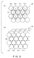
    Fig. 2 shows spherical semiconductors 21a, 21b, 21c, 21d arranged in a close packed hexagonal lattice, which is an example (example 2) of a three-dimensional arrangement of spherical semiconductors in a cluster spherical semiconductor device 22 according to the present invention. Fig. 2(A) is a top view thereof. Fig. 2(A) illustrates an arrangement of the spherical semiconductors 21a, 21b ··· in each layer of the cluster spherical semiconductor device 22 of a layered body. As shown in Fig. 2(A), the spherical semiconductors 21a, 21b ··· in the respective layers are arranged in a close packed hexagonal lattice. Namely, one spherical semiconductor 21a, 21b is surrounded in contact with six spherical semiconductors 21a, 21b ··· in a layer.
    Fig. 2(B) is a perspective view of the cluster semiconductor device 22. As shown in Fig. 2(B), the layers are so laminated that phases of the spherical semiconductors 21a, 21b ··· are staggered by 180 degrees. That is, the spherical semiconductors 21a, 21b ··· are piled up such that the spherical semiconductors 21a, 21b ··· of the upper layer are received in the recesses in the lower layer. Namely, the layers are laid up like a pyramid of oranges which heaped up in a fruit store.
    In the cluster spherical semiconductor device 22 which has the spherical semiconductors 21a, 21b ··· arranged in a close packed hexagonal lattice as shown in Fig. 2, the packing efficiency thereof is about 74%. The respective spherical semiconductors 21a, 21b ··· in this arrangement have 12 positions where a spherical bump 23 is to be, 6 positions of these portions being in a layer and 3 positions being in the upper and lower layers respectively. As described above, the cluster spherical semiconductor device 22 according to the present invention has advantages in the utility efficiency of a space and the number of electrical connections, in relation to the conventional cluster spherical semiconductor device 42.
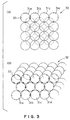
    Fig. 3 shows a spherical semiconductors 31a, 31b, 31c, 31d arranged in a body-centered cubic lattice, which is an example (example 3) of a three-dimensional arrangement of spherical semiconductors in a cluster spherical semiconductor device 32 according to the present invention. Fig. 3(A) is a top view thereof. Fig. 3(A) illustrates an arrangement of the spherical semiconductors 31a, 31b ··· in each layer of the cluster spherical semiconductor device 32 of a layered body. As shown in Fig. 3(A), the spherical semiconductors 31a, 31b ··· in the respective layers are arranged in a tetragonal lattice. Namely, one spherical semiconductor is surrounded in contact with four spherical semiconductors 31a, 31b ··· in a layer.
    Fig. 3(B) is a perspective view of the cluster semiconductor device 32. As shown in Fig. 3(B), the layers are so laminated that phases of the spherical semiconductors 31a, 31b are staggered by 180 degrees. That is, the spherical semiconductors are piled up such that the spherical semiconductors of the upper layer are received in the recesses in the lower layer.
    In the cluster spherical semiconductor device 32 which has the spherical semiconductors 31a, 31b ··· arranged in a body-centered cubic lattice as shown in Fig. 3, the packing efficiency thereof is about 61%. The respective spherical semiconductors 31a, 31b ··· in this arrangement have 12 positions where a spherical bump 33 is to be disposed, 4 positions of these portions being in a layer and 4 positions being in the upper and lower layers respectively. As described above, the cluster spherical semiconductor device 32 according to the present invention has advantages in the utility efficiency of a space and the number of electrical connections, in relation to the conventional cluster spherical semiconductor device 42.
    While the embodiments of the present invention has been described as above, the total number of the spherical semiconductors 11a, 11b, 21a, 21b, 31a, 31b ···, which are the constituents of the cluster spherical semiconductor devices 12, 22, 32, is not specifically referred, nor the total number of the layers. It is apparent that the cluster spherical semiconductor devices 12, 22, 32 having structural features of the present invention have a certain effect, although the cluster spherical semiconductor devices 12, 22, 32 compose parts of a whole semiconductor device. The present invention is not limited to the total number of spherical semiconductors or layers.
    As described above, in the cluster spherical semiconductor device according to the present invention, since the spherical semiconductors are arranged in a hexagonal lattice, the utility efficiency of a space in a three-dimensional arrangement of spherical semiconductors is increased, as well as the number of electrical connections between adjacent spherical semiconductors is increased.
    In the cluster spherical semiconductor device according to the present invention, since the spherical semiconductors are arranged in a close packed hexagonal lattice, the utility efficiency of a space in a three-dimensional arrangement of spherical semiconductors is increased, as well as the number of electrical connections between adjacent spherical semiconductors is increased.
    In the cluster spherical semiconductor device according to the present invention, since the spherical semiconductors are arranged in a body-centered cubic lattice, the utility efficiency of a space in a three-dimensional arrangement of spherical semiconductors is increased, as well as the number of electrical connections between adjacent spherical semiconductors is increased.

    Claims (4)

    1. A cluster spherical semiconductor device comprising a plurality of spherical semiconductors which are cluster-connected to each other,
         wherein said spherical semiconductors are arranged in a hexagonal lattice.
    2. A cluster spherical semiconductor device comprising a plurality of spherical semiconductors which are cluster-connected to each other,
         wherein said spherical semiconductors are arranged in a close packed hexagonal lattice.
    3. A cluster spherical semiconductor device comprising a plurality of spherical semiconductors which are cluster-connected to each other,
         wherein said spherical semiconductors are arranged in a body-centered cubic lattice.
    4. The cluster spherical semiconductor device as claimed in any one of claims 1 to 3,
         wherein each spherical semiconductor has a spherical bump at a portion being in contact with a spherical semiconductor adjacent thereto.
    EP01958486A 2000-08-28 2001-08-24 SPHERICAL SEMICONDUCTOR DEVICE CONNECTED IN A CLUSTER Withdrawn EP1251560A4 (en)

    Applications Claiming Priority (3)

    Application Number Priority Date Filing Date Title
    JP2000256564 2000-08-28
    JP2000256564A JP2002076249A (en) 2000-08-28 2000-08-28 Cluster spherical semiconductor
    PCT/JP2001/007281 WO2002019428A1 (en) 2000-08-28 2001-08-24 Cluster globular semiconductor device

    Publications (2)

    Publication Number Publication Date
    EP1251560A1 true EP1251560A1 (en) 2002-10-23
    EP1251560A4 EP1251560A4 (en) 2004-04-21

    Family

    ID=18745155

    Family Applications (1)

    Application Number Title Priority Date Filing Date
    EP01958486A Withdrawn EP1251560A4 (en) 2000-08-28 2001-08-24 SPHERICAL SEMICONDUCTOR DEVICE CONNECTED IN A CLUSTER

    Country Status (5)

    Country Link
    US (1) US20020153541A1 (en)
    EP (1) EP1251560A4 (en)
    JP (1) JP2002076249A (en)
    KR (1) KR20020044576A (en)
    WO (1) WO2002019428A1 (en)

    Family Cites Families (11)

    * Cited by examiner, † Cited by third party
    Publication number Priority date Publication date Assignee Title
    US5955776A (en) * 1996-12-04 1999-09-21 Ball Semiconductor, Inc. Spherical shaped semiconductor integrated circuit
    JP3955394B2 (en) * 1998-07-09 2007-08-08 新日鉄マテリアルズ株式会社 Manufacturing method of spherical semiconductor device
    JP2000031189A (en) * 1998-07-09 2000-01-28 Nippon Steel Corp Spherical semiconductor device
    JP2000031461A (en) * 1998-07-09 2000-01-28 Asahi Optical Co Ltd Semiconductor device and semiconductor assembly equipment
    JP3056467B2 (en) * 1998-09-08 2000-06-26 有限会社デジタル・ウェーブ Semiconductor device manufacturing substrate, method of manufacturing the same, photoelectric conversion device, and method of manufacturing the same
    WO2000030534A1 (en) * 1998-11-25 2000-06-02 Ball Semiconductor, Inc. Spherically-shaped biomedical ic
    JP2000216329A (en) * 1999-01-25 2000-08-04 Seiko Epson Corp Spherical semiconductor and semiconductor device using the same
    JP2000216334A (en) * 1999-01-25 2000-08-04 Seiko Epson Corp Semiconductor device
    WO2000058872A1 (en) * 1999-03-26 2000-10-05 Ball Semiconductor, Inc. Field programmable ball array
    JP2001102618A (en) * 1999-09-30 2001-04-13 Sony Corp Light receiving device
    JP3580749B2 (en) * 2000-02-18 2004-10-27 シャープ株式会社 Mounting method of granular semiconductor device

    Also Published As

    Publication number Publication date
    WO2002019428A1 (en) 2002-03-07
    JP2002076249A (en) 2002-03-15
    KR20020044576A (en) 2002-06-15
    EP1251560A4 (en) 2004-04-21
    US20020153541A1 (en) 2002-10-24

    Similar Documents

    Publication Publication Date Title
    US6927478B2 (en) Reduced size semiconductor package with stacked dies
    US9818625B2 (en) Stacked semiconductor die assemblies with thermal spacers and associated systems and methods
    US6559526B2 (en) Multiple-step inner lead of leadframe
    CN1052114C (en) Method for producing single chip electronic device by way of piling IC chip plane array
    US7026709B2 (en) Stacked chip-packaging structure
    JP2505958B2 (en) Integrated circuit device packaging method
    US5838545A (en) High performance, low cost multi-chip modle package
    US5737192A (en) Density improvement in integration modules
    US20100224977A1 (en) Semiconductor device and method for fabricating the same
    US20170125378A1 (en) Semiconductor package including stepwise stacked chips
    CA2333973A1 (en) Scaleable integrated data processing device
    KR20160138255A (en) Stacked semiconductor die assemblies with partitioned logic and associated systems and methods
    TWI695486B (en) Multi-stacked semiconductor device assembly containing different semiconductor die and manufacturing method thereof
    JP2002204053A (en) Circuit mounting method, circuit mounting substrate, and semiconductor device
    US20050023674A1 (en) Multi-chip module having bonding wires and method of fabricating the same
    JP7210066B2 (en) Semiconductor module, manufacturing method thereof, and semiconductor module mounted body
    US20020180020A1 (en) Three-dimension multi-chip stack package technology
    JP3832170B2 (en) Multi-bare chip assembly
    US6661086B2 (en) Three-dimensionally embodied circuit with electrically connected semiconductor chips
    US6060761A (en) Lateral type transistor
    US6858930B2 (en) Multi chip module
    US20020153541A1 (en) Cluster globular semiconductor device
    JP2737322B2 (en) Memory module
    US20030094628A1 (en) Memory module structure
    JPH023621Y2 (en)

    Legal Events

    Date Code Title Description
    PUAI Public reference made under article 153(3) epc to a published international application that has entered the european phase

    Free format text: ORIGINAL CODE: 0009012

    17P Request for examination filed

    Effective date: 20020524

    AK Designated contracting states

    Kind code of ref document: A1

    Designated state(s): AT BE CH CY DE DK ES FI FR GB GR IE IT LI LU MC NL PT SE TR

    A4 Supplementary search report drawn up and despatched

    Effective date: 20040305

    RIC1 Information provided on ipc code assigned before grant

    Ipc: 7H 01L 25/04 A

    Ipc: 7H 01L 25/065 B

    RBV Designated contracting states (corrected)

    Designated state(s): AT BE CH CY DE FR GB LI NL

    STAA Information on the status of an ep patent application or granted ep patent

    Free format text: STATUS: THE APPLICATION IS DEEMED TO BE WITHDRAWN

    18D Application deemed to be withdrawn

    Effective date: 20060726