EP1251555A2 - Method of fabricating HBT devices - Google Patents
Method of fabricating HBT devices Download PDFInfo
- Publication number
- EP1251555A2 EP1251555A2 EP02008252A EP02008252A EP1251555A2 EP 1251555 A2 EP1251555 A2 EP 1251555A2 EP 02008252 A EP02008252 A EP 02008252A EP 02008252 A EP02008252 A EP 02008252A EP 1251555 A2 EP1251555 A2 EP 1251555A2
- Authority
- EP
- European Patent Office
- Prior art keywords
- layer
- base
- photoresist
- emitter
- ohmic metal
- Prior art date
- Legal status (The legal status is an assumption and is not a legal conclusion. Google has not performed a legal analysis and makes no representation as to the accuracy of the status listed.)
- Granted
Links
Images




Classifications
-
- H—ELECTRICITY
- H10—SEMICONDUCTOR DEVICES; ELECTRIC SOLID-STATE DEVICES NOT OTHERWISE PROVIDED FOR
- H10D—INORGANIC ELECTRIC SEMICONDUCTOR DEVICES
- H10D8/00—Diodes
- H10D8/01—Manufacture or treatment
- H10D8/051—Manufacture or treatment of Schottky diodes
-
- H—ELECTRICITY
- H10—SEMICONDUCTOR DEVICES; ELECTRIC SOLID-STATE DEVICES NOT OTHERWISE PROVIDED FOR
- H10D—INORGANIC ELECTRIC SEMICONDUCTOR DEVICES
- H10D10/00—Bipolar junction transistors [BJT]
- H10D10/01—Manufacture or treatment
- H10D10/021—Manufacture or treatment of heterojunction BJTs [HBT]
-
- H—ELECTRICITY
- H10—SEMICONDUCTOR DEVICES; ELECTRIC SOLID-STATE DEVICES NOT OTHERWISE PROVIDED FOR
- H10D—INORGANIC ELECTRIC SEMICONDUCTOR DEVICES
- H10D10/00—Bipolar junction transistors [BJT]
- H10D10/80—Heterojunction BJTs
- H10D10/821—Vertical heterojunction BJTs
-
- H—ELECTRICITY
- H10—SEMICONDUCTOR DEVICES; ELECTRIC SOLID-STATE DEVICES NOT OTHERWISE PROVIDED FOR
- H10D—INORGANIC ELECTRIC SEMICONDUCTOR DEVICES
- H10D8/00—Diodes
- H10D8/60—Schottky-barrier diodes
-
- H—ELECTRICITY
- H10—SEMICONDUCTOR DEVICES; ELECTRIC SOLID-STATE DEVICES NOT OTHERWISE PROVIDED FOR
- H10D—INORGANIC ELECTRIC SEMICONDUCTOR DEVICES
- H10D84/00—Integrated devices formed in or on semiconductor substrates that comprise only semiconducting layers, e.g. on Si wafers or on GaAs-on-Si wafers
- H10D84/60—Integrated devices formed in or on semiconductor substrates that comprise only semiconducting layers, e.g. on Si wafers or on GaAs-on-Si wafers characterised by the integration of at least one component covered by groups H10D10/00 or H10D18/00, e.g. integration of BJTs
- H10D84/611—Combinations of BJTs and one or more of diodes, resistors or capacitors
- H10D84/613—Combinations of vertical BJTs and one or more of diodes, resistors or capacitors
- H10D84/617—Combinations of vertical BJTs and only diodes
-
- H—ELECTRICITY
- H10—SEMICONDUCTOR DEVICES; ELECTRIC SOLID-STATE DEVICES NOT OTHERWISE PROVIDED FOR
- H10D—INORGANIC ELECTRIC SEMICONDUCTOR DEVICES
- H10D62/00—Semiconductor bodies, or regions thereof, of devices having potential barriers
- H10D62/80—Semiconductor bodies, or regions thereof, of devices having potential barriers characterised by the materials
- H10D62/85—Semiconductor bodies, or regions thereof, of devices having potential barriers characterised by the materials being Group III-V materials, e.g. GaAs
Definitions
- the present invention relates to a method for fabricating integrated circuits, and more particularly, to a method of fabricating heterojunction bipolar transistors (HBTs) having extremely high speed at very low currents.
- HBTs heterojunction bipolar transistors
- the present invention provides a method for forming very high speed HBTs with low power consumption by providing an arrangement for achieving extremely small emitter area and extremely small base area, with a large portion of both the emitter area and the base area being contacted with metal.
- the collector metal contact can be closely spaced to the emitter to achieve a low parasitic collector resistance.
- a collector layer, a base layer and an emitter layer are formed in a stacked arrangement on a substrate.
- a layer of material is then deposited on the emitter layer, a first photoresist is formed over a portion of the material, and the layer of material and the emitter layer are etched using the first photoresist as a mask to form an emitter mesa on the base layer. At this point, the material remains on top of the emitter mesa and the first photoresist remains on top of the material.
- a second photoresist is deposited on the base layer. The second photoresist is patterned and developed on the base layer to expose a portion of the base layer surrounding the emitter mesa. A base ohmic metal is then formed on the first and second photoresists and the exposed portion of the base layer.
- the first and second photoresists, with the base ohmic material thereon, are lifted off, leaving the base ohmic material on the base layer.
- the base ohmic material is uniformly spaced relative to the emitter mesa.
- the emitter mesa and a portion of the base ohmic metal is covered with a third photoresist.
- the base layer is then etched to undercut the base ohmic metal, thereby reducing the size of the base layer and, correspondingly, significantly reducing the base-collector parasitic capacitance.
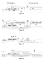
- Figs. 1 to 21 are sectional views of successive steps for simultaneously forming an HBT and a Schottky diode in accordance with the present invention.
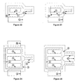
- Figs. 22 to 25 are plan views showing mask layer arrangements for layout of the HBT device with an advantageous base ohmic design.
- the primary factor which controls the speed of an HBT transistor is the growth of the emitter, base, and collector layers of the device. However, once the layers have been grown, it is the method of etching the emitter, base, and collector and the method of making metal contacts to those layers that determine the device's operating speed as a function of current. From his studies, the inventor has determined that key attributes that are needed in fabricating a HBT transistor of a given layer growth to achieve high frequency operation at the lowest possible current include:
- collector metal contact closely spaced to the emitter for a low parasitic collector resistance.
- the present invention provides a process that can built an HBT device with the above attributes to permit the fabrication of complex HBT integrated circuits that operate at very high speeds and low currents.
- This invention consists of a method of fabricating a HBT transistor with a small emitter area, a small base area, most of the emitter area contacted with metal, most of the base area outside of the emitter contacted with metal, and a collector ohmic metal placed close to the device emitter and base ohmic metal.
- the invention also includes a method of partially undercutting the base ohmic metal along all external edges of the metal to further reduce the device's parasitic base - collector capacitance, and covering the undercut base ohmic metal with a sloped edge polymer to provide metal step coverage.
- a Schottky diode can be fabricated within the process steps required to form the HBT transistor; therefore, no additional process steps are needed to build the Schottky diode.
- the concepts of this invention can be applied to GaAs, InP, and most, if not all, HBT semiconductor materials.
- the layers of a HBT device 10 including a heavily doped sub-collector 12, a lightly doped collector 14, a heavily doped base 16, and a lightly doped emitter 18, each layer of which may be comprised of several sublayers, are grown by one of several conventional techniques, such as MBE or MOCVD on a substrate 20.
- the SiN (or SiO 2 ) layer 22 is etched to within about 100 ⁇ to 400 ⁇ of the emitter surface using an anisotropic dry etch, then the etch is completed to the emitter surface with an isotropic etch, such as a wet etch in BOE (buffered oxide etch), that etches about 500 ⁇ to 800 ⁇ of SiN (or SiO 2 ) layer 22 that undercuts the photoresist 24 by this amount, as shown in Figure 2.
- an isotropic etch such as a wet etch in BOE (buffered oxide etch
- the semiconductor material forming the emitter layer 18 is etched using an isotropic or a partially anisotropic dry etch, or a wet etch, or a combination of the two to the appropriate depth for making contact to the base layer 16, as shown in Figure 3.
- the SiN (or SiO 2 ) layer 22 is etched laterally by 500 ⁇ to 800 ⁇ with a wet BOE etch, as shown in Figure 4 to reduce the SiN (or SiO 2 ) layer 22 which extends beyond the emitter layer 18. (For final emitter widths of ⁇ .3 ⁇ m it may be desirable to delete this step).
- a base ohmic resist layer 28 is coated on the wafer and patterned with a re-entrant profile for metal lift off using any of several conventional processes, such as NH 3 image reversal on a positive resist, a chlorobenzene treated positive resist, or a negative i-line resist, as diagramed in Figure 5.
- a base ohmic metal 30 is then deposited onto the wafer covering the lift-off resist 28, the resist 24 over the emitter 18, and the base surface area next to the emitter at a thickness somewhat less or equal to the height of the emitter region, as shown in Figure 6.
- the emitter resist 24 and the base ohmic resist 28 is lifted off leaving only the base ohmic metal 30 and the SiN (or SiO 2 ) layer 22 above the emitter region 18, as shown in Figure 7.
- a base mesa photoresist pattern 32 is used to cover the emitter region 18 of the device, then the base region 16 is etched by a wet etch, an isotropic dry etch, or a partially anisotropic dry etch to a depth somewhat past the base region, typically to a depth of 500 ⁇ to 3000 ⁇ . If a Schottky diode is also being fabricated, the depth of this etch can be to the surface of the Schottky diode surface. Although an anisotropic dry etch can be used for this etch, an isotropic or mostly isotropic etch is preferably used to undercut the base ohmic metal 30, reducing the base - collector parasitic capacitance. If a dry etch is used to etch the base layer 16, it can be followed by a brief wet etch to eliminate surface damage.
- the HBT device 10 and Schottky diode 26 cross-section after this process step is shown in Figure 8.
- a collector ohmic resist 34 is patterned to make contact to the sub-collector 12 of both the HBT device 10 and the Schottky diode 26, as shown in device cross sections in Figure 9.
- the collector region 14 is etched with an isotropic wet etch, an isotropic dry etch or a partially isotropic dry etch to the depth of the sub-collector surface 12, then a collector ohmic metal 36 is deposited into the etched region at a thickness about equal to the depth of the etch or slightly greater, as shown in Figure 10.
- the resist 34 and the collector ohmic metal 36 over it are lifted off using any conventional resist lift-off procedure, as diagramed in Figure 11.
- the collector ohmic metal 36 and the base ohmic metal 30 are alloyed using a short furnace anneal or a rapid thermal anneal (RTA) at about 350 C to 400°C.
- RTA rapid thermal anneal
- the wafer is covered with a polymer 38 at a thickness of about 500 ⁇ to 1000 ⁇ thicker than the distance from the top of the SiN (or SiO 2 ) layer 22 to the bottom of the etched base mesa region (or the surface of the Schottky diode).
- the polymer 38 is a planarizing material, such as benzocylobutene (BCB)
- the polymer is cured and flowed flat (as shown in Figure 12).
- the polymer directly covering the emitter mesa 18 and the collector layer 14 is a non-planarizing polymer 40, such as polyimide, it is first cured, then a second planarizing layer 42 is coated over the non-planarizing polymer 40.
- the planarizing layer 42 is cured to flow flat over the non-planarizing polymer 40.
- a diagram showing the device cross sections with the single planarizing polymer layer 38 is shown in Figure 12.
- a diagram showing similar cross sections for the combination of a non-planarizing polymer 40 covered with a planarizing layer 42 is shown in Figure 13.
- planarized polymer 38 of Figure 12 or the polymer 40 plus the planarizing layer 42 of Figure 13 is etched with a dry etch using a gas such as O 2 or SF 6 , CF 4 , CHF 3 , or NF 3 with O 2 until the surface of the SiN (or SiO 2 ) layer 22 over the emitter 18 is exposed with about 100 ⁇ to 500 ⁇ of the SiN (or SiO 2 ) layer 22 protruding above the polymer 38, as indicated in the device cross sections in Figure 14. If the two layer arrangement of Figure 13 is used, the SiN (or SiO 2 ) layer 22 will protrude above the polymer 40 which has been planarized during the etch of the planarizing layer 42. For purposes of simplification, the following discussion will assume a single layer of planarizing polymer 38 is being used.
- a photoresist layer 44 is coated over the polymer layer 38 and patterned to cover the HBT 10 and Schottky device 26, except for regions to make contact to the collector ohmic metal 36 of the HBT device and the cathode of the Schottky diode, and for a hole in the polymer 38 to make contact to the base ohmic metal 30 and the anode of the Schottky device.
- This step is shown in Figure 15, except this cross section does not show the contact to the base ohmic metal 30 for purposes of drawing simplification.
- the polymer 38 is etched, using the photoresist 44, with a dry etch using SF 6 , CHF 3 , CHF 4 , NF 3 or equivalent gas with O 2 gas ratios set so that about a 2:1 to 5:1 partially anisotropic etch is achieved.
- a brief wet etch that removes about 50 ⁇ to 300 ⁇ of material from the Schottky diode anode (and other areas not protected by the polymer 38 and resist 44) can be used to eliminate surface damage from the dry etch prior to stripping the photoresist 44 by conventional means.
- the device cross sections after this process step are shown in the sketches in Figure 16.
- the SiN (or SiO 2 ) layer 22 over the emitter 18 is removed with a wet etch in buffered oxide etch.
- the wafer is coated with a photoresist 46, then a lift-off resist pattern is formed over the emitter 18 of the HBT device 10 and the anode of the Schottky diode 26 using any of several conventional means such as i-line negative resist, a NH 3 image reversal of a positive resist, or a chlorobenzene treated positive resist.
- a metal 48 which makes a good ohmic contact to the emitter of the HBT device 10 and a Schottky barrier contact to the lightly doped collector region of the Schottky diode 26, is evaporated onto the wafer, as illustrated in Figure 17.
- the resist 46 and the metal 48 on top of it are lifted off by any conventional lift-off process.
- a new photoresist layer 50 is then coated and patterned over the HBT transistor 10 and Schottky diode 26 for the purpose of forming isolating regions for the devices.
- the HBT 10 and Schottky diode 26 can be isolated by using an implanted species, such as H, B, or O, to create implant damage areas 52 in the remaining lightly doped collector region 14 and the more heavily doped subcollector 12 using multiple doses and energies of implanted species as necessary to create uniform damage throughout these regions, as indicated in device cross sections shown in Figure 18.
- a wet etch or a slightly isotropic dry etch can be used to etch through the collector 14 and sub-collector region 12 to the substrate region 20, as shown in device cross sections in Figure 19, to create isolating trenches 54.
- the isolation resist 50 is subsequently stripped using standard techniques. Then the wafer processing is completed by conventional process procedures, such as:'
- Additional layers of dielectrics, vias in the dielectrics, and patterned metal films can be added to complete the- fabrication of integrated circuits in accordance with conventional techniques.
- the SiN (or SiO 2 ) layer 22 deposited in Figure 2 can be replaced with a metallic film, such as the emitter metal 60 shown in Figure 21.
- This metal 60 can be Ti, TiN, W, TiW or similar metal.
- the metal 60 is patterned in a manner similar to that described previously with regard to the SiN (or SiO 2 ) film 22. For example, an anisotropic dry etch can be used to etch most of the thickness of the metal layer 60, then the etch is completed with an isotropic etch that is selective to the emitter semiconductor layer. The process is continued with the steps shown in Figures 3 and 5 through 16, discussed previously.
- the steps shown in Figure 17 are not required for making metal contact to the emitter.
- the metal deposition step shown in Figure 17 can still be used to form the Schottky contact for the Schottky diode 26 if one is being fabricated at the same time as the HBT 10.
- this metal deposition can be deleted from the process flow, and the first interconnect metal 58 shown in Figure 20 can be used to form the anode of the Schottky diode 26, provided the bottom layer of the first interconnect metal can be used to form the anode of the Schottky diode 26.
- the bottom layer of the first interconnect metal 58 is chosen to form a Schottky barrier contact to the lightly doped collector region.
- the arrangement of the final HBT 10 and Schottky diode 26 cross sections for this alternative process are shown in Figure 21. Although the Schottky diode 26 has been described as being adjacent HBT 10, it may also be elsewhere on the same substrate.
- the process flows described above have a particular advantage when the base ohmic metal region 30 is designed to form a narrow ring around the emitter 18 and the area on the base ohmic metal 30 that is to be contacted by external metal has a narrow width.
- a sketch diagramming the first five mask layers for the layout of a HBT device 10 with the advantageous base ohmic design is shown in Figure 22.
- the emitter layer "A" mask size can have a width of about .3 ⁇ m to 3 ⁇ m or larger with a length of about .5 ⁇ m to 20 ⁇ m or larger.
- the final emitter size will be somewhat smaller due to the isotropic or partial isotropic etches used in etching the emitter 18.
- the base ohmic metal layer “B” extends only about .3 ⁇ m to .5 ⁇ m past the emitter layer "A,” and the area of the base ohmic metal 30 that is to be contacted with external metal is defined at a width of only about .4 ⁇ m to 1.0 ⁇ m.
- the base ohmic metal 30 can be undercut by about .1 ⁇ m to .2 ⁇ m during the etching of the base semiconductor region 16. This reduces the collector-base parasitic device capacitance with little or no increase of the parasitic base resistance.
- the collector ohmic region “D” can be placed very close to the base ohmic region within about .3 ⁇ m to .5 ⁇ m.
- the planarized polymer layer "E" only has to extend about .3 ⁇ m past the base ohmic metal 30 to provide for the self-aligned emitter metal region (not shown) with a sloped edge, which provides for metal step coverage over the undercut base ohmic metal 30. Also, a contact hole is provided in the polymer 38 for the base ohmic metal 30. It should be noted the polymer layer 38 can also be defined to extend past the collector ohmic metal "D” with a similar contact hole in the polymer 38 to the collector ohmic metal 36 to ensure the region between the collector ohmic metal 36 and etched semiconductor remains filled with polymer 38.
- FIG 23 An alternate layout of the HBT device 10 is shown in Figure 23.
- the base ohmic metal "B" extends only partially around the emitter region "A," further reducing the base - collector capacitance at the expense of some increase in the base parasitic resistance.
- the base ohmic metal 30 can be contacted with a single base ohmic region for minimum base-collector capacitance or with 2 or more base ohmic regions for lower base parasitic resistance.
- HBT devices can also be connected with 2 collector ohmic regions "D" as shown in Figure 24.
- Other conventional HBT device layouts can be used with the process flows described above.
Landscapes
- Bipolar Transistors (AREA)
- Bipolar Integrated Circuits (AREA)
- Electrodes Of Semiconductors (AREA)
Abstract
Description
In conjunction with this, the collector metal contact can be closely spaced to the emitter to achieve a low parasitic collector resistance. To achieve this in accordance with one embodiment of the invention, a collector layer, a base layer and an emitter layer are formed in a stacked arrangement on a substrate. A layer of material is then deposited on the emitter layer, a first photoresist is formed over a portion of the material, and the layer of material and the emitter layer are etched using the first photoresist as a mask to form an emitter mesa on the base layer. At this point, the material remains on top of the emitter mesa and the first photoresist remains on top of the material. Next, a second photoresist is deposited on the base layer. The second photoresist is patterned and developed on the base layer to expose a portion of the base layer surrounding the emitter mesa. A base ohmic metal is then formed on the first and second photoresists and the exposed portion of the base layer. The first and second photoresists, with the base ohmic material thereon, are lifted off, leaving the base ohmic material on the base layer. By virtue of the preceding steps, the base ohmic material is uniformly spaced relative to the emitter mesa. Next, the emitter mesa and a portion of the base ohmic metal is covered with a third photoresist. The base layer is then etched to undercut the base ohmic metal, thereby reducing the size of the base layer and, correspondingly, significantly reducing the base-collector parasitic capacitance.

Claims (9)
- A method of forming a heterojunction bipolar transistor (HBT) comprising:a) forming a collector layer, a base layer and an emitter layer in a stacked arrangement on a substrate;b) depositing a layer of material on said emitter layer and forming a first photoresist over a portion of said material, etching said layer of material and said emitter layer using said first photoresist as a mask to form an emitter mesa on the base layer with the layer of material on top of said emitter mesa and said first photoresist on top of said layer of material;c) depositing a second photoresist on said base layer;d) patterning and developing said second photoresist on said base layer to expose a portion of the base layer surrounding the emitter mesa;e) depositing a base ohmic metal on said first and second photoresists and the exposed portion of the base layer;f) lifting off the first and second photoresists and the base ohmic metal formed over it leaving the base ohmic metal on the base layer, wherein the base ohmic metal is uniformly spaced relative to the emitter mesa;g) covering the emitter mesa and a portion of the base ohmic metal with a third photoresist; andh) etching the base layer to undercut the base ohmic metal to reduce the size of the base layer.
- A method according to claim 1, further comprising removing the third photoresist and forming a polymer over the emitter mesa and the base layer, wherein the polymer extends on the base layer under the undercut area of the base ohmic metal.
- A method according to claim 1, further comprising:removing the third photoresist;forming a fourth photoresist over the emitter mesa and the base layer;patterning the fourth photoresist to expose a portion of the collector layer; anddepositing a collector ohmic metal on said exposed portion of the collector layer.
- A method according to claim 3, further comprising removing the fourth photoresist and forming a polymer over the emitter mesa and the base layer, wherein the polymer extends on the base layer under the undercut area of the base ohmic metal.
- A method according to claim 1, wherein the material formed on top of the emitter mesa is a sacrificial material, preferably a dielectric, and/or the method further comprises the steps of removing the sacrificial material; and depositing a layer of metal over the top of the emitter mesa to form an emitter ohmic contact.
- A method according to claim 1, wherein the material formed on top of the emitter mesa is a metal which forms an emitter ohmic contact for the HBT.
- A method of forming a device including an HBT and a Schottky diode simultaneously comprising:a) forming a collector layer, a base layer and an emitter layer in a stacked arrangement on a substrate;b) depositing a layer of material on said emitter layer and forming a first photoresist over a portion of said material, etching said layer of material and said emitter layer using said first photoresist as a mask to form an emitter mesa on the base layer with the layer of material on top of said emitter mesa and said first photoresist on top of said layer of material;c) depositing a second photoresist on said base layer;d) patterning and developing said second photoresist on said base layer to expose a portion of the base layer surrounding the emitter mesa;e) depositing a base ohmic metal on said first and second photoresists and the exposed portion of the base layer;f) lifting off the first and second photoresists and the base ohmic metal formed over it leaving the base ohmic metal on the base layer, wherein the base ohmic metal is uniformly spaced relative to the emitter mesa;g) covering the emitter mesa and a portion of the base ohmic metal with a third photoresist; andh) etching the base layer to undercut the base ohmic metal to reduce the size of the base layer;i) removing the third photoresist;j) forming a fourth photoresist over the emitter mesa and the exposed surface of the base layer;k) patterning the fourth photoresist to expose a portion of the collector layer;l) depositing a collector ohmic metal on the exposed surface of the collector layer;m) removing the fourth photoresist;n) depositing and etching a polymer layer so that polymer covers the emitter mesa, the base ohmic metal, a portion of the collector ohmic metal and a portion of the collector layer excluding at least part of the upper surface of the collector layer;o) removing the material covering the upper surface of the emitter mesa;p) depositing a fifth photoresist over the emitter mesa, the exposed surface of the collector layer and over the collector ohmic metal and patterning the fifth photoresist to expose an upper surface of the emitter mesa and a portion of the collector layer where the Schottky diode is to be formed; andq) depositing a metal layer over the exposed upper surface of the emitter mesa and over the exposed portion of the collector layer where the Schottky diode is to be formed, thereby forming an emitter ohmic metal and the anode of the Schottky diode.
- A method according to claim 7, further comprising:removing the fifth photoresist;depositing a sixth photoresist on both the HBT and the Schottky diode and patterning the sixth photoresist to expose a portion of the collector layer around the HBT and the Schottky diode; andforming an isolation region around the HBT and the Schottky diode.
- A method according to claim 8, wherein the isolation region is a trench, and/or
wherein the isolation region is an implant damage region, and/or
wherein the material is a dielectric material.
Applications Claiming Priority (2)
| Application Number | Priority Date | Filing Date | Title |
|---|---|---|---|
| US837966 | 2001-04-19 | ||
| US09/837,966 US6406965B1 (en) | 2001-04-19 | 2001-04-19 | Method of fabricating HBT devices |
Publications (3)
| Publication Number | Publication Date |
|---|---|
| EP1251555A2 true EP1251555A2 (en) | 2002-10-23 |
| EP1251555A3 EP1251555A3 (en) | 2004-06-16 |
| EP1251555B1 EP1251555B1 (en) | 2007-08-29 |
Family
ID=25275903
Family Applications (1)
| Application Number | Title | Priority Date | Filing Date |
|---|---|---|---|
| EP02008252A Expired - Lifetime EP1251555B1 (en) | 2001-04-19 | 2002-04-18 | Method of fabricating HBT devices |
Country Status (5)
| Country | Link |
|---|---|
| US (1) | US6406965B1 (en) |
| EP (1) | EP1251555B1 (en) |
| JP (1) | JP2002368006A (en) |
| DE (1) | DE60222046T2 (en) |
| TW (1) | TW536824B (en) |
Cited By (1)
| Publication number | Priority date | Publication date | Assignee | Title |
|---|---|---|---|---|
| WO2015120432A1 (en) * | 2014-02-10 | 2015-08-13 | United Silicon Carbide, Inc. | Trenched and implanted bipolar junction transistor |
Families Citing this family (14)
| Publication number | Priority date | Publication date | Assignee | Title |
|---|---|---|---|---|
| TW483171B (en) * | 2000-03-16 | 2002-04-11 | Trw Inc | Ultra high speed heterojunction bipolar transistor having a cantilevered base. |
| JP4895421B2 (en) * | 2000-12-04 | 2012-03-14 | ルネサスエレクトロニクス株式会社 | Method for manufacturing heterojunction bipolar transistor |
| US20030129843A1 (en) * | 2001-10-05 | 2003-07-10 | Yongming Cai | Planarizing recess etch |
| US6797995B2 (en) * | 2002-02-14 | 2004-09-28 | Rockwell Scientific Licensing, Llc | Heterojunction bipolar transistor with InGaAs contact and etch stop layer for InP sub-collector |
| JP2004296567A (en) * | 2003-03-26 | 2004-10-21 | Renesas Technology Corp | Semiconductor device and method of manufacturing the same |
| US6806129B1 (en) | 2003-05-09 | 2004-10-19 | Agilent Technologies, Inc. | Self-aligned process using indium gallium arsenide etching to form reentry feature in heterojunction bipolar transistors |
| US7071498B2 (en) * | 2003-12-17 | 2006-07-04 | Nitronex Corporation | Gallium nitride material devices including an electrode-defining layer and methods of forming the same |
| JP2009289861A (en) * | 2008-05-28 | 2009-12-10 | Sharp Corp | Semiconductor device, and mehod for manufacturing thereof |
| EP2180517A1 (en) * | 2008-10-24 | 2010-04-28 | Epcos Ag | Pnp bipolar transistor with lateral collector and method of production |
| US9847407B2 (en) * | 2011-11-16 | 2017-12-19 | Skyworks Solutions, Inc. | Devices and methods related to a gallium arsenide Schottky diode having low turn-on voltage |
| US9461153B2 (en) | 2011-11-16 | 2016-10-04 | Skyworks Solutions, Inc. | Devices and methods related to a barrier for metallization of a gallium based semiconductor |
| JP6605977B2 (en) * | 2016-02-10 | 2019-11-13 | アンリツ株式会社 | Semiconductor integrated circuit and manufacturing method of semiconductor integrated circuit |
| JP2019033180A (en) * | 2017-08-08 | 2019-02-28 | 株式会社村田製作所 | Semiconductor device |
| CN113066723B (en) * | 2021-03-19 | 2022-06-07 | 厦门市三安集成电路有限公司 | Heterojunction bipolar transistor and manufacturing method thereof |
Family Cites Families (7)
| Publication number | Priority date | Publication date | Assignee | Title |
|---|---|---|---|---|
| JPH01238161A (en) * | 1988-03-18 | 1989-09-22 | Fujitsu Ltd | Semiconductor device and manufacture thereof |
| US5160994A (en) * | 1990-02-19 | 1992-11-03 | Nec Corporation | Heterojunction bipolar transistor with improved base layer |
| US5268315A (en) * | 1992-09-04 | 1993-12-07 | Tektronix, Inc. | Implant-free heterojunction bioplar transistor integrated circuit process |
| US5486483A (en) | 1994-09-27 | 1996-01-23 | Trw Inc. | Method of forming closely spaced metal electrodes in a semiconductor device |
| EP0710984B1 (en) * | 1994-11-02 | 2001-08-08 | Trw Inc. | Method of fabricating monolithic multifunction integrated circuit devices |
| US5804487A (en) * | 1996-07-10 | 1998-09-08 | Trw Inc. | Method of fabricating high βHBT devices |
| US5946582A (en) * | 1997-01-07 | 1999-08-31 | Telcordia Technologies, Inc. | Method of making an InP-based heterojunction bipolar transistor with reduced base-collector capacitance |
-
2001
- 2001-04-19 US US09/837,966 patent/US6406965B1/en not_active Expired - Lifetime
-
2002
- 2002-04-03 TW TW091106732A patent/TW536824B/en not_active IP Right Cessation
- 2002-04-18 EP EP02008252A patent/EP1251555B1/en not_active Expired - Lifetime
- 2002-04-18 DE DE60222046T patent/DE60222046T2/en not_active Expired - Lifetime
- 2002-04-18 JP JP2002115785A patent/JP2002368006A/en active Pending
Cited By (2)
| Publication number | Priority date | Publication date | Assignee | Title |
|---|---|---|---|---|
| WO2015120432A1 (en) * | 2014-02-10 | 2015-08-13 | United Silicon Carbide, Inc. | Trenched and implanted bipolar junction transistor |
| US9917180B2 (en) | 2014-02-10 | 2018-03-13 | United Silicon Carbide, Inc. | Trenched and implanted bipolar junction transistor |
Also Published As
| Publication number | Publication date |
|---|---|
| DE60222046T2 (en) | 2008-05-21 |
| EP1251555B1 (en) | 2007-08-29 |
| DE60222046D1 (en) | 2007-10-11 |
| EP1251555A3 (en) | 2004-06-16 |
| JP2002368006A (en) | 2002-12-20 |
| TW536824B (en) | 2003-06-11 |
| US6406965B1 (en) | 2002-06-18 |
Similar Documents
| Publication | Publication Date | Title |
|---|---|---|
| US4996165A (en) | Self-aligned dielectric assisted planarization process | |
| US6406965B1 (en) | Method of fabricating HBT devices | |
| EP0747964B1 (en) | Fully self-aligned submicron heterojunction bipolar transistor and method of fabricating the same | |
| US6855965B2 (en) | Method of manufacturing a semiconductor component and semiconductor component thereof | |
| US4731340A (en) | Dual lift-off self aligning process for making heterojunction bipolar transistors | |
| JPH02165636A (en) | Bipolar transistor and its | |
| US6310368B1 (en) | Semiconductor device and method for fabricating same | |
| US5064772A (en) | Bipolar transistor integrated circuit technology | |
| US5344786A (en) | Method of fabricating self-aligned heterojunction bipolar transistors | |
| US5930636A (en) | Method of fabricating high-frequency GaAs substrate-based Schottky barrier diodes | |
| US5185274A (en) | Self-aligned, self-passivated advanced dual lift-off heterojunction bipolar transistor method | |
| US20050260821A1 (en) | Method of fabricating self-aligned silicon carbide semiconductor devices | |
| EP0525762B1 (en) | Microwave heterojunction bipolar transistor, and corresponding integrated circuit and fabrication methods | |
| JPH1070134A (en) | Method for manufacturing double heterostructure bipolar transistor device | |
| US7354820B2 (en) | Heterojunction bipolar transistor with dielectric assisted planarized contacts and method for fabricating | |
| EP0362104A1 (en) | Bipolar transistor integrated circuit technology | |
| US4692996A (en) | Method of fabricating semiconductor devices in dielectrically isolated silicon islands | |
| JP2618539B2 (en) | Method for manufacturing semiconductor device | |
| US7067898B1 (en) | Semiconductor device having a self-aligned base contact and narrow emitter | |
| US6482712B1 (en) | Method for fabricating a bipolar semiconductor device | |
| KR100198425B1 (en) | Method of manufacturing heterojunction bipolar transistor | |
| KR100396919B1 (en) | Integrated semiconductor device and fabrication of this device | |
| JP2550715B2 (en) | Semiconductor device | |
| JPH0645345A (en) | Emitter electrode lead-out wiring and its manufacture | |
| CN120129258A (en) | Bipolar transistor structure and RF amplifier |
Legal Events
| Date | Code | Title | Description |
|---|---|---|---|
| PUAI | Public reference made under article 153(3) epc to a published international application that has entered the european phase |
Free format text: ORIGINAL CODE: 0009012 |
|
| AK | Designated contracting states |
Kind code of ref document: A2 Designated state(s): AT BE CH CY DE DK ES FI FR GB GR IE IT LI LU MC NL PT SE TR |
|
| AX | Request for extension of the european patent |
Free format text: AL;LT;LV;MK;RO;SI |
|
| RAP1 | Party data changed (applicant data changed or rights of an application transferred) |
Owner name: NORTHROP GRUMMAN CORPORATION |
|
| RAP1 | Party data changed (applicant data changed or rights of an application transferred) |
Owner name: NORTHROP GRUMMAN CORPORATION |
|
| PUAL | Search report despatched |
Free format text: ORIGINAL CODE: 0009013 |
|
| AK | Designated contracting states |
Kind code of ref document: A3 Designated state(s): AT BE CH CY DE DK ES FI FR GB GR IE IT LI LU MC NL PT SE TR |
|
| AX | Request for extension of the european patent |
Extension state: AL LT LV MK RO SI |
|
| RIC1 | Information provided on ipc code assigned before grant |
Ipc: 7H 01L 27/06 B Ipc: 7H 01L 21/331 A |
|
| 17P | Request for examination filed |
Effective date: 20041207 |
|
| AKX | Designation fees paid |
Designated state(s): DE FR GB |
|
| 17Q | First examination report despatched |
Effective date: 20050429 |
|
| GRAP | Despatch of communication of intention to grant a patent |
Free format text: ORIGINAL CODE: EPIDOSNIGR1 |
|
| GRAS | Grant fee paid |
Free format text: ORIGINAL CODE: EPIDOSNIGR3 |
|
| GRAA | (expected) grant |
Free format text: ORIGINAL CODE: 0009210 |
|
| AK | Designated contracting states |
Kind code of ref document: B1 Designated state(s): DE FR GB |
|
| REG | Reference to a national code |
Ref country code: GB Ref legal event code: FG4D |
|
| REF | Corresponds to: |
Ref document number: 60222046 Country of ref document: DE Date of ref document: 20071011 Kind code of ref document: P |
|
| ET | Fr: translation filed | ||
| PLBE | No opposition filed within time limit |
Free format text: ORIGINAL CODE: 0009261 |
|
| STAA | Information on the status of an ep patent application or granted ep patent |
Free format text: STATUS: NO OPPOSITION FILED WITHIN TIME LIMIT |
|
| 26N | No opposition filed |
Effective date: 20080530 |
|
| GBPC | Gb: european patent ceased through non-payment of renewal fee |
Effective date: 20080418 |
|
| PG25 | Lapsed in a contracting state [announced via postgrant information from national office to epo] |
Ref country code: GB Free format text: LAPSE BECAUSE OF NON-PAYMENT OF DUE FEES Effective date: 20080418 |
|
| PGFP | Annual fee paid to national office [announced via postgrant information from national office to epo] |
Ref country code: FR Payment date: 20090414 Year of fee payment: 8 |
|
| PGFP | Annual fee paid to national office [announced via postgrant information from national office to epo] |
Ref country code: DE Payment date: 20100423 Year of fee payment: 9 |
|
| REG | Reference to a national code |
Ref country code: FR Ref legal event code: ST Effective date: 20101230 |
|
| PG25 | Lapsed in a contracting state [announced via postgrant information from national office to epo] |
Ref country code: DE Free format text: LAPSE BECAUSE OF NON-PAYMENT OF DUE FEES Effective date: 20111101 |
|
| REG | Reference to a national code |
Ref country code: FR Ref legal event code: TP Owner name: NORTHROP GRUMMAN SYSTEMS CORPORATION, US Effective date: 20120103 |
|
| REG | Reference to a national code |
Ref country code: DE Ref legal event code: R119 Ref document number: 60222046 Country of ref document: DE Effective date: 20111101 |
|
| PG25 | Lapsed in a contracting state [announced via postgrant information from national office to epo] |
Ref country code: FR Free format text: LAPSE BECAUSE OF NON-PAYMENT OF DUE FEES Effective date: 20100430 |
|
| REG | Reference to a national code |
Ref country code: DE Ref legal event code: R082 Ref document number: 60222046 Country of ref document: DE Representative=s name: WUESTHOFF & WUESTHOFF PATENT- UND RECHTSANWAEL, DE |
|
| REG | Reference to a national code |
Ref country code: DE Ref legal event code: R081 Ref document number: 60222046 Country of ref document: DE Owner name: NORTHROP GRUMMAN SYSTEMS CORPORATION, US Free format text: FORMER OWNER: NORTHROP GRUMMAN CORP., LOS ANGELES, US Effective date: 20120814 Ref country code: DE Ref legal event code: R082 Ref document number: 60222046 Country of ref document: DE Representative=s name: WUESTHOFF & WUESTHOFF PATENT- UND RECHTSANWAEL, DE Effective date: 20120814 Ref country code: DE Ref legal event code: R081 Ref document number: 60222046 Country of ref document: DE Owner name: NORTHROP GRUMMAN SYSTEMS CORPORATION, LOS ANGE, US Free format text: FORMER OWNER: NORTHROP GRUMMAN CORP., LOS ANGELES, CALIF., US Effective date: 20120814 Ref country code: DE Ref legal event code: R082 Ref document number: 60222046 Country of ref document: DE Representative=s name: WUESTHOFF & WUESTHOFF, PATENTANWAELTE PARTG MB, DE Effective date: 20120814 |