EP1251520A2 - Random access memory - Google Patents
Random access memory Download PDFInfo
- Publication number
- EP1251520A2 EP1251520A2 EP02252100A EP02252100A EP1251520A2 EP 1251520 A2 EP1251520 A2 EP 1251520A2 EP 02252100 A EP02252100 A EP 02252100A EP 02252100 A EP02252100 A EP 02252100A EP 1251520 A2 EP1251520 A2 EP 1251520A2
- Authority
- EP
- European Patent Office
- Prior art keywords
- data
- register
- output
- circuit
- input
- Prior art date
- Legal status (The legal status is an assumption and is not a legal conclusion. Google has not performed a legal analysis and makes no representation as to the accuracy of the status listed.)
- Granted
Links
Images


Classifications
-
- G—PHYSICS
- G11—INFORMATION STORAGE
- G11C—STATIC STORES
- G11C11/00—Digital stores characterised by the use of particular electric or magnetic storage elements; Storage elements therefor
- G11C11/02—Digital stores characterised by the use of particular electric or magnetic storage elements; Storage elements therefor using magnetic elements
- G11C11/14—Digital stores characterised by the use of particular electric or magnetic storage elements; Storage elements therefor using magnetic elements using thin-film elements
- G11C11/15—Digital stores characterised by the use of particular electric or magnetic storage elements; Storage elements therefor using magnetic elements using thin-film elements using multiple magnetic layers
-
- G—PHYSICS
- G11—INFORMATION STORAGE
- G11C—STATIC STORES
- G11C11/00—Digital stores characterised by the use of particular electric or magnetic storage elements; Storage elements therefor
- G11C11/02—Digital stores characterised by the use of particular electric or magnetic storage elements; Storage elements therefor using magnetic elements
- G11C11/16—Digital stores characterised by the use of particular electric or magnetic storage elements; Storage elements therefor using magnetic elements using elements in which the storage effect is based on magnetic spin effect
-
- G—PHYSICS
- G11—INFORMATION STORAGE
- G11C—STATIC STORES
- G11C11/00—Digital stores characterised by the use of particular electric or magnetic storage elements; Storage elements therefor
- G11C11/02—Digital stores characterised by the use of particular electric or magnetic storage elements; Storage elements therefor using magnetic elements
- G11C11/16—Digital stores characterised by the use of particular electric or magnetic storage elements; Storage elements therefor using magnetic elements using elements in which the storage effect is based on magnetic spin effect
- G11C11/165—Auxiliary circuits
- G11C11/1673—Reading or sensing circuits or methods
Definitions
- the present invention relates to a random access memory device.
- MRAM Magnetic Random Access Memory
- Certain MRAM devices perform destructive read operations in which values of bits are read, changed and then restored.
- the destructive read operations increase reliability of reading the values.
- the destructive read operations require additional circuitry for performing functions such as write-back.
- the present invention seeks to provide an improved random access memory device.
- an input/output circuit includes a first register having a first input and a first output; a second register having a second input; and a third register having a third input.
- the first output is coupled to the second input and the third input.
- the third register can store data for write-backs.
- Figure 1 illustrates an embodiment in the form of an MRAM device 8 including an array 10 of memory cells 12. Traces functioning as word lines 14 extend along rows of the memory cells 12, and traces functioning as bit lines 16 extend along columns of the memory cells 12. Each memory cell 12 is located at a cross point of a word line 14 and bit line 16. Only a relatively small number of memory cells 12 is shown to simplify the description of the device 8. In practice, the array 10 may be of any size.
- the device 8 includes row drivers 18 for applying appropriate potentials to selected word lines 14 during read operations and supplying write currents to selected word lines 14 during write operations.
- the device 8 includes column drivers 20 for supplying write currents to selected bit lines 16 during write operations, and connecting selected bit lines 16 to sense amplifiers 22 during read operations (a selected memory cell 12 lies at the cross point of a selected word line 14 and a selected bit line 16).
- the sense amplifiers 22 read the resistance states of the selected cells 12 to determine the logic values stored in the selected memory cells 12.
- the sense amplifiers 22 perform destructive read operations.
- a triple-sample destructive read operation involves sensing the resistance state of the selected memory cell 12, writing a logic '1' to the selected memory cell 12 and sensing the resistance state, writing a logic '0' to the selected memory cell 12 and sensing the resistance state, and comparing all three sensed resistance states to determine whether the original resistance state corresponded to a logic '1' or a logic '0'.
- a third write - a write-back - is then performed, in which the original resistance state of the selected memory cell 12 is restored.
- the resistance states of a number m of memory cells 12 may be sensed simultaneously. For example, a first column slice of k contiguous bit lines 16 is multiplexed into a first sense amplifier 22, a second column slice of k contiguous bit lines 16 is multiplexed into a second sense amplifier 22, and so on until an M th column slice of k bits is multiplexed into an M th sense amplifier 22 (only three column slices are shown in Figure 1). A total of M bits may be sensed in parallel by operating all M sense amplifiers 22 simultaneously.
- the device 8 also includes a multi-function I/O circuit 24 for each column slice.
- Each I/O circuit 24 has a first input (Sin), a second input (Dout), a first output (Sout) and a second output (Din).
- Each second input (Dout) is connected to the output of a corresponding sense amplifier 22, and each second output (Din) is connected to the input of a corresponding column driver 20.
- the first inputs (Sin) and the first outputs (Sout) of the I/O circuits 24 are serially connected to form a scan chain.
- the first input of the first I/O circuit 24 in the scan chain is connected to a set of scan chain ports 28, and the first output (Sout) of the last I/O circuit 24 in the scan chain is connected to the set of scan chain ports 28.
- Each set of scan ports 28 includes an input scan chain port and an output scan chain port.
- the device 8 may instead have multiple scan chains operating in parallel to increase I/O data bandwidth.
- Data sensed by the sense amplifiers 22 is supplied to the second inputs (Dout) and stored in the I/O circuits 24. These store operations are performed in parallel. After data has been stored in the I/O circuits 24, the data is serially shifted from one I/O circuit 24 to the next (e.g., from right to left) to the output scan chain port 28.
- Data to be written to the memory array 10 is supplied serially to the first I/O circuit 24 (via the input scan chain port 28). A total of M-1 shifts is performed until the data has been shifted to each of I/O circuits 24.
- a controller 26 generates control signals (Ctl) for the I/O circuits 24.
- the control signals (Ctl) include a master control signal (Mc), a slave control signal (Sc), a data-out control signal (Doc), a data-in control signal (Dic), a test control signal (Tc), a BIST signal (Bc), and two write signals (w1 and w0b).
- Mc master control signal
- Sc slave control signal
- Doc data-out control signal
- Dic data-in control signal
- Tc test control signal
- Bc BIST signal
- w1 and w0b two write signals
- the I/O circuits 24 support the destructive read operation by making data available for write-back. Each I/O circuit 24 also performs BIST, data balancing and write-verify.
- the I/O circuit 24 includes a first register (master) 112, a second register (slave) 114, and a third (data-in) register 116.
- the I/O circuit 24 also includes a first transmission gate 118, which couples the first input (Sin) to an input of the master 112; a second transmission gate 120, which couples an output of the master 112 to an input of the slave 114; and a third, transmission gate 122, which couples an output of the master 112 to an input of the data-in register 116.
- a fourth transmission gate 124 couples the output of the sense amplifier 22 to the input of the master 112.
- the master control signal (Mc) is pulsed to transfer data to the master 112.
- the slave control signal (Sc) is pulsed to transfer data to the slave 114.
- the data-out control signal (Doc) is pulsed to transfer data from the sense amplifier 22 to the master 112.
- the data-in control signal (Dic) is pulsed to transfer data from the master 112 to the data-in register 116.
- First and second transistors 128 and 130 are used to write directly to the data-in register 116.
- a logic '1' is written to the data-in register 116 by pulsing on the first transistor 128.
- the second transistor 130 remains off during a write '1' operation.
- a logic '0' is written to the data-in register 116 by pulsing on the second transistor 130.
- the first transistor 128 remains off during a write '0' operation.
- the second output (Din) of the data-in register 116 is supplied to the row and column drivers 18 and 20, which set the appropriate write currents.
- Data to be written to the memory array 10 is supplied serially to the input scan chain port 28.
- a pulse of the master control signal (Mc) a first bit of data is clocked into the master 112 of the first I/O circuit 24.
- a pulse of the slave control signal (Sc) followed by a pulse of the master control signal (Mc)
- the data is shifted from one I/O circuit 24 to the next I/O circuit 24 in the scan chain.
- another bit of data is sent from the input scan chain port 28 to the first I/O circuit 24 in the scan chain.
- M bits of data are stored in the masters 112 of the M I/O circuits 24. Then the data-in control signal (Dic) is pulsed whereby the M bits of data are transferred in parallel to the M data-in registers 116.
- the outputs (Din) of the data-in registers 116 are supplied to the column drivers 20 and the row drivers 18, which set the appropriate write currents.
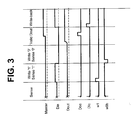
- FIG. 3 A triple-sample destructive read operation on a selected memory cell is illustrated in Figure 3. This illustration indicates that a logic '1' was stored in the selected memory cell 12. An 'X' represents a "don't care" state.
- the data-in and data-out control signals turn off the third and fourth transmission gates 122 and 124, and the two write signals (w1 and w0b) turn off the transistors 128 and 130.
- the first write signal (w1) is pulsed to load a reference '1' in the data-in registers 116, followed by a sense of the reference '1'.
- the second write signal (w0b) is pulsed to load a reference '0' in the data-in registers 116, followed by a sense of the reference '0'.
- the master and slave control signals (Mc and Sc) are held static so that the first and second transmission gates 118 and 120 are off to prevent noise from being generated.
- the data-out control signal (Doc) is pulsed, whereby the outputs of the sense amplifier 22 are stored in the master.
- Data is written back to the memory cells by pulsing the data-in control signal (Dic), whereby the third transmission gate 122 is turned on and the state of the master 112 is stored in the data-in register 116.
- the output (Din) of the data-in register 116 is supplied to the row and column drivers 18 and 20.
- the data is serially shifted.
- the third and fourth transmission gates 122 and 124 are held off, and the master and slave control signals (Mc and Sc) are operated in a synchronous manner to shift data from the masters 112 to the slaves (by pulsing the slave control signal) and then shifting data from the slaves 114 to the masters 112 of the next I/O circuits 24 (by pulsing the master control signal).
- the serial shifting in the I/O circuits is performed until the data in the first I/O circuit 24 has been shifted to the output scan chain port 28. Since the third and fourth transmission gates 122 and 124 are held open, the data that is serially shifted through the I/O circuits 24 does not affect any data that is stored in the data-in registers 116.
- the data-in register 116 allows BIST, write-verify and data balancing to be performed.
- a first order data balancing effort is accomplished by adding a single inverter 132 to the output of every I/O circuit 24.
- the inverter 132 inverts the output (Sout) of the slave 114.
- the inverters 132 of the serially-connected I/O circuits 24 cause data to be inverted as it passes through each I/O circuit 24 and results in a 50/50 ratio of 1's and 0's to be actually written to the memory array when all 1's or all 0's are commanded to be written.
- the inverter 132 of the first circuit will send a '0' to the second circuit
- the inverter 132 of the second I/O circuit 24 will send a '1' to the third I/O circuit 24
- the inverter 132 of the third I/O circuit 24 will send a '0' to the fourth I/O circuit 24, and so on down the scan chain.
- the data balancing is desirable to have the memory physically store roughly an equal number of 1's and 0's. Typical data will contain a majority of 1's or 0's (as in set all or reset all). An equal number of 1's and 0's helps balance the write power requirements and helps avoid the worst case data conditions that may adversely affect sensing reliability.
- An XOR gate 136, a third transistor 138 and a fifth transmission gate 126 are used for write-verify and BIST.
- the third transistors 138 of all of the I/O circuits 24 are wired together to form an OR error flag 140.
- Each XOR gate 136 is enabled by the BIST control signal (Bc).
- a checkerboard pattern is written to the memory array 10, while storing the values in the data-in registers 116.
- the checkerboard pattern is read back by the sense amplifiers 22 and the XOR gates 136 compare the outputs of the sense amplifiers 22 to the values stored values in the data-in registers 116.
- the fifth transmission gates 126 connect the outputs of the XOR gates 136 to the scan chain to give the option of loading the scan chain with the test status of every sense amplifier 22.
- the test control signal (Tc) is pulsed to load the test data into the scan chain and then the scan chain may be operated to shift all of the test data to the scan chain ports 28 or error correction circuitry for a detailed analysis of the test data.
- the error flag 140 signals the controller 26 if an error has been detected in one of the sense amplifiers 22.
- Write-verify is similar to BIST, except that data, not a test pattern, is written to the memory array 10.
- the write-verify operation works as follows: data is shifted from the masters 112 to the data-in registers 116 (the data-in control signal is pulsed), the outputs of the data-in registers (Din) are written to the memory array 10, and sense operations are performed while the data-out control signal (Doc) is kept low (whereby the fourth transmission gate 124 is off). Thus, results of the sense operations are not stored in the masters 112.
- the data-in control signal (Dic) is pulsed to momentarily turn on the third transmission gates 122 to re-load the data in the data-in registers 116 with the original input data from the masters 112.
- the original data is on Din and the sensed data is on Dout.
- the results of the write-verify test provide an indication to the system or error correction control that a write or read problem occurred when writing data, and that corrective action needs to be taken.
- Corrective action may include re-writing and re-verifying, or deciding to recalibrate the write circuits and/or read circuits, or marking the data location as a faulty bit, etc.
- I/O circuit that performs multiple functions, yet is not much larger than a circuit that performs I/O alone. Storing data for write-back is especially advantageous to devices that perform destructive read operations.
- the I/O circuit is not limited to devices that perform destructive read operations. The data balancing, write-verify and built-in self test are useful to other types of memory devices.
Landscapes
- Engineering & Computer Science (AREA)
- Computer Hardware Design (AREA)
- For Increasing The Reliability Of Semiconductor Memories (AREA)
- Read Only Memory (AREA)
- Mram Or Spin Memory Techniques (AREA)
- Semiconductor Memories (AREA)
- Hall/Mr Elements (AREA)
- Tests Of Electronic Circuits (AREA)
- Techniques For Improving Reliability Of Storages (AREA)
Abstract
Description
Claims (9)
- A random access memory device (8) including:an array of memory cells (12);a plurality of drivers (20), each driver (20) corresponding to a slice of the memory cells (12);a plurality of sense amplifiers (22), each sense amplifier (22) corresponding to slice of the memory cells (12); anda plurality of I/O circuits (24), each I/O circuit (24) corresponding to a slice of the memory cells (12), each I/O circuit (24) including a first register (112) having a first output and a first input coupled to an output of the corresponding sense amplifier (22), a second register (116) having a third input coupled to the first output, the third register (116) having a third output coupled to an input of the corresponding driver (20).
- A device as in claim 1, wherein the I/O circuits (24) have serial inputs (Sin) and outputs (Sout) that are connected in a scan chain.
- A device as in claim 2, wherein each I/O circuit (24) includes an inverter (132) between an output of the second register (114) and the serial output (Sout), whereby every other I/O circuit (24) in the scan chain stores an inverted value.
- A device as in claim 1, 2 or 3, wherein each I/O circuit (24) includes a logic gate (136) for comparing data from the corresponding sense amplifier (22) to data stored in the third register (1160, outputs of the logic gates being (136) wired (138) as an OR flag (140).
- A device as in any preceding claim, including a controller (26) for generating global control signals for the I/O circuits.
- A device as in claim 5, wherein each I/O circuit (24) include a first transmission gate (120) for coupling the first output to the second input, and a second transmission gate (122) for coupling the first output to the third input, the control signals causing the first transmission gate (120) to a shift an output of the first register (112) into the second register (114) during a first mode of operation, causing the second transmission gate (122) to shift the output of the first register (122) into the third register (116) during a second mode of operation, and for causing the second transmission gate (122) to isolate the third register (116) during a third mode of operation.
- A device as in claim 5 or 6, wherein each I/O circuit (24) includes means (128, 130) responsive to the controller, for writing directly to the third register.
- A device as in any preceding claim, wherein the sense amplifiers (22) perform destructive read operations.
- A device as in any preceding claim, wherein the device (8) is an MRAM device.
Applications Claiming Priority (2)
| Application Number | Priority Date | Filing Date | Title |
|---|---|---|---|
| US839012 | 2001-04-21 | ||
| US09/839,012 US6587384B2 (en) | 2001-04-21 | 2001-04-21 | Multi-function serial I/O circuit |
Publications (4)
| Publication Number | Publication Date |
|---|---|
| EP1251520A2 true EP1251520A2 (en) | 2002-10-23 |
| EP1251520A3 EP1251520A3 (en) | 2003-07-23 |
| EP1251520B1 EP1251520B1 (en) | 2007-07-25 |
| EP1251520B8 EP1251520B8 (en) | 2007-10-10 |
Family
ID=25278639
Family Applications (1)
| Application Number | Title | Priority Date | Filing Date |
|---|---|---|---|
| EP02252100A Expired - Lifetime EP1251520B8 (en) | 2001-04-21 | 2002-03-22 | Random access memory |
Country Status (7)
| Country | Link |
|---|---|
| US (1) | US6587384B2 (en) |
| EP (1) | EP1251520B8 (en) |
| JP (1) | JP4024582B2 (en) |
| KR (1) | KR100822795B1 (en) |
| CN (1) | CN1332394C (en) |
| DE (1) | DE60221313T2 (en) |
| TW (1) | TW541531B (en) |
Cited By (2)
| Publication number | Priority date | Publication date | Assignee | Title |
|---|---|---|---|---|
| KR100822795B1 (en) * | 2001-04-21 | 2008-04-17 | 삼성전자주식회사 | I / O devices and random access memory devices |
| WO2010077609A1 (en) * | 2008-12-08 | 2010-07-08 | Qualcomm Incorporated | Data integrity preservation in spin transfer torque magnetoresistive random access memory |
Families Citing this family (18)
| Publication number | Priority date | Publication date | Assignee | Title |
|---|---|---|---|---|
| KR100472726B1 (en) | 2002-10-29 | 2005-03-10 | 주식회사 하이닉스반도체 | Semiconductor memory device for high speed data access and method for operating the same |
| US6980455B2 (en) * | 2004-02-03 | 2005-12-27 | Hewlett-Packard Development Company, L.P. | Remote sensed pre-amplifier for cross-point arrays |
| US7042757B2 (en) * | 2004-03-04 | 2006-05-09 | Hewlett-Packard Development Company, L.P. | 1R1D MRAM block architecture |
| FR2877164B1 (en) * | 2004-10-26 | 2007-01-19 | St Microelectronics Sa | ROCKET DEVICE PARTICULARLY OF THE STATE RETENTION TYPE TRIGGERED ON FRONTS |
| US7859069B2 (en) * | 2007-03-16 | 2010-12-28 | Seagate Technology Llc | Magnetic storage element with storage layer magnetization directed for increased responsiveness to spin polarized current |
| JP4994112B2 (en) * | 2007-05-22 | 2012-08-08 | ルネサスエレクトロニクス株式会社 | Semiconductor integrated circuit device and memory control method |
| KR20110100739A (en) * | 2010-03-05 | 2011-09-15 | 삼성전자주식회사 | A method of operating a nonvolatile memory device, a method of operating a controller, and a method of operating a memory system including a nonvolatile memory device and a controller |
| CN102906819B (en) * | 2010-12-16 | 2016-01-06 | 株式会社索思未来 | Semiconductor storage |
| KR20130093394A (en) | 2012-02-14 | 2013-08-22 | 삼성전자주식회사 | A resistive memory device performing a write operation using a multi-mode switching current, a memory system including the same, and a data writing method of the resistive memory device |
| US9875064B2 (en) * | 2015-03-11 | 2018-01-23 | Toshiba Memory Corporation | Storage system architecture for improved data management |
| US10037785B2 (en) * | 2016-07-08 | 2018-07-31 | Micron Technology, Inc. | Scan chain operation in sensing circuitry |
| KR102570472B1 (en) | 2017-01-10 | 2023-08-25 | 에스케이하이닉스 주식회사 | Semiconductor device |
| US10162005B1 (en) | 2017-08-09 | 2018-12-25 | Micron Technology, Inc. | Scan chain operations |
| US11360704B2 (en) * | 2018-12-21 | 2022-06-14 | Micron Technology, Inc. | Multiplexed signal development in a memory device |
| WO2020240227A1 (en) | 2019-05-31 | 2020-12-03 | Micron Technology, Inc. | A memory device architecture coupled to a system-on-chip |
| CN113892144B (en) * | 2019-05-31 | 2025-05-23 | 美光科技公司 | Memory device with improved sensing structure |
| US12254938B2 (en) | 2019-05-31 | 2025-03-18 | Lodestar Licensing Group Llc | Memory device with serial and parallel testing structure for sensing amplifiers |
| US20240420796A1 (en) * | 2023-06-15 | 2024-12-19 | Everspin Technologies, Inc. | Distributed mram configuration bit and method of repair |
Family Cites Families (17)
| Publication number | Priority date | Publication date | Assignee | Title |
|---|---|---|---|---|
| US4495629A (en) * | 1983-01-25 | 1985-01-22 | Storage Technology Partners | CMOS scannable latch |
| JPH071493B2 (en) * | 1987-06-11 | 1995-01-11 | 三菱電機株式会社 | Test auxiliary circuit |
| US5015875A (en) * | 1989-12-01 | 1991-05-14 | Motorola, Inc. | Toggle-free scan flip-flop |
| JP2626920B2 (en) * | 1990-01-23 | 1997-07-02 | 三菱電機株式会社 | Scan test circuit and semiconductor integrated circuit device using the same |
| EP0461923B1 (en) * | 1990-06-15 | 1997-10-01 | Compaq Computer Corporation | True least recently used replacement apparatus |
| USH1796H (en) * | 1996-05-02 | 1999-07-06 | Sun Microsystems, Inc. | Method and circuit for eliminating hold time violations in synchronous circuits |
| US6256224B1 (en) * | 2000-05-03 | 2001-07-03 | Hewlett-Packard Co | Write circuit for large MRAM arrays |
| KR100253565B1 (en) * | 1997-04-25 | 2000-05-01 | 김영환 | Bidirectional Data Input / Output Circuit of Synchronous Memory and Its Control Method |
| KR100275724B1 (en) * | 1997-11-18 | 2000-12-15 | 윤종용 | I / O circuit of high speed semiconductor memory device with reduced test time |
| KR100255664B1 (en) * | 1997-12-29 | 2000-05-01 | 윤종용 | Clock forwarding circuit and clock forwarding method of semiconductor integrated circuit |
| US6292428B1 (en) * | 1998-02-03 | 2001-09-18 | Fujitsu Limited | Semiconductor device reconciling different timing signals |
| KR100301046B1 (en) * | 1998-09-01 | 2001-09-06 | 윤종용 | High speed synchronous memory device having dual ports capable of improving graphic processing speed |
| JP2001093289A (en) * | 1999-09-24 | 2001-04-06 | Nec Corp | Multi-stage read-out circuit and multi-stage read out method |
| US6188615B1 (en) * | 1999-10-29 | 2001-02-13 | Hewlett-Packard Company | MRAM device including digital sense amplifiers |
| JP2001135084A (en) * | 1999-11-08 | 2001-05-18 | Mitsubishi Electric Corp | Semiconductor storage device |
| US6314039B1 (en) * | 2000-05-25 | 2001-11-06 | Hewlett-Packard Company | Characterization of sense amplifiers |
| US6587384B2 (en) * | 2001-04-21 | 2003-07-01 | Hewlett-Packard Development Company, L.P. | Multi-function serial I/O circuit |
-
2001
- 2001-04-21 US US09/839,012 patent/US6587384B2/en not_active Expired - Lifetime
- 2001-12-25 TW TW090132234A patent/TW541531B/en not_active IP Right Cessation
-
2002
- 2002-02-21 CN CNB021051364A patent/CN1332394C/en not_active Expired - Lifetime
- 2002-03-22 EP EP02252100A patent/EP1251520B8/en not_active Expired - Lifetime
- 2002-03-22 DE DE60221313T patent/DE60221313T2/en not_active Expired - Lifetime
- 2002-04-19 JP JP2002117035A patent/JP4024582B2/en not_active Expired - Fee Related
- 2002-04-20 KR KR1020020021796A patent/KR100822795B1/en not_active Expired - Fee Related
Cited By (3)
| Publication number | Priority date | Publication date | Assignee | Title |
|---|---|---|---|---|
| KR100822795B1 (en) * | 2001-04-21 | 2008-04-17 | 삼성전자주식회사 | I / O devices and random access memory devices |
| WO2010077609A1 (en) * | 2008-12-08 | 2010-07-08 | Qualcomm Incorporated | Data integrity preservation in spin transfer torque magnetoresistive random access memory |
| US8159864B2 (en) | 2008-12-08 | 2012-04-17 | Qualcomm Incorporated | Data integrity preservation in spin transfer torque magnetoresistive random access memory |
Also Published As
| Publication number | Publication date |
|---|---|
| US20020154536A1 (en) | 2002-10-24 |
| KR100822795B1 (en) | 2008-04-17 |
| TW541531B (en) | 2003-07-11 |
| KR20030009109A (en) | 2003-01-29 |
| DE60221313D1 (en) | 2007-09-06 |
| JP4024582B2 (en) | 2007-12-19 |
| JP2003007049A (en) | 2003-01-10 |
| DE60221313T2 (en) | 2008-04-03 |
| EP1251520B8 (en) | 2007-10-10 |
| CN1383154A (en) | 2002-12-04 |
| EP1251520B1 (en) | 2007-07-25 |
| CN1332394C (en) | 2007-08-15 |
| EP1251520A3 (en) | 2003-07-23 |
| US6587384B2 (en) | 2003-07-01 |
Similar Documents
| Publication | Publication Date | Title |
|---|---|---|
| EP1251520B1 (en) | Random access memory | |
| EP1349171B1 (en) | Data exchange device between scan chains | |
| CA2649002A1 (en) | A program verify method for otp memories | |
| CN113963739A (en) | Fuse circuit with reduced footprint | |
| US4326290A (en) | Means and methods for monitoring the storage states of a memory and other storage devices in a digital data processor | |
| TW594777B (en) | Memory circuit having compressed testing function | |
| US7085171B2 (en) | Semiconductor memory device | |
| US10541041B2 (en) | Semiconductor device | |
| JPH09115298A (en) | Semiconductor memory device | |
| US6701470B1 (en) | Method for testing a memory device having different number of data pads than the tester | |
| US5369752A (en) | Method and apparatus for shifting data in an array of storage elements in a data processing system | |
| US9870810B2 (en) | Method and system for power signature suppression in memory devices | |
| KR100364830B1 (en) | Memory test circuit | |
| US6611929B1 (en) | Test circuit for memory | |
| US20100124141A1 (en) | Semiconductor memory device of dual-port type | |
| JP2604468B2 (en) | Semiconductor integrated circuit device | |
| US20150213883A1 (en) | Testing signal development on a bit line in an sram | |
| CN110751975B (en) | Memory device and test circuit thereof | |
| KR100596821B1 (en) | Memory devices that support multiprocessor functionality | |
| WO2009058148A1 (en) | Mram testing | |
| US9715944B1 (en) | Automatic built-in self test for memory arrays | |
| US12584961B2 (en) | Built-in self test circuit for segmented static random access memory (SRAM) array input/output | |
| CN112053729A (en) | Memory device and method of operating the same | |
| US7743291B2 (en) | Semiconductor memory device | |
| KR100490647B1 (en) | Method for testing semiconductor memory device with tag block |
Legal Events
| Date | Code | Title | Description |
|---|---|---|---|
| PUAI | Public reference made under article 153(3) epc to a published international application that has entered the european phase |
Free format text: ORIGINAL CODE: 0009012 |
|
| AK | Designated contracting states |
Kind code of ref document: A2 Designated state(s): AT BE CH CY DE DK ES FI FR GB GR IE IT LI LU MC NL PT SE TR |
|
| AX | Request for extension of the european patent |
Free format text: AL;LT;LV;MK;RO;SI |
|
| PUAL | Search report despatched |
Free format text: ORIGINAL CODE: 0009013 |
|
| AK | Designated contracting states |
Designated state(s): AT BE CH CY DE DK ES FI FR GB GR IE IT LI LU MC NL PT SE TR |
|
| AX | Request for extension of the european patent |
Extension state: AL LT LV MK RO SI |
|
| RIC1 | Information provided on ipc code assigned before grant |
Ipc: 7G 11C 11/16 A Ipc: 7G 11C 29/00 B Ipc: 7G 11C 7/10 B |
|
| 17P | Request for examination filed |
Effective date: 20040120 |
|
| AKX | Designation fees paid |
Designated state(s): DE GB |
|
| GRAP | Despatch of communication of intention to grant a patent |
Free format text: ORIGINAL CODE: EPIDOSNIGR1 |
|
| RAP1 | Party data changed (applicant data changed or rights of an application transferred) |
Owner name: HEWLETT-PACKARD COMPANY |
|
| GRAS | Grant fee paid |
Free format text: ORIGINAL CODE: EPIDOSNIGR3 |
|
| GRAA | (expected) grant |
Free format text: ORIGINAL CODE: 0009210 |
|
| AK | Designated contracting states |
Kind code of ref document: B1 Designated state(s): DE GB |
|
| REG | Reference to a national code |
Ref country code: GB Ref legal event code: FG4D |
|
| RAP2 | Party data changed (patent owner data changed or rights of a patent transferred) |
Owner name: SAMSUNG ELECTRONICS CO., LTD. |
|
| REF | Corresponds to: |
Ref document number: 60221313 Country of ref document: DE Date of ref document: 20070906 Kind code of ref document: P |
|
| PLBE | No opposition filed within time limit |
Free format text: ORIGINAL CODE: 0009261 |
|
| STAA | Information on the status of an ep patent application or granted ep patent |
Free format text: STATUS: NO OPPOSITION FILED WITHIN TIME LIMIT |
|
| 26N | No opposition filed |
Effective date: 20080428 |
|
| PGFP | Annual fee paid to national office [announced via postgrant information from national office to epo] |
Ref country code: DE Payment date: 20210217 Year of fee payment: 20 Ref country code: GB Payment date: 20210219 Year of fee payment: 20 |
|
| REG | Reference to a national code |
Ref country code: DE Ref legal event code: R071 Ref document number: 60221313 Country of ref document: DE |
|
| REG | Reference to a national code |
Ref country code: GB Ref legal event code: PE20 Expiry date: 20220321 |
|
| PG25 | Lapsed in a contracting state [announced via postgrant information from national office to epo] |
Ref country code: GB Free format text: LAPSE BECAUSE OF EXPIRATION OF PROTECTION Effective date: 20220321 |
|
| P01 | Opt-out of the competence of the unified patent court (upc) registered |
Effective date: 20230520 |