EP1245971A2 - Waveguide taper with lateral rib confinement waveguides - Google Patents
Waveguide taper with lateral rib confinement waveguides Download PDFInfo
- Publication number
- EP1245971A2 EP1245971A2 EP02076214A EP02076214A EP1245971A2 EP 1245971 A2 EP1245971 A2 EP 1245971A2 EP 02076214 A EP02076214 A EP 02076214A EP 02076214 A EP02076214 A EP 02076214A EP 1245971 A2 EP1245971 A2 EP 1245971A2
- Authority
- EP
- European Patent Office
- Prior art keywords
- waveguide
- rib
- waveguides
- slab
- tapered
- Prior art date
- Legal status (The legal status is an assumption and is not a legal conclusion. Google has not performed a legal analysis and makes no representation as to the accuracy of the status listed.)
- Granted
Links
Images




Classifications
-
- G—PHYSICS
- G02—OPTICS
- G02B—OPTICAL ELEMENTS, SYSTEMS OR APPARATUS
- G02B6/00—Light guides; Structural details of arrangements comprising light guides and other optical elements, e.g. couplings
- G02B6/10—Light guides; Structural details of arrangements comprising light guides and other optical elements, e.g. couplings of the optical waveguide type
- G02B6/12—Light guides; Structural details of arrangements comprising light guides and other optical elements, e.g. couplings of the optical waveguide type of the integrated circuit kind
- G02B6/122—Basic optical elements, e.g. light-guiding paths
- G02B6/1228—Tapered waveguides, e.g. integrated spot-size transformers
-
- H—ELECTRICITY
- H01—ELECTRIC ELEMENTS
- H01S—DEVICES USING THE PROCESS OF LIGHT AMPLIFICATION BY STIMULATED EMISSION OF RADIATION [LASER] TO AMPLIFY OR GENERATE LIGHT; DEVICES USING STIMULATED EMISSION OF ELECTROMAGNETIC RADIATION IN WAVE RANGES OTHER THAN OPTICAL
- H01S5/00—Semiconductor lasers
- H01S5/20—Structure or shape of the semiconductor body to guide the optical wave ; Confining structures perpendicular to the optical axis, e.g. index or gain guiding, stripe geometry, broad area lasers, gain tailoring, transverse or lateral reflectors, special cladding structures, MQW barrier reflection layers
- H01S5/22—Structure or shape of the semiconductor body to guide the optical wave ; Confining structures perpendicular to the optical axis, e.g. index or gain guiding, stripe geometry, broad area lasers, gain tailoring, transverse or lateral reflectors, special cladding structures, MQW barrier reflection layers having a ridge or stripe structure
-
- G—PHYSICS
- G02—OPTICS
- G02B—OPTICAL ELEMENTS, SYSTEMS OR APPARATUS
- G02B6/00—Light guides; Structural details of arrangements comprising light guides and other optical elements, e.g. couplings
- G02B6/10—Light guides; Structural details of arrangements comprising light guides and other optical elements, e.g. couplings of the optical waveguide type
- G02B6/12—Light guides; Structural details of arrangements comprising light guides and other optical elements, e.g. couplings of the optical waveguide type of the integrated circuit kind
- G02B2006/12083—Constructional arrangements
- G02B2006/12097—Ridge, rib or the like
-
- H—ELECTRICITY
- H01—ELECTRIC ELEMENTS
- H01S—DEVICES USING THE PROCESS OF LIGHT AMPLIFICATION BY STIMULATED EMISSION OF RADIATION [LASER] TO AMPLIFY OR GENERATE LIGHT; DEVICES USING STIMULATED EMISSION OF ELECTROMAGNETIC RADIATION IN WAVE RANGES OTHER THAN OPTICAL
- H01S5/00—Semiconductor lasers
- H01S5/10—Construction or shape of the optical resonator, e.g. extended or external cavity, coupled cavities, bent-guide, varying width, thickness or composition of the active region
- H01S5/1053—Comprising an active region having a varying composition or cross-section in a specific direction
- H01S5/1064—Comprising an active region having a varying composition or cross-section in a specific direction varying width along the optical axis
-
- H—ELECTRICITY
- H01—ELECTRIC ELEMENTS
- H01S—DEVICES USING THE PROCESS OF LIGHT AMPLIFICATION BY STIMULATED EMISSION OF RADIATION [LASER] TO AMPLIFY OR GENERATE LIGHT; DEVICES USING STIMULATED EMISSION OF ELECTROMAGNETIC RADIATION IN WAVE RANGES OTHER THAN OPTICAL
- H01S5/00—Semiconductor lasers
- H01S5/40—Arrangement of two or more semiconductor lasers, not provided for in groups H01S5/02 - H01S5/30
- H01S5/4025—Array arrangements, e.g. constituted by discrete laser diodes or laser bar
- H01S5/4031—Edge-emitting structures
Definitions
- This invention relates to integrated semiconductor devices and methods of making the same.
- the invention relates to devices incorporating optical waveguide structures as well as methods of manufacturing the same.
- An integrated optical circuit employs optical waveguides to implement devices, such as optical transmitters and receivers, switches and couplers. Waveguides also efficiently transmit light through the optical circuit and connect to external optical waveguides such as optical fibers, generally butt-coupled to the device.
- devices such as optical transmitters and receivers, switches and couplers.
- Waveguides also efficiently transmit light through the optical circuit and connect to external optical waveguides such as optical fibers, generally butt-coupled to the device.
- external optical waveguides such as optical fibers, generally butt-coupled to the device.
- the former has typically a 1-2 ⁇ m elliptical modal spot, which is neither well-sized nor shaped to match the standard 8-9 ⁇ m circular modal spot of conventional single-mode optical fibers.
- This invention aims to provide a widened output mode semiconductor optical device, which is simple to implement, is easy to fabricate and which results in only low losses of light.
- This invention also aims to provide a method of manufacture of a widened output mode semiconductor optical device, which is simple to implement, is easy to fabricate and which results in only low losses of light.
- the invention provides a waveguide component having a slab waveguide, a rib waveguide, and a mode transition section where the rib waveguide and the slab waveguide are adjacent, and where the rib waveguide is tapered, to provide optical coupling, and lateral confinement waveguides are provided along the slab waveguide in the mode transition section to confine light from spreading laterally.
- the lateral waveguides may also be rib waveguides.
- a rib waveguide preferably comprises a lower confinement layer having a first refractive index, a core layer having a second refractive index which is higher than the surrounding materials, an upper cladding layer having a refractive index lower than the index of the core, and a material that generally flanks the core and the cladding layers.
- the material of the upper cladding layer is the same as the lower confinement layer.
- the material flanking the cladding and the core may be the same as the cladding.
- the rib core is buried in the material that forms the cladding and the surrounding material.
- the lateral confinement rib waveguides are significant for enabling a mode transition section which couples with low loss, which reduces the fabrication difficulties of prior art arrangements, and is easy to implement. In particular, it reduces the need for the taper to be very fine, or the taper to be made in both vertical and horizontal axes, both of which cause fabrication difficulties.
- the lateral confinement ribs can be formed in the same plane as the tapered rib, they can be formed coaxially and along both sides of the tapered rib, they can be formed on the slab, they can be formed in the same manufacturing step as the tapered rib. If the same manufacturing step is used, there is no need for difficult precise alignment of separate steps, if a single mask is used for example.
- the tapered rib can be shaped so that the tapering becomes finer as the rib gets narrower.
- the slab waveguide can have vertical confinement by an antiresonant reflection layer having a refractive index higher than a core of the slab waveguide.
- a rib waveguide grown on a slab waveguide the width of the rib waveguide decreasing in a mode transition section in which said rib waveguide is sided by two sets of confinement waveguides, grown in the same fabrication step as the central rib waveguide.
- the decrease in the central rib waveguide results in the coupling of its optical mode to a wider mode guided by the slab waveguide and laterally confined by the influence of the lateral waveguides.
- a tapered rib waveguide comprising:
- aspects of the invention include methods of manufacturing the waveguide component, and applications to optical components such as semiconductor lasers, waveguide arrays for filtering, for dispersion compensation, for wavelength division multiplexing/demultiplexing, and switching, and arrays of receivers for example.
- optical components such as semiconductor lasers, waveguide arrays for filtering, for dispersion compensation, for wavelength division multiplexing/demultiplexing, and switching, and arrays of receivers for example.
- wavelength division multiplexed systems there may be tens or hundreds or more of optical paths, and so providing compact and less expensive interfaces to integrated waveguide components can be commercially valuable.
- Other suitable applications are semiconductor optical amplifiers, optical regenerators, optical filters, optical splitters.
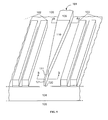
- a first embodiment of the invention illustrated in transverse and longitudinal perspective in FIG. 1 and 2, respectively, is a semiconductor buried waveguide 1 surrounded by a set of two straight semiconductor buried waveguides 2, 3 along its tapered region 10. All of them are defined adjacent, in this example over, a slab waveguide 4.
- the invention comprises a vertical series of horizontal semiconductor layers which constitute the following elements.
- a slab passive waveguide 4 To enable it to guide optical waves, this waveguide 4 has a refractive index which is greater than the refractive index of the surrounding materials 5, 6. This slab waveguide 4 may be also defined over the tapered waveguide 1 and the lateral waveguides 2, 3.
- This separating layer 6 may have a thickness in a range from 0 to a few microns. This thickness can be 0 microns when the slab waveguide 4 does not influence the guiding function of the tapered waveguide 1 or can improve this guiding function.
- a buried waveguide 1 which can be either active or passive.
- the tapered waveguide When the tapered waveguide is active it may be constituted either by a number of active quantum wells and barriers or by bulk active material, but this is not critical to the invention.
- the material in which the central waveguide 1 is buried 7 may be the same as the lower confinement layer 5 and the separating layer 6.
- the material of this cladding layer 7 is usually the same as the lower confinement layer 5 and the separating layer 6.
- All the layers have a substantially constant height and thickness along the invention.
- the present invention is applied to active components such as semiconductor lasers or semiconductor amplifiers, every layer requires an electrical doping for an efficient injection of carriers into the active central waveguide.
- active components such as semiconductor lasers or semiconductor amplifiers
- the well-known complementary materials that the operation of the laser needs such as electrical confinement layers, contact layers, insulator layer 8 and electrodes, are not shown.
- passive components the typical material 8 over the cladding layer 7 is air.
- the central tapered rib 1 tapers from a width W i 9 to a final width W f 11.
- the initial width W i may be the width of a standard monomode waveguide 9, and it will depend on the materials used in the fabrication of the present invention. In case the present invention is used integrated in a semiconductor laser, the width W i 9 will be the optimum width that provides the best lasing performance.
- the final width W f is narrow enough in order to provoke the total light transfer form the central waveguide 1 to the slab waveguide 4. It may be useful, to define a straight section 11 at the end of the tapered waveguide, having a width W f . Said final section 11 provides a safety section in case the device has to be cleaved at the end of the tapered section 10.
- the shape of the tapered section 10 can follow any mathematical function, such as linear, exponential or parabolic. It is desired that said shape provides low transformation losses when spreading the light propagated by the central waveguide 1, to the adjacent slab waveguide 4.
- the width that the central rib 1 has in its narrow final section W f must be both fine enough to ensure the entire guidance of the light by the underlying broad leaky mode and wide enough to avoid the difficulties of fabricating very narrow sections. Typical values are in the range 0.6-0.3 microns.
- the lateral sets of buried waveguides 2, 3 may be defined along each side of the tapered waveguide section 10 and their dimensions and location may be symmetric with respect to the central tapered waveguide 1.
- the number of lateral waveguides 2, 3, the widths of each lateral waveguide 2, 3 and the gaps between them should be designed in order to provide the lateral confinement of the mode of the slab waveguide 4.
- the technological requirements for the definition of the widths of the lateral waveguides 2, 3 and the gaps between them are not critical.
- the typical configuration of the lateral waveguides 2, 3 is a periodic patterning of straight waveguides, with constant widths and gaps, but this is not a requirement for the present invention. They may present irregular and different widths and gaps, or even varying widths and gaps along its length. Typical values for the width of straight lateral waveguides 2, 3 and gap between them lay around the range 0.5-2 and 1-3 microns, respectively.
- a typical number of lateral waveguides in each side of the central tapered waveguide 1 is 3.
- the gap between the inner rib waveguides of each group of lateral ribs 2, 3, is defined in order to provide high coupling efficiency to, for example, a single mode fiber.
- a typical value is in the range 5-10 microns.
- the lateral waveguides 2, 3 may be patterned (e.g. photolithography followed by etching) in the same fabrication step as the central waveguide 1. In this case the fabrication of the device is considerably simplified.
- the optical field of the fundamental modes is preferably calculated for light propagating in various portions of the illustrated tapered waveguide 1.
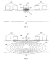
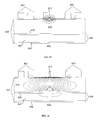
- the contour lines for the electrical field are illustrated in FIG. 3 for the central rib 1 having a width of W i and in FIG. 4 for the central rib 1 having a width of W f .
- Each illustrated contour line represents a 10 % of the maximum intensity decrease.
- the mode 12 is tightly confined to the central buried waveguide 1 when its width is W i .
- W f For the width of the central waveguide 1 being W f the light spreads 13 in the slab waveguide 4 and its surrounding layers 5, 6.
- the influence of the lateral pairs of straight ribs 2, 3 causes the light traveling in the slab waveguide 4 to be confined laterally.
- the vertical confinement of the broadened slab mode 13 is provided by the slab waveguide defined by the slab core 4 and the surrounding materials, that is, the lower confinement layer 5 and the separating layer 6.
- the lateral confinement provided by the two couples of ribs 2, 3 is provided by a resonant tunneling phenomenon produced between the slab 4 fundamental mode and the modes of the lateral sets of buried waveguides 2, 3.
- the formed mode 13 leaks energy through the slab core 4 because it does not use total internal reflection in its lateral boundaries, but the power lost along the device is negligible compared to the modal transformation loss.
- Typical values in one illustrative example in an InP substrate for the first embodiment are shown in table 1: Part Material Refractive Index Thickness (microns) Air 1.0 Insulator Polyimide 1.7 Cladding layer InP 3.17 2.35 Buried waveguides and InGaAsP lateral waveguides (Bulk) 3.6 0.35 Separating layer InP 3.17 0.3 Slab waveguide InGaAsP 3.388 0.04 Lower confinement layer InP 3.17
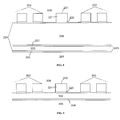
- a second embodiment of the invention is illustrated in perspective in FIG. 5. Its behavior is similar to the first embodiment. It therefore comprises elements implementing the same functions, referred to by the same terminology, and any information given hereinabove remains valid unless otherwise indicated. If an element of the second embodiment has the same function as an element of the first embodiment it is identified hereinafter by the same reference number increased by 100.
- a tapered rib waveguide 101 surrounded by a two set of lateral rib waveguides 102, 103 along its tapered region and defined over a slab waveguide 104 is illustrated.
- a first lower confinement layer 105 having a first refractive index As in the first embodiment, a first lower confinement layer 105 having a first refractive index.
- a slab core layer 104 To enable it to guide optical waves, this waveguide 104 has a refractive index which is greater than the refractive index of the lower confinement layer 105.
- a central tapered rib waveguide 101 comprising a core layer 120 and a cladding layer 121 and flanked in the transverse direction by a complementary material 108.
- the complementary material 108 that flanks the central 101 and the lateral waveguides 102, 103 may be air when the present invention is integrated with passive devices and so the core of the rib waveguides 101, 102, 103 is passive.
- the complementary material 108 might be an insulator, such as polyimide. In this case, the well known complementary materials that the operation of a laser or active component needs, are not shown.
- the lateral ribs 102, 103 may be defined in the same technological step as the central one 101. In that case the fabrication is again drastically simplified.
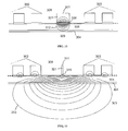
- the optical field of the fundamental mode of the tapered rib 101 is calculated in the straight section of the taper 109 and at the end section of the taper 111.
- the mode 112 is tightly confined to the upper rib 101 when it is W i wide.
- the rib being W f the light spreads 113 in the slab waveguide 4.
- the influence of the lateral pairs of straight ribs 102, 103 causes the light traveling in the slab waveguide 104 to be confined laterally.
- Typical values in one illustrative example in an InP substrate for the second embodiment are shown in table 2: Part Material Refractive Index Thickness (microns) Air 1.0 Insulator Polyimide 1.7 Cladding layer InP 3.17 1.5 Core of the central and InGaAsP lateral rib waveguides (QW's) 3.41 0.2 Slab waveguide InGaAsP 3.19 4 Lower confinement layer InP 3.17
- a third embodiment of the invention is illustrated in the cross-section view of FIG. 8. Its behavior is identical to the second embodiment. It therefore comprises elements implementing the same functions, referred to by the same terminology, and any information given hereinabove remains valid unless otherwise indicated. If an element of the third embodiment has the same function as an element of the second embodiment it is identified hereinafter by the same reference number increased by 100.
- the slab core layer 204 may have the same refractive index as the lower confinement layer 205.
- an antiresonant reflecting element 223 may be used to provide the vertical confinement of the fundamental mode of the slab waveguide 224 (see "Antiresonant reflecting optical waveguides for III-V integrated optics" by T. L. Koch, U. Koren, G. D. Boyd, P. J. Corvini and M. A. Duguay, Electron. Let., Vol. 33, no. 5, February 1987 or EP 228886A2) in combination with the tapered central rib waveguide 201 and the lateral waveguides that provide the lateral confinement 202, 203.
- the antiresonant reflecting element 223 may comprise a stack of horizontal layers of different refractive indexes 225, 226, 227 in order to provide constructive interference to the propagated fundamental mode and provide its confinement. There is some amount of light leaking towards the lower confinement layer 205 but it remains negligible compared to the mode transformation losses of the invention.
- Typical materials and values for the antiresonant reflecting element layers are shown in table 3: Layer Material Refractive Index Thickness (microns) Central antiresonant layer 225 InP 3.17 1.5 First antiresonant layer 226 InGaAsP 3.39 0.3 Third antiresonant layer 227 InGaAsP 3.39 0.3
- FIG. 1 and FIG. 5 can be combined as illustrated in the cross-section view of FIG. 9. Its behavior is generally identical to the second embodiment. It therefore comprises elements implementing the same functions, referred to by the same terminology, and any information given hereinabove remains valid unless otherwise indicated. If an element of the fourth embodiment has the same function as an element of the second embodiment it is identified hereinafter by the same reference number increased by 200.
- a tapered rib waveguide 301 surrounded by a two set of lateral rib waveguides 302, 303 along its tapered region and defined over a slab waveguide 304 is illustrated.
- the succession of horizontal functional layers and the elements they constitute are as follows:
- a lower confinement layer 305 having a first refractive index having a first refractive index.
- a slab passive waveguide 304 To enable it to guide optical waves, this waveguide 304 has a refractive index which is greater than the refractive index of the surrounding materials 305, 306.
- a separating layer 306 that in most cases is the same material as the lower confinement layer 305.
- This separating layer 306 may have a thickness in a range from 0 to a few microns. This thickness can be 0 microns when the slab waveguide 4 does not influence the guiding function of the tapered waveguide 301 or can improve this guiding function.
- a central tapered rib waveguide 301 comprising a core layer 320 and a cladding layer 321 and flanked in the transverse direction by a complementary material 308.
- Two sets of lateral rib waveguides 302, 303 surrounding the central tapered rib waveguide 301 and flanked by the same material 308 as the central tapered waveguide 301 is.
- the present embodiment is identical to the second embodiment. Using the separating layer 306 and an appropriate thickness of the slab waveguide core 304 it is possible to obtain broader output modes which are well confined by the lateral rib waveguides 302, 303.
- the optical field of the fundamental mode of the tapered rib 301 is calculated in the straight section of the taper and at the end section of the taper.
- the mode 112 is tightly confined to the upper rib 301 when it is W i wide.
- the rib being W f the light spreads 313 in the slab waveguide 304.
- the influence of the lateral pairs of straight ribs 302, 303 causes the light traveling in the slab waveguide 4 to be confined laterally.
- Typical values in one illustrative example in an InP substrate for the first embodiment are shown in table 4: Part Material Refractive Index Thickness (microns) Air 1.0 Insulator Polyimide 1.7 Cladding layer InP 3.17 1.5 Core of the central and InGaAsP lateral rib waveguides (QW's) 3.41 0.2 Separating layer InP 3.17 1 Slab waveguide InGaAsP 3.23 0.2 Lower confinement layer InP 3.17
- a fifth embodiment of the invention is a tapered rib waveguide 401 surrounded by a set of two straight rib waveguides 402, 403 along its tapered region 414, 415, all of them grown over a thick slab waveguide 404.
- the thick slab waveguide 404 may have a core layer 410 with a refractive index lower than the core of the upper rib waveguides 411.
- a substrate 405 of InP may be used for subsequent epitaxial growth.
- An antiresonant reflecting element 406 may be first deposited as a vertical confinement layer, comprising a layer of InP of suitable thickness such as 1.84 ⁇ m of thickness 407, which is sandwiched by two layers of InGaAsP Q(1.3) of 0.32 ⁇ m each one 408, 409.
- the purpose of said antiresonant reflecting element 406 is to provide the vertical confinement of the slab mode excited at the output of the taper 416 (see "Antiresonant reflecting optical waveguides for III-V integrated optics" by T. L. Koch, U. Koren, G. D. Boyd, P. J. Corvini and M. A. Duguay, Electron. Let., Vol. 33, no. 5, February 1987).
- the slab waveguide core layer 410 of InP is deposited to a thickness of 3.5 ⁇ m.
- an active core layer 411 to generate and guide the light in the upper central rib waveguide may be grown to a thickness of 180 nm.
- the active layer consists of five 1% compressively strained 80 ⁇ -thick In 0.778 Ga 0.222 As 0.7874 P 0.2126 quantum wells (QW's) for emission at 1.55 ⁇ m, and four lattice matched 150 ⁇ -thick In 0.751 G 0.249 As 0.5393 P 0.4607 barriers, surrounded by 400 ⁇ -thick separate confinement heterostrucutre (SCH) regions.
- QW's quantum wells
- a cladding layer 412 of InP On top is deposited a cladding layer 412 of InP to a thickness of 1.5 ⁇ m.
- the rib waveguides 401, 402, 403 are then patterned, e.g. photolithographically followed by etching the cladding and the upper core layers up to 1.54 ⁇ m. The light generating QW's layers are not reached.
- Every layer requires an electrical doping for an efficient injection of carriers into the active central waveguide.
- the well-known complementary materials that the operation of the laser needs such as electrical confinement layers, contact layers, insulator layer and electrodes, are not shown.
- the central rib has three sections, a wide rib 413, a narrow rib 415 and a taper 414 connecting the two.
- the wide rib 413 where the light generation is produced, has a width of 3 ⁇ m.
- the narrow rib 415 has a width of 0.3 ⁇ m.
- the taper 414 consists of a piecewise linear device consisting of three linear sections.
- the two lateral pairs of straight rib waveguides 402, 403 are defined along each side of the tapered 414 and narrow 415 sections of the central rib 401 and their dimensions and location are symmetric with respect to the central tapered guide 401. They have a width of 1.5 ⁇ m and a gap of 1 ⁇ m between the ribs of the same pair.
- the gap between the inner rib waveguides of each group, where the central rib is implemented, is 8 ⁇ m.
- the refractive indexes for these materials are shown in Table 5.
- Part Material Refractive Index Air 1.0 Insulator Polyimide 1.7
- Upper cladding InP 3.17 Active core (equivalent index) (QW's) 3.42
- Substrate InP 3.17 The upper faces of the ribs 1, 2, 3 and slab waveguides 4 are substantially parallel to the plane of a chip, i.e. the ribs and the slab core each have a substantially constant height and thickness above the surface of the chip.
- the optical field of the fundamental modes is preferably calculated for light propagating in various portions of the illustrated tapered waveguide 401.
- the light is preferably assumed to have a free-space wavelength of 1.55 ⁇ m, typically used in optical communication applications.
- the contour lines for the electrical field are illustrated in FIG. 13 for the wide central rib 413 and in FIG. 14 for the narrow central rib 415. Each illustrated contour line represents a 10 % of the maximum intensity decrease.
- the mode 417 is tightly confined to the upper rib 401 when it is 3 ⁇ m wide.
- the light spreads 418 in the thicker slab waveguide 404.
- the influence of the lateral pairs of straight ribs 402, 403 causes the light traveling in the slab waveguide 404 to be confined laterally.
- the vertical confinement of the broadened slab mode 418 is provided by the antiresonant character of the lower layers 406 of the structure relative to the component of propagation normal to the layers.
- the lateral confinement provided by the two couples of ribs 402, 403 is provided by a resonant tunneling phenomenon produced between the slab 4 modes and the upper rib 402, 403 modes.
- the formed mode 418 leaks energy through the substrate and the slab core 410 because it does not use total internal reflection in three of its four transversal boundaries, but the power lost along the device is negligible compared to the modal transformation loss.
- FIG. 15 A further embodiment of the invention is illustrated in the cross-section view of FIG. 15. Its behavior is generally identical to the previous embodiment. It therefore comprises elements implementing the same functions, referred to by the same terminology, and any information given hereinabove remains valid unless otherwise indicated. If an element of the this laser has the same function as an element of the previous layer it is identified hereinafter by the same reference number increased by 100.
- a substrate of InP 105 has a refractive index of 3.17.
- a slab core layer 510 of In 0.97 Ga 0.03 As 0.064 P 0.936 with a refractive index of 3.19 and 4 ⁇ m thick is the next grown layer.
- the upper rib core layer 511 consists of Q(1.2) over a thickness of 0.4 ⁇ m and with an index of 3.33.
- the final cladding of InP 512 is grown over 0.5 ⁇ m.
- a following etching process defines the central tapered rib waveguide 501 and the two sets of 3 straight ribs 502, 503 in a height of 0.65 ⁇ m.
- the structure described in this embodiment is a passive device designed to work at wavelengths of 1.55 ⁇ m hence the layers do not need either an electrical doping or confinement layers or contact layers or insulator layer or electrodes.
- the two lateral sets of straight ribs 502, 503, which extend along the tapered section of the central waveguide, are separated 8 ⁇ m and have a gap of 1 ⁇ m between each pair of ribs.
- the central rib waveguide 501 adiabatically tapers from a section where it is 2 ⁇ m wide to another section where the width of the rib is 0.3 ⁇ m.
- This embodiment does not make use of an antiresonance condition to vertically confine the broad slab mode.
- the means for vertical confinement is provided by the refractive index of the slab core which assures this vertical confinement.
- the lateral two sets of straight ribs 502, 503 implement the same function as hereinabove, but due to the thicker slab core 510 three ribs are needed to reduce the leaky losses and realize an efficient lateral confinement.
- In InP technology however, it is necessary to grow low Ga and As fraction quaternary materials to get the low refractive indexes needed by the slab core 510, and in fact, they are rather difficult to grow.
- This problem can be overcome using the same InP slab core 510 and antiresonance vertical cladding as hereinabove or alternatively growing layers of InP and quaternary materials with higher Ga and As fractions, and thus higher refractive index, to implement a diluted core with an equivalent index as desired.
- the width that the central rib 501 has in its narrow section must be both fine enough to ensure the entire guidance of the light by the underlying broad leaky mode and wide enough to avoid the difficulties of fabricating very narrow sections.
- the previous embodiments comprise a piecewise linear taper consisting of a certain number of sections, e.g. three linear sections. Nevertheless, in some circumstances, it may be desirable to form a similar structure on a gradually curving waveguide.
- the shape of the rib in the taper section does not need to be straight but may also be curved.
- the semiconductor materials are indium gallium arsenide phosphide (InGaAsP), but other semiconductor materials are also in the scope of the invention.
- the active material type includes bulk material or quantum wells, but again this is not critical to the invention.
- the fabrication method presently contemplated is metal-organic chemical vapor deposition (MOCVD), but liquid phase epitaxy (LPE), molecular beam epitaxy (MBE) and other chemical vapor deposition techniques may also be employed.
- MOCVD metal-organic chemical vapor deposition
- LPE liquid phase epitaxy
- MBE molecular beam epitaxy
- the etching of the ribs may be performed by standard wet chemical etching or by reactive ion etching or other etching techniques.
- the invention thus provides a simple and very easily fabricated optical device that provides efficient mode size and shape transformation and significant fiber coupling improvements.
Landscapes
- Physics & Mathematics (AREA)
- General Physics & Mathematics (AREA)
- Optics & Photonics (AREA)
- Engineering & Computer Science (AREA)
- Geometry (AREA)
- Condensed Matter Physics & Semiconductors (AREA)
- Electromagnetism (AREA)
- Power Engineering (AREA)
- Microelectronics & Electronic Packaging (AREA)
- Optical Integrated Circuits (AREA)
- Waveguide Aerials (AREA)
Abstract
Description
In another aspect of the present invention a tapered rib waveguide is provided, comprising:
| Part | Material | Refractive Index | Thickness (microns) |
| Air | 1.0 | ||
| Insulator | Polyimide | 1.7 | |
| Cladding layer | InP | 3.17 | 2.35 |
| Buried waveguides and | InGaAsP | ||
| lateral waveguides | (Bulk) | 3.6 | 0.35 |
| Separating layer | InP | 3.17 | 0.3 |
| Slab waveguide | InGaAsP | 3.388 | 0.04 |
| Lower confinement layer | InP | 3.17 |
| Part | Material | Refractive Index | Thickness (microns) |
| Air | 1.0 | ||
| Insulator | Polyimide | 1.7 | |
| Cladding layer | InP | 3.17 | 1.5 |
| Core of the central and | InGaAsP | ||
| lateral rib waveguides | (QW's) | 3.41 | 0.2 |
| Slab waveguide | InGaAsP | 3.19 | 4 |
| Lower confinement layer | InP | 3.17 |
| Layer | Material | Refractive Index | Thickness (microns) |
| Central | InP | 3.17 | 1.5 |
| First | InGaAsP | 3.39 | 0.3 |
| Third | InGaAsP | 3.39 | 0.3 |
| Part | Material | Refractive Index | Thickness (microns) |
| Air | 1.0 | ||
| Insulator | Polyimide | 1.7 | |
| Cladding layer | InP | 3.17 | 1.5 |
| Core of the central and | InGaAsP | ||
| lateral rib waveguides | (QW's) | 3.41 | 0.2 |
| Separating layer | InP | 3.17 | 1 |
| Slab waveguide | InGaAsP | 3.23 | 0.2 |
| Lower confinement layer | InP | 3.17 |
| Part | Material | Refractive Index |
| Air | 1.0 | |
| Insulator | Polyimide | 1.7 |
| Upper cladding | InP | 3.17 |
| Active core (equivalent index) | (QW's) | 3.42 |
| Slab core | InP | 3.17 |
| Cladding central layer | InP | 3.17 |
| Cladding first and third layer | In0.71Ga0.29As0.62P0.38 | 3.39 |
| Substrate | InP | 3.17 |
Claims (15)
- A waveguide component having:a slab waveguide,a rib waveguide, anda mode transition section where the rib waveguide and the slab waveguide are adjacent, and where the rib waveguide is tapered, to provide optical coupling, andlateral confinement waveguides are provided along the slab waveguide in the mode transition section to confine light from spreading laterally.
- The waveguide component of claim 1, the lateral confinement waveguides being located in the same plane as the tapered rib waveguide.
- The waveguide component of claim 1 or 2, the lateral confinement waveguides being arranged parallel with, and along both sides of, the tapered rib waveguide.
- The waveguide component of any previous claim, the lateral confinement waveguides being formed in the same manufacturing step as the tapered rib waveguide.
- The waveguide component of any previous claim, the tapered rib waveguide having tapering which becomes finer as the rib gets narrower.
- The waveguide component of any previous claim, the slab waveguide having an antiresonant reflection layer for vertical confinement of light in the slab waveguide.
- The waveguide component of any previous claim wherein the laterla confinement waveguides are rib waveguides.
- The waveguide component of any previous claim, wherein the lateral confinement waveguides comprise sets of rib waveguides symmetrically placed with respect to the tapered rib waveguide.
- The waveguide component of any previous claim, having a substrate, the slab waveguide having a refractive index higher than the substrate and lower than the refractive index of the tapered waveguide.
- An active waveguide component having the waveguide component of any of the claims 1 - 9, wherein the tapered rib waveguide has an active core, coupled to an electrode, the substrate, slab waveguide and tapered rib waveguide having an electrical doping, the waveguide component having a substrate coupled to another electrode.
- An integrated waveguide component having an array of optical elements, and interfaces from each component to a respective fiber, or to another component, at least some of the interfaces having the waveguide component of any of claims 1 - 10.
- A terminal for a wavelength division multiplexed optical network, having an array of transmitters or receivers each having the waveguide component of any of the claims 1 - 10.
- A node for an optical network having a number of the integrated waveguide components of claim 11.
- A method of manufacturing a waveguide component, the method having the steps of:forming a slab waveguide, andforming a rib waveguide on the slab waveguide, with a taper suitable for optical coupling between the slab and the rib waveguides, and in the same step, to ensure alignment with the tapered rib waveguide, forming lateral confinement waveguides on the slab waveguide, suitable for confining light from spreading laterally in the slab waveguide.
- The method of claim 14 wherein the tapered rib waveguide and the lateral confinement waveguides have cladding, further comprising: flanking the tapered rib waveguide and the lateral confinement waveguides with the same material of the cladding of these rib waveguides.
Applications Claiming Priority (2)
| Application Number | Priority Date | Filing Date | Title |
|---|---|---|---|
| US27995301P | 2001-03-29 | 2001-03-29 | |
| US279953P | 2001-03-29 |
Publications (3)
| Publication Number | Publication Date |
|---|---|
| EP1245971A2 true EP1245971A2 (en) | 2002-10-02 |
| EP1245971A3 EP1245971A3 (en) | 2002-11-20 |
| EP1245971B1 EP1245971B1 (en) | 2003-12-17 |
Family
ID=23071042
Family Applications (1)
| Application Number | Title | Priority Date | Filing Date |
|---|---|---|---|
| EP02076214A Expired - Lifetime EP1245971B1 (en) | 2001-03-29 | 2002-03-28 | Waveguide taper with lateral rib confinement waveguides |
Country Status (4)
| Country | Link |
|---|---|
| US (1) | US6681069B2 (en) |
| EP (1) | EP1245971B1 (en) |
| AT (1) | ATE256875T1 (en) |
| DE (1) | DE60200132T2 (en) |
Cited By (2)
| Publication number | Priority date | Publication date | Assignee | Title |
|---|---|---|---|---|
| US7317853B2 (en) | 2003-08-19 | 2008-01-08 | Ignis Technologies As | Integrated optics spot size converter and manufacturing method |
| EP3047549A4 (en) * | 2013-09-16 | 2017-05-31 | Intel Corporation | Hybrid optical apparatuses including optical waveguides |
Families Citing this family (21)
| Publication number | Priority date | Publication date | Assignee | Title |
|---|---|---|---|---|
| US6826220B2 (en) * | 1999-12-27 | 2004-11-30 | Corning O.T.I. S.R.L. | Semiconductor laser element having a diverging region |
| JP3766953B2 (en) * | 2000-09-13 | 2006-04-19 | 日本電信電話株式会社 | Optical circuit |
| GB2388917A (en) * | 2002-05-25 | 2003-11-26 | Bookham Technology Plc | Semiconductor optical waveguide with a varying taper |
| US6989284B2 (en) * | 2002-05-31 | 2006-01-24 | Intel Corporation | Fabrication of a waveguide taper through ion implantation |
| US6956983B2 (en) | 2002-05-31 | 2005-10-18 | Intel Corporation | Epitaxial growth for waveguide tapering |
| US20040120649A1 (en) * | 2002-12-20 | 2004-06-24 | Motorola, Inc. | Optical coupling interface for optical waveguide and optical fiber |
| CA2534970A1 (en) * | 2003-08-04 | 2005-02-17 | Pirelli & C. S.P.A. | Integrated optical waveguide structure with low coupling losses to an external optical field |
| WO2006001452A1 (en) * | 2004-06-28 | 2006-01-05 | Omron Corporation | Optical waveguide, optical waveguide module, optical transmission apparatus, and method for fabricating optical waveguide |
| US7088890B2 (en) * | 2004-11-30 | 2006-08-08 | Intel Corporation | Dual “cheese wedge” silicon taper waveguide |
| DE102009019996B4 (en) | 2009-05-05 | 2011-09-15 | Nanoplus Gmbh Nanosystems And Technologies | DFB laser diode with lateral coupling for high output power |
| US9268089B2 (en) * | 2011-04-21 | 2016-02-23 | Octrolix Bv | Layer having a non-linear taper and method of fabrication |
| US8995805B2 (en) | 2012-04-20 | 2015-03-31 | Micron Technology, Inc. | Method and apparatus providing a coupled photonic structure |
| US9231131B2 (en) | 2014-01-07 | 2016-01-05 | International Business Machines Corporation | Integrated photodetector waveguide structure with alignment tolerance |
| CN106030939B (en) * | 2014-03-11 | 2019-10-11 | 古河电气工业株式会社 | Semiconductor laser element |
| US20160282558A1 (en) * | 2015-03-27 | 2016-09-29 | Intel Corporation | Optical higher-order mode frustration in a rib waveguide |
| TWI584008B (en) | 2015-07-23 | 2017-05-21 | 國立中山大學 | Optical waveguide structure and manufacturing method thereof |
| US9726821B2 (en) * | 2015-12-01 | 2017-08-08 | Ranovus Inc. | Adiabatic elliptical optical coupler device |
| JP2022180811A (en) * | 2021-05-25 | 2022-12-07 | ウシオ電機株式会社 | Semiconductor light emitting element and method for manufacturing the same |
| CN113640913B (en) * | 2021-06-22 | 2023-08-11 | 北京工业大学 | A LNOI Fundamental Mode Spot Converter Directly Coupled with Single-Mode Optical Fiber |
| US11747559B2 (en) * | 2021-08-25 | 2023-09-05 | Globalfoundries U.S. Inc. | Photonic integrated circuit structure with supplemental waveguide-enhanced optical coupling between primary waveguides |
| US11747560B2 (en) | 2021-08-25 | 2023-09-05 | Globalfoundries U.S. Inc. | Photonic integrated circuit structure with a tapered end portion of one waveguide adjacent to a v-shaped end portion of a different waveguide |
Family Cites Families (8)
| Publication number | Priority date | Publication date | Assignee | Title |
|---|---|---|---|---|
| US4715672A (en) * | 1986-01-06 | 1987-12-29 | American Telephone And Telegraph Company | Optical waveguide utilizing an antiresonant layered structure |
| FR2684823B1 (en) * | 1991-12-04 | 1994-01-21 | Alcatel Alsthom Cie Gle Electric | SEMICONDUCTOR OPTICAL COMPONENT WITH EXTENDED OUTPUT MODE AND MANUFACTURING METHOD THEREOF. |
| US5349602A (en) * | 1993-03-15 | 1994-09-20 | Sdl, Inc. | Broad-area MOPA device with leaky waveguide beam expander |
| GB2317023B (en) * | 1997-02-07 | 1998-07-29 | Bookham Technology Ltd | A tapered rib waveguide |
| US6438279B1 (en) * | 1999-01-07 | 2002-08-20 | Cornell Research Foundation, Inc. | Unitary microcapiliary and waveguide structure and method of fabrication |
| US6363188B1 (en) * | 1999-10-22 | 2002-03-26 | Princeton Lightwave, Inc. | Mode expander with co-directional grating |
| US6600864B2 (en) * | 2000-12-20 | 2003-07-29 | Intel Corporation | Method and apparatus for switching an optical beam using an optical rib waveguide |
| US7082235B2 (en) * | 2001-09-10 | 2006-07-25 | California Institute Of Technology | Structure and method for coupling light between dissimilar waveguides |
-
2002
- 2002-03-28 AT AT02076214T patent/ATE256875T1/en not_active IP Right Cessation
- 2002-03-28 DE DE60200132T patent/DE60200132T2/en not_active Expired - Lifetime
- 2002-03-28 EP EP02076214A patent/EP1245971B1/en not_active Expired - Lifetime
- 2002-03-29 US US10/112,305 patent/US6681069B2/en not_active Expired - Fee Related
Cited By (2)
| Publication number | Priority date | Publication date | Assignee | Title |
|---|---|---|---|---|
| US7317853B2 (en) | 2003-08-19 | 2008-01-08 | Ignis Technologies As | Integrated optics spot size converter and manufacturing method |
| EP3047549A4 (en) * | 2013-09-16 | 2017-05-31 | Intel Corporation | Hybrid optical apparatuses including optical waveguides |
Also Published As
| Publication number | Publication date |
|---|---|
| EP1245971B1 (en) | 2003-12-17 |
| US6681069B2 (en) | 2004-01-20 |
| US20030007766A1 (en) | 2003-01-09 |
| DE60200132D1 (en) | 2004-01-29 |
| ATE256875T1 (en) | 2004-01-15 |
| EP1245971A3 (en) | 2002-11-20 |
| DE60200132T2 (en) | 2004-08-26 |
Similar Documents
| Publication | Publication Date | Title |
|---|---|---|
| EP1245971B1 (en) | Waveguide taper with lateral rib confinement waveguides | |
| US5844929A (en) | Optical device with composite passive and tapered active waveguide regions | |
| US5673284A (en) | Integrated laser and coupled waveguide | |
| US6282219B1 (en) | Substrate stack construction for enhanced coupling efficiency of optical couplers | |
| US8064741B2 (en) | Optical coupling device | |
| US6111998A (en) | Semiconductor optical device, fiber optical amplifier and optical transmission system | |
| US6162655A (en) | Method of fabricating an expanded beam optical waveguide device | |
| US20150293384A1 (en) | Optical waveguide element and optical modulator | |
| US20110243494A1 (en) | Semiconductor optical amplifier module | |
| JPH04243216A (en) | Method for manufacturing optical waveguide, integrated optical device and method for manufacturing the same | |
| JPH04240605A (en) | Optical branch waveguide | |
| JPH05249331A (en) | Waveguide type beam spot conversion element and production thereof | |
| JP2008311536A (en) | Semiconductor optical amplification device, semiconductor optical amplification system, and semiconductor optical integrated device | |
| JPH08220571A (en) | Small-sized digital optical switch | |
| JP2019054107A (en) | Semiconductor optical device | |
| EP1959278A1 (en) | Semiconductor integrated optical element | |
| CA2182591C (en) | Semiconductor device | |
| WO2019208269A1 (en) | Semiconductor optical element | |
| JP4849915B2 (en) | Optical integrated device and optical module | |
| JP4962279B2 (en) | Semiconductor device, semiconductor optical integrated device, and optical transmission device | |
| JP2965011B2 (en) | Semiconductor optical device and method of manufacturing the same | |
| JP3445226B2 (en) | Directional coupler, optical modulator, and wavelength selector | |
| US5424242A (en) | Method for making an optoelectronic amplifier device, and applications to various optoelectronic | |
| Lammert et al. | Dual-channel strained-layer in GaAs-GaAs-AlGaAs WDM source with integrated coupler by selective-area MOCVD | |
| Vinchant et al. | Low-loss fiber-chip coupling by InGaAsP/InP thick waveguides for guided-wave photonic integrated circuits |
Legal Events
| Date | Code | Title | Description |
|---|---|---|---|
| PUAI | Public reference made under article 153(3) epc to a published international application that has entered the european phase |
Free format text: ORIGINAL CODE: 0009012 |
|
| AK | Designated contracting states |
Kind code of ref document: A2 Designated state(s): AT BE CH CY DE DK ES FI FR GB GR IE IT LI LU MC NL PT SE TR |
|
| AX | Request for extension of the european patent |
Free format text: AL;LT;LV;MK;RO;SI |
|
| PUAL | Search report despatched |
Free format text: ORIGINAL CODE: 0009013 |
|
| RIC1 | Information provided on ipc code assigned before grant |
Free format text: 7G 02B 6/122 A, 7G 02B 6/12 B, 7G 02B 6/30 B |
|
| AK | Designated contracting states |
Kind code of ref document: A3 Designated state(s): AT BE CH CY DE DK ES FI FR GB GR IE IT LI LU MC NL PT SE TR |
|
| AX | Request for extension of the european patent |
Free format text: AL;LT;LV;MK;RO;SI |
|
| RIN1 | Information on inventor provided before grant (corrected) |
Inventor name: DE MESEL, KURT |
|
| RIN1 | Information on inventor provided before grant (corrected) |
Inventor name: ARAMBURO, CANDIDO Inventor name: DE MESEL, KURT Inventor name: GALARZA, MARKO Inventor name: BAETS, ROEL |
|
| GRAH | Despatch of communication of intention to grant a patent |
Free format text: ORIGINAL CODE: EPIDOS IGRA |
|
| 17P | Request for examination filed |
Effective date: 20030422 |
|
| AKX | Designation fees paid |
Designated state(s): AT BE CH CY DE DK ES FI FR GB GR IE IT LI LU MC NL PT SE TR |
|
| GRAA | (expected) grant |
Free format text: ORIGINAL CODE: 0009210 |
|
| GRAS | Grant fee paid |
Free format text: ORIGINAL CODE: EPIDOSNIGR3 |
|
| AK | Designated contracting states |
Kind code of ref document: B1 Designated state(s): AT BE CH CY DE DK ES FI FR GB GR IE IT LI LU MC NL PT SE TR |
|
| PG25 | Lapsed in a contracting state [announced via postgrant information from national office to epo] |
Ref country code: NL Free format text: LAPSE BECAUSE OF FAILURE TO SUBMIT A TRANSLATION OF THE DESCRIPTION OR TO PAY THE FEE WITHIN THE PRESCRIBED TIME-LIMIT Effective date: 20031217 Ref country code: CH Free format text: LAPSE BECAUSE OF FAILURE TO SUBMIT A TRANSLATION OF THE DESCRIPTION OR TO PAY THE FEE WITHIN THE PRESCRIBED TIME-LIMIT Effective date: 20031217 Ref country code: TR Free format text: LAPSE BECAUSE OF FAILURE TO SUBMIT A TRANSLATION OF THE DESCRIPTION OR TO PAY THE FEE WITHIN THE PRESCRIBED TIME-LIMIT Effective date: 20031217 Ref country code: LI Free format text: LAPSE BECAUSE OF FAILURE TO SUBMIT A TRANSLATION OF THE DESCRIPTION OR TO PAY THE FEE WITHIN THE PRESCRIBED TIME-LIMIT Effective date: 20031217 Ref country code: AT Free format text: LAPSE BECAUSE OF FAILURE TO SUBMIT A TRANSLATION OF THE DESCRIPTION OR TO PAY THE FEE WITHIN THE PRESCRIBED TIME-LIMIT Effective date: 20031217 Ref country code: FI Free format text: LAPSE BECAUSE OF FAILURE TO SUBMIT A TRANSLATION OF THE DESCRIPTION OR TO PAY THE FEE WITHIN THE PRESCRIBED TIME-LIMIT Effective date: 20031217 Ref country code: BE Free format text: LAPSE BECAUSE OF FAILURE TO SUBMIT A TRANSLATION OF THE DESCRIPTION OR TO PAY THE FEE WITHIN THE PRESCRIBED TIME-LIMIT Effective date: 20031217 Ref country code: CY Free format text: LAPSE BECAUSE OF FAILURE TO SUBMIT A TRANSLATION OF THE DESCRIPTION OR TO PAY THE FEE WITHIN THE PRESCRIBED TIME-LIMIT Effective date: 20031217 Ref country code: IT Free format text: LAPSE BECAUSE OF FAILURE TO SUBMIT A TRANSLATION OF THE DESCRIPTION OR TO PAY THE FEE WITHIN THE PRESCRIBED TIME-LIMIT;WARNING: LAPSES OF ITALIAN PATENTS WITH EFFECTIVE DATE BEFORE 2007 MAY HAVE OCCURRED AT ANY TIME BEFORE 2007. THE CORRECT EFFECTIVE DATE MAY BE DIFFERENT FROM THE ONE RECORDED. Effective date: 20031217 |
|
| REG | Reference to a national code |
Ref country code: GB Ref legal event code: FG4D |
|
| REG | Reference to a national code |
Ref country code: CH Ref legal event code: EP |
|
| REG | Reference to a national code |
Ref country code: IE Ref legal event code: FG4D |
|
| REF | Corresponds to: |
Ref document number: 60200132 Country of ref document: DE Date of ref document: 20040129 Kind code of ref document: P |
|
| PG25 | Lapsed in a contracting state [announced via postgrant information from national office to epo] |
Ref country code: DK Free format text: LAPSE BECAUSE OF FAILURE TO SUBMIT A TRANSLATION OF THE DESCRIPTION OR TO PAY THE FEE WITHIN THE PRESCRIBED TIME-LIMIT Effective date: 20040317 Ref country code: SE Free format text: LAPSE BECAUSE OF FAILURE TO SUBMIT A TRANSLATION OF THE DESCRIPTION OR TO PAY THE FEE WITHIN THE PRESCRIBED TIME-LIMIT Effective date: 20040317 Ref country code: GR Free format text: LAPSE BECAUSE OF FAILURE TO SUBMIT A TRANSLATION OF THE DESCRIPTION OR TO PAY THE FEE WITHIN THE PRESCRIBED TIME-LIMIT Effective date: 20040317 |
|
| PG25 | Lapsed in a contracting state [announced via postgrant information from national office to epo] |
Ref country code: ES Free format text: LAPSE BECAUSE OF FAILURE TO SUBMIT A TRANSLATION OF THE DESCRIPTION OR TO PAY THE FEE WITHIN THE PRESCRIBED TIME-LIMIT Effective date: 20040328 Ref country code: LU Free format text: LAPSE BECAUSE OF NON-PAYMENT OF DUE FEES Effective date: 20040328 |
|
| PG25 | Lapsed in a contracting state [announced via postgrant information from national office to epo] |
Ref country code: IE Free format text: LAPSE BECAUSE OF NON-PAYMENT OF DUE FEES Effective date: 20040329 |
|
| PG25 | Lapsed in a contracting state [announced via postgrant information from national office to epo] |
Ref country code: MC Free format text: LAPSE BECAUSE OF NON-PAYMENT OF DUE FEES Effective date: 20040331 |
|
| NLV1 | Nl: lapsed or annulled due to failure to fulfill the requirements of art. 29p and 29m of the patents act | ||
| REG | Reference to a national code |
Ref country code: CH Ref legal event code: PL |
|
| ET | Fr: translation filed | ||
| PLBE | No opposition filed within time limit |
Free format text: ORIGINAL CODE: 0009261 |
|
| STAA | Information on the status of an ep patent application or granted ep patent |
Free format text: STATUS: NO OPPOSITION FILED WITHIN TIME LIMIT |
|
| 26N | No opposition filed |
Effective date: 20040920 |
|
| REG | Reference to a national code |
Ref country code: IE Ref legal event code: MM4A |
|
| PG25 | Lapsed in a contracting state [announced via postgrant information from national office to epo] |
Ref country code: PT Free format text: LAPSE BECAUSE OF NON-PAYMENT OF DUE FEES Effective date: 20040517 |
|
| REG | Reference to a national code |
Ref country code: FR Ref legal event code: CD |
|
| REG | Reference to a national code |
Ref country code: DE Ref legal event code: R081 Ref document number: 60200132 Country of ref document: DE Owner name: UNIVERSITEIT GENT, BE Free format text: FORMER OWNERS: INTERUNIVERSITAIR MICROELEKTRONICA CENTRUM VZW, LEUVEN, BE; UNIVERSIDAD PUBLICA DE NAVARRA, PAMPLONA, ES; UNIVERSITEIT GENT, GENT, BE Effective date: 20110502 Ref country code: DE Ref legal event code: R081 Ref document number: 60200132 Country of ref document: DE Owner name: IMEC, BE Free format text: FORMER OWNERS: INTERUNIVERSITAIR MICROELEKTRONICA CENTRUM VZW, LEUVEN, BE; UNIVERSIDAD PUBLICA DE NAVARRA, PAMPLONA, ES; UNIVERSITEIT GENT, GENT, BE Effective date: 20110502 Ref country code: DE Ref legal event code: R081 Ref document number: 60200132 Country of ref document: DE Owner name: UNIVERSIDAD PUBLICA DE NAVARRA, ES Free format text: FORMER OWNERS: INTERUNIVERSITAIR MICROELEKTRONICA CENTRUM VZW, LEUVEN, BE; UNIVERSIDAD PUBLICA DE NAVARRA, PAMPLONA, ES; UNIVERSITEIT GENT, GENT, BE Effective date: 20110502 Ref country code: DE Ref legal event code: R081 Ref document number: 60200132 Country of ref document: DE Owner name: IMEC, BE Free format text: FORMER OWNER: INTERUNIVERSITAIR MICROELEKTRON, UNIVERSIDAD PUBLICA DE NAVARRA, UNIVERSITEIT GENT, , BE Effective date: 20110502 Ref country code: DE Ref legal event code: R081 Ref document number: 60200132 Country of ref document: DE Owner name: UNIVERSITEIT GENT, BE Free format text: FORMER OWNER: INTERUNIVERSITAIR MICROELEKTRON, UNIVERSIDAD PUBLICA DE NAVARRA, UNIVERSITEIT GENT, , BE Effective date: 20110502 Ref country code: DE Ref legal event code: R081 Ref document number: 60200132 Country of ref document: DE Owner name: UNIVERSIDAD PUBLICA DE NAVARRA, ES Free format text: FORMER OWNER: INTERUNIVERSITAIR MICROELEKTRON, UNIVERSIDAD PUBLICA DE NAVARRA, UNIVERSITEIT GENT, , BE Effective date: 20110502 |
|
| PGFP | Annual fee paid to national office [announced via postgrant information from national office to epo] |
Ref country code: DE Payment date: 20140220 Year of fee payment: 13 |
|
| PGFP | Annual fee paid to national office [announced via postgrant information from national office to epo] |
Ref country code: GB Payment date: 20140226 Year of fee payment: 13 |
|
| PGFP | Annual fee paid to national office [announced via postgrant information from national office to epo] |
Ref country code: FR Payment date: 20140328 Year of fee payment: 13 |
|
| REG | Reference to a national code |
Ref country code: DE Ref legal event code: R119 Ref document number: 60200132 Country of ref document: DE |
|
| GBPC | Gb: european patent ceased through non-payment of renewal fee |
Effective date: 20150328 |
|
| REG | Reference to a national code |
Ref country code: FR Ref legal event code: ST Effective date: 20151130 |
|
| PG25 | Lapsed in a contracting state [announced via postgrant information from national office to epo] |
Ref country code: DE Free format text: LAPSE BECAUSE OF NON-PAYMENT OF DUE FEES Effective date: 20151001 Ref country code: GB Free format text: LAPSE BECAUSE OF NON-PAYMENT OF DUE FEES Effective date: 20150328 |
|
| PG25 | Lapsed in a contracting state [announced via postgrant information from national office to epo] |
Ref country code: FR Free format text: LAPSE BECAUSE OF NON-PAYMENT OF DUE FEES Effective date: 20150331 |