EP1245027B1 - USAGE OF AN SDRAM AS STORAGE FOR CORRECTION AND TRACK BUFFERING IN FRONTEND ICs OF OPTICAL RECORDING OR REPRODUCTION DEVICES - Google Patents
USAGE OF AN SDRAM AS STORAGE FOR CORRECTION AND TRACK BUFFERING IN FRONTEND ICs OF OPTICAL RECORDING OR REPRODUCTION DEVICES Download PDFInfo
- Publication number
- EP1245027B1 EP1245027B1 EP00985157A EP00985157A EP1245027B1 EP 1245027 B1 EP1245027 B1 EP 1245027B1 EP 00985157 A EP00985157 A EP 00985157A EP 00985157 A EP00985157 A EP 00985157A EP 1245027 B1 EP1245027 B1 EP 1245027B1
- Authority
- EP
- European Patent Office
- Prior art keywords
- sdram
- data
- sdr
- correction
- rsd
- Prior art date
- Legal status (The legal status is an assumption and is not a legal conclusion. Google has not performed a legal analysis and makes no representation as to the accuracy of the status listed.)
- Expired - Lifetime
Links
Images


Classifications
-
- G—PHYSICS
- G06—COMPUTING OR CALCULATING; COUNTING
- G06F—ELECTRIC DIGITAL DATA PROCESSING
- G06F12/00—Accessing, addressing or allocating within memory systems or architectures
- G06F12/02—Addressing or allocation; Relocation
- G06F12/08—Addressing or allocation; Relocation in hierarchically structured memory systems, e.g. virtual memory systems
-
- G—PHYSICS
- G11—INFORMATION STORAGE
- G11B—INFORMATION STORAGE BASED ON RELATIVE MOVEMENT BETWEEN RECORD CARRIER AND TRANSDUCER
- G11B20/00—Signal processing not specific to the method of recording or reproducing; Circuits therefor
- G11B20/10—Digital recording or reproducing
- G11B20/10527—Audio or video recording; Data buffering arrangements
-
- G—PHYSICS
- G11—INFORMATION STORAGE
- G11B—INFORMATION STORAGE BASED ON RELATIVE MOVEMENT BETWEEN RECORD CARRIER AND TRANSDUCER
- G11B20/00—Signal processing not specific to the method of recording or reproducing; Circuits therefor
- G11B20/10—Digital recording or reproducing
- G11B20/18—Error detection or correction; Testing, e.g. of drop-outs
- G11B20/1866—Error detection or correction; Testing, e.g. of drop-outs by interleaving
-
- G—PHYSICS
- G06—COMPUTING OR CALCULATING; COUNTING
- G06F—ELECTRIC DIGITAL DATA PROCESSING
- G06F3/00—Input arrangements for transferring data to be processed into a form capable of being handled by the computer; Output arrangements for transferring data from processing unit to output unit, e.g. interface arrangements
- G06F3/06—Digital input from, or digital output to, record carriers, e.g. RAID, emulated record carriers or networked record carriers
- G06F3/0601—Interfaces specially adapted for storage systems
-
- G—PHYSICS
- G06—COMPUTING OR CALCULATING; COUNTING
- G06F—ELECTRIC DIGITAL DATA PROCESSING
- G06F3/00—Input arrangements for transferring data to be processed into a form capable of being handled by the computer; Output arrangements for transferring data from processing unit to output unit, e.g. interface arrangements
- G06F3/06—Digital input from, or digital output to, record carriers, e.g. RAID, emulated record carriers or networked record carriers
- G06F3/0601—Interfaces specially adapted for storage systems
- G06F3/0628—Interfaces specially adapted for storage systems making use of a particular technique
- G06F3/0655—Vertical data movement, i.e. input-output transfer; data movement between one or more hosts and one or more storage devices
- G06F3/0656—Data buffering arrangements
Definitions
- the present invention relates to a method and an arrangement for the usage of an SDRAM as storage for correction and track buffering in frontend ICs of optical recording or reproduction devices, and more particularly to a method and an arrangement for the usage of an SDRAM as storage for correction and track buffering in DVD frontend ICs which also can be used for CD applications.
- a conventional optical recording or-reproduction device comprises an SRAM or a DRAM storage for correction and track buffering in frontend ICs of optical recording or reproduction devices.
- the SDRAM is built around two banks of memory, which are accessed by particular pipelined address logic. In contrast to the normal DRAMS addressing can be done in parallel to the data operation and depending on the mode chosen a burst of consecutive locations is operated. This accelerates the speed compared to the common DRAM drastically, on the other hand needs some additional buffering and address control.
- SDRAM is an acronym for Synchronous DRAM that means a DRAM technology that uses a clock to synchronize signal input and output on a memory chip.
- the clock is generated in the driving IC and derived from it's system clock so that the timing of the memory chips and the timing of the driving IC are in synchronization.
- the data streams for storing, correction and track buffering in frontend ICs of optical recording or reproduction devices are due to several different modes, asynchronous data streams and are not designed in a way that it can be handled directly within an SDRAM because it has no defined burst structure as well as a constant speed as it is commonly used in computer applications. An adaptation of the streams for SDRAM usage is therefore necessary.
- a system decoder for high-speed data transmission with track buffer for an optical disc player has been disclosed by GB-A-2 321 334.
- Said system decoder includes a track buffer memory, a first FIFO memory for receiving data descrambled and error-detected and outputting the data by a unit of plural words, a second FIFO memory for receiving data from the track buffer memory and outputting the data by the unit of plural words, and a track buffer controller writing data in the first FIFO memory into the track buffer memory in a page mode, and reading the data written in the track buffer memory in a page mode to output the read data to the second FIFO memory.
- the track buffer memory includes a data area into which main data is written, an error information area into which error information for the main data is written and a microcomputer area into which a microcomputer of the optical disc reproduction apparatus writes data.
- a frontend IC of an optical recording or reproduction device is designed to reconstruct the data from an optical disc and perform the error checks; in some embodiments a correction of the found errors and a storage of the data to compensate physical fluctuations of the reading unit are foreseen; this facility is called track buffer mode.
- the data to be stored or read are organized in appropriate bursts for accelerating the SDRAM traffic.
- the SDRAM is built around two banks of memory, which are accessed by a particular pipelined address logic, and accelerates the speed compared to the common DRAM drastically. Most benefit of these features are achieved if the data transfer is done burstwise and if it is organized in the memory so hat the access can be done in a so-called ping - pong mode, i.e. changing the bank at each access.
- the frontend IC is chosen with an external SDRAM an interface has to supervise the data transfer to and from that external SDRAM and to organize the external SDRAM. Therefore depending on the functional mode the tasks change:
- the task A1 stores the incoming bitstream in the memory formed by said SDRAM. As the correction is done in the Reed Solomon block task A2 is not needed.
- the tasks A3 and A4 are performed as it is done in the DVD - mode where the trackbuffer control unit modifies the data according to the CD - necessities.
- the memory and timing control has to keep the buffers for adapting the different speeds of incoming and outgoing data streams and the control of the internal bus which in a REED - SOLOMON configuration using a RAM is connected to the SDRAM interface containing the address counters for the different tasks.
- REED - SOLOMON configuration the memory and timing control can organize in time and order the outgoing data streams to facilitate the task of the backend interface.
- mode A is assumed; for the other configurations the data transfer is bypassed the obsolete blocks.
- the arrangement according to the invention has the following blocks:
- This block has to strip off the parity data from the data stream coming preferable from a buffer and sends it to the SDRAM address unit. After the correction data is calculated the update byte and the location of the correction must be sent to the SDRAM address unit, which has to perform the correction and store back the corrected symbol.
- the ECC block is must be moved from the so called ECC buffer area of the SDRAM to the so called track buffer area.
- the track buffer control unit gets a ready signal and a sector-wise read of the corrected data from the ECC buffer is started, the bits were descrambled, the ESD of the current sector calculated and the result stored back to the TR buffer area of the SDRAM following the symbolic location controlled by the track buffer control unit.
- the track buffer control unit decides if the current sector is valid and increments the location for the next sector or keeps it.
- the track buffer control unit handles requests for sending sectors to it verifying that the requested sectors are contained in the trackbuffer area.
- the SDRAM address unit If they are the request is forwarded to the SDRAM address unit, initializing the backend stream by sending the requested sector address.
- the backend interface informs the track buffer control unit of the end of the currently received sector.
- the raw data can be sent via the same lines while the correction mask, which is performed by offset and address, may be put to an additional line with a control signal to the backend interface when this data is available.
- the coordination and format of the stream of data and correction mask is an autonomous task of the backend interface unit.
- This unit has to answer for the requests previously described and has to make the bookkeeping of the memory resources.
- a proper mapping of the data to the physical SDRAM - address must be made.
- the SDRAM is functionally divided into two areas:
- the ECC - block area must contain at least two ECC blocks because the calculation of the error correction can only be started after the ECC - block is completely read in from the REED SOLOMON part.
- the number of inner/outer-runs performed by the Reed Solomon unit determines the time when the correction data are available and can be sent to the SDRAM address unit. If these processes are finished before the alternate ECC - block is read in only two ECC -blocks need to be stored in the SDRAM; otherwise the number must be increased.
- the rest of the SDRAM can be filled by the track buffer area, which is organized in sectors.
- the track buffer control unit keeps a cross-reference between a long sector ID and the location in the track buffer area.
- the addressing and the data traffic While the data are received or sent burst wise with a preset length the address for the start of the next burst package can be sent to the SDRAM depending on address and direction of the currently transferred data. The incrementation of the address during burst operation is done internally by the SDRAM.
- the usage of the SDRAM speeds up the SDRAM traffic of the DVD frontend IC allowing more sophisticated features in handling the data flow in the IC; the organisation of the dataflow is easier to because bandwidth restrictions are avoided.
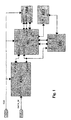
- FIGURE 1 illustrates the arrangement of an SDRAM SDR as storage for correction and track buffering in frontend ICs of optical recording or reproduction devices as for example a DVD-player. Blocks and connections as well as control lines for CD - modes are not included.
- the DVD-player using an SDRAM SDR as storage for correction and track buffering in the frontend IC comprises according to Fig.1a Reed Solomon Decoder RSD, a memory controller MC, a track buffer controller TBC, a backend interface BEI and said SDRAM SDR.
- Reed Solomon Decoder RSD, memory controller MC and said SDRAM SDR are connected to a system clock CLK.
- the Reed Solomon Decoder RSD receives preprocessed data DATA_IN provided from an optical recording medium as for example a DVD.
- the preprocessed data DATA_IN are incoming symbols to the Reed Solomon Decoder RSD as well as not shown ECC-, sector- and frame-start signals from a not shown acquisition part. For the reason of simplification only summarized connections between the unites are shown in Fig.1 which are mostly formed by several lines.
- the Reed Solomon Decoder RSD is connected with said memory controller MC to store and exchange correction data RS_DATA with memory controller MC and provides via a further connection corrected data CR_DATA for said memory controller MC and a track buffer controller TBC which provides via connections track information to_TR and track addresses tr_addr for the memory controller MC.
- Memory controller MC and SDRAM SDR are connected to exchange data via a bus DBUS controlled by addresses addr and RAM control signals ram_ctrl. And the mentioned backend interface BEI receives requested data to_BE from memory controller MC, which have been requested by request commands req, sent to the track buffer controller TBC.
- This block strips off the parity data from incoming preprocessed data DATA_IN and sends it via a memory controller MC to the SDRAM SDR. After the correction data is calculated the faulty data on the SDRAM SDR is exchanged by the corrected data.
- the ECC block stored in the ECC area of the SDRAM SDR is ready for a transfer to the track buffer area.
- the track buffer controller TBC reads sector-wise the corrected data from the ECC area, prepares the validity decision and coordinates the storage of them via a memory control in the track buffer area of the SDRAM SDR.
- the memory controller MC fetches the data sectorwise from the track buffer area of the SDRAM SDR and delivers them to the backend interface BEI.
- This unit has to answer the requests previously described and makes the bookkeeping of the memory resources.
- This unit has to answer the requests previously described and makes the bookkeeping of the memory resources.
- the SDRAM SDR is functionally divided into two areas:
- the ECC - block area must contain at least two ECC blocks because the calculation of the error correction can only be started after the ECC - block is completely read in from the Reed Solomon Decoder RSD.
- the number of inner/outer-runs performed by the Reed Solomon Decoder RSD determines the time when the corrected data CR_DATA is available and can be sent to the memory controller MC. If these processes are finished before the alternate ECC - block is read in only two ECC -blocks need to be stored in the SDRAM SDR; otherwise the number must be increased.
- the track buffer area of the SDRAM SDR which is organized in sectors, can fill the rest of the SDRAM SDR.
- the memory controller MC has to keep the physical addresses of the related processes respecting the size and timing specification of the used SDRAM SDR.
- the data are sent burst wise with a preset burst length to SDRAM SDR and the address for the start of the next burst package is sent to the SDRAM SDR to accelerate the data exchange in the pipeline, the addressing and the data traffic.
- the SDRAM SDR does the incrementation of the address during burst operation internally.
- the SDRAM SDR as shown in Fig. 2 is built around two banks Bank 0 and Bank1 of memory, which are accessed by particularly pipelined address and RAM control signals ram_ctrl.
- DRAMS addressing can be widely done in parallel to the data operation which depends on the locations of the consecutive bursts. This accelerates the speed compared to the common DRAM drastically.
- Most benefit of these features is achieved if the data transfer is done burstwise and if it is organized in the memory so hat the access can be done in ping - pong mode, i.e. changing the bank at each access.
- the system clock CLK synchronizes all transfers although several different data speeds have to be handled.
- FIGS. 3 and 4 show the so called ping-pong operation as used for a SDRAM SDR with 16Mbit Memory setting the so-called CAS - latency to a number of 2 for the used system clock CLK.
- the input-output operations of SDRAM SDR are performed as shown in Fig 3 and 4.
- FIGs 3 and 4 show a first row a illustrating the operations performed on bank Bank 0 and Bank1 of the memory of SDRAM SDR. Each transfer starts by activating the bank denoted by ram_ctrl followed by the read or write command performed by setting the ram_ctrl - signals of figure 1.
- the result of the operation is shown as DIN or DOUT denoting the direction of the data.
- a second row b illustrates system clock CLK
- a third row c shows specific addresses addr which are controlled by memory controller MC. They are split into row - address R0,R1... and column - address Ca, Cb,... sent at the appropriate time.
- a fourth row d illustrates data, which correspondingly occur on bus DBUS. The items are marked with the related locations R. and C. as sent on the address signals addr and an incremented number of the location in the burst.
- the output operation as shown in Fig. 3 demonstrate successive read requests on mutual banks which have addresses and data active at the same time whereas Fig. 4 demonstrates the same for write operation.
Landscapes
- Engineering & Computer Science (AREA)
- Theoretical Computer Science (AREA)
- Signal Processing (AREA)
- Physics & Mathematics (AREA)
- General Engineering & Computer Science (AREA)
- General Physics & Mathematics (AREA)
- Multimedia (AREA)
- Human Computer Interaction (AREA)
- Signal Processing For Digital Recording And Reproducing (AREA)
- Error Detection And Correction (AREA)
- Optical Recording Or Reproduction (AREA)
- Management Or Editing Of Information On Record Carriers (AREA)
- Indexing, Searching, Synchronizing, And The Amount Of Synchronization Travel Of Record Carriers (AREA)
Abstract
Description
The SDRAM is built around two banks of memory, which are accessed by particular pipelined address logic. In contrast to the normal DRAMS addressing can be done in parallel to the data operation and depending on the mode chosen a burst of consecutive locations is operated. This accelerates the speed compared to the common DRAM drastically, on the other hand needs some additional buffering and address control.
SDRAM is an acronym for Synchronous DRAM that means a DRAM technology that uses a clock to synchronize signal input and output on a memory chip. The clock is generated in the driving IC and derived from it's system clock so that the timing of the memory chips and the timing of the driving IC are in synchronization. The data streams for storing, correction and track buffering in frontend ICs of optical recording or reproduction devices are due to several different modes, asynchronous data streams and are not designed in a way that it can be handled directly within an SDRAM because it has no defined burst structure as well as a constant speed as it is commonly used in computer applications. An adaptation of the streams for SDRAM usage is therefore necessary.
In the following sections the mode A is assumed; for the other configurations the data transfer is bypassed the obsolete blocks.
When the sector is finished the track buffer control unit decides if the current sector is valid and increments the location for the next sector or keeps it.
For the backend IC the track buffer control unit handles requests for sending sectors to it verifying that the requested sectors are contained in the trackbuffer area. If they are the request is forwarded to the SDRAM address unit, initializing the backend stream by sending the requested sector address. The backend interface informs the track buffer control unit of the end of the currently received sector.
In the ramless REED - SOLOMON functional configuration the raw data can be sent via the same lines while the correction mask, which is performed by offset and address, may be put to an additional line with a control signal to the backend interface when this data is available. The coordination and format of the stream of data and correction mask is an autonomous task of the backend interface unit.
The SDRAM is functionally divided into two areas:
The rest of the SDRAM can be filled by the track buffer area, which is organized in sectors. The track buffer control unit keeps a cross-reference between a long sector ID and the location in the track buffer area.
To accelerate the data exchange SDRAMs pipeline the addressing and the data traffic:
While the data are received or sent burst wise with a preset length the address for the start of the next burst package can be sent to the SDRAM depending on address and direction of the currently transferred data.
The incrementation of the address during burst operation is done internally by the SDRAM.
The DVD-player using an SDRAM SDR as storage for correction and track buffering in the frontend IC comprises according to Fig.1a Reed Solomon Decoder RSD, a memory controller MC, a track buffer controller TBC, a backend interface BEI and said SDRAM SDR. Reed Solomon Decoder RSD, memory controller MC and said SDRAM SDR are connected to a system clock CLK. The Reed Solomon Decoder RSD receives preprocessed data DATA_IN provided from an optical recording medium as for example a DVD. The preprocessed data DATA_IN are incoming symbols to the Reed Solomon Decoder RSD as well as not shown ECC-, sector- and frame-start signals from a not shown acquisition part. For the reason of simplification only summarized connections between the unites are shown in Fig.1 which are mostly formed by several lines. The Reed Solomon Decoder RSD is connected with said memory controller MC to store and exchange correction data RS_DATA with memory controller MC and provides via a further connection corrected data CR_DATA for said memory controller MC and a track buffer controller TBC which provides via connections track information to_TR and track addresses tr_addr for the memory controller MC. Memory controller MC and SDRAM SDR are connected to exchange data via a bus DBUS controlled by addresses addr and RAM control signals ram_ctrl. And the mentioned backend interface BEI receives requested data to_BE from memory controller MC, which have been requested by request commands req, sent to the track buffer controller TBC.
The SDRAM SDR is functionally divided into two areas:
Most benefit of these features is achieved if the data transfer is done burstwise and if it is organized in the memory so hat the access can be done in ping - pong mode, i.e. changing the bank at each access.
The system clock CLK synchronizes all transfers although several different data speeds have to be handled.
Each of the Figures 3 and 4 show a first row a illustrating the operations performed on
A second row b illustrates system clock CLK, a third row c shows specific addresses addr which are controlled by memory controller MC. They are split into row - address R0,R1... and column - address Ca, Cb,... sent at the appropriate time.
A fourth row d illustrates data, which correspondingly occur on bus DBUS. The items are marked with the related locations R. and C. as sent on the address signals addr and an incremented number of the location in the burst.
The output operation as shown in Fig. 3 demonstrate successive read requests on mutual banks which have addresses and data active at the same time whereas Fig. 4 demonstrates the same for write operation.
Claims (13)
- An optical recording or reproduction apparatus having a track buffer and a track buffer controller for high-speed data transmission, characterised in that an SDRAM (SDR) which is build around two banks of memory which are accessed in a pipelined manner by changing the bank at each access is used as storage for correction and track buffering, and data to be stored in said SDRAM (SDR) or to be read out from said SDRAM (SDR) are organized in bursts by a memory controler (MC) for accelerating the traffic of the SDRAM (SDR).
- Apparatus according to Claim 1 characterised in that the SDRAM (SDR) is coupled to a memory controller (MC) which is furthermore connected with a Reed Solomon Decoder (RSD) and a track buffer controller (TBC) to form a frontend IC of said optical recording or reproduction device.
- Apparatus according to Claim 1 characterised in that the SDRAM (SDR) is coupled to a memory controller (MC) which forms an interface to supervise a data transfer to and from the SDRAM (SDR) and to organize the SDRAM (SDR) burstwise.
- Apparatus according to Claim 1 characterised in that the SDRAM (SDR) accesses randomly symbols from an ECC - block to update it due to correction data (RS_DATA) and to store it back as corrected data (CR_DATA) in a track buffer area of the SDRAM (SDR).
- Apparatus according to Claim 1 characterised in that the SDRAM (SDR) stores raw data coming from a Reed Solomon Decoder (RSD) into the SDRAM (SDR) by help of system clock CLK while the Reed Solomon Decoder (RSD) performs a second and further following inner/outer correction after the data was delivered by the Reed Solomon Decoder (RSD) and depending on how and when the Reed Solomon Decoder (RSD) makes this data available the SDRAM (SDR) accesses randomly symbols from the ECC - block to update it due to the correction data (RS_DATA) and to store it back as corrected data (CR_DATA) in a track buffer area of the SDRAM (SDR).
- Apparatus according to Claim 2 characterised in that said front end IC performs bitwise descrambling and EDC calculation of data.
- Apparatus according to Claim 1 characterised in that the SDRAM (SDR) in a case if a CD is reproduced by the optical recording or reproduction apparatus raw data coming from a Reed Solomon Decoder (RSD) are stored into the SDRAM (SDR) by help of a system clock (CLK) and are stored to SDRAM (SDR) under supervision of a track buffer controler (TBC) according to the CD nessities.
- Apparatus according to Claim 7 characterised in that raw data are stored from the Reed Solomon Decoder (RSD) via memory controller (MC) to perform the correction.
- Apparatus according to Claim 1 characterised in that the SDRAM (SDR) is used in a case if a DVD is reproduced by the optical recording or reproduction apparatus raw data coming from a Reed Solomon Decoder (RSD) are stored into the SDRAM (SDR) by help of a system clock (CLK) while the Reed Solomon Decoder (RSD) performs inner/outer corrections in the SDRAM (SDR) after the data was delivered by the Reed Solomon Decoder (RSD), and the corrected data are modified and restored under supervision of a track buffer controller (TBC) according to the DVD - necessities.
- Apparatus according to Claim 1 characterised in that the part of the SDRAM (SDR) used to store data for correction forms an area of the SDRAM (SDR) which contains at least two ECC blocks.
- Apparatus according to Claim 1 characterised in that the SDRAM (SDR) receives and sends data burst wise with a preset length and an address for a start of a next burst package is sent to the SDRAM (SDR) depending on address and direction of currently transferred data.
- A method of using an SDRAM (SDR) as storage for correction and track buffering of data in frontend ICs of optical recording or reproduction devices, comprising the step of:organizing data to be stored or read by the SDRAM (SDR) in predetermined bursts to perform a mode of data access to accelerate the speed for correction and track buffering of data within the SDRAM (SDR) of frontend ICs of optical recording or reproduction devices by the usage of an SDRAM (SDR) which is build around two banks of memory which are accessed in a pipelined manner by changing the bank at each access.
- A method according to Claim 12 characterised in that said bursts are performed within a memory controller (MC) controlling the SDRAM (SDR) as storage for correction and track buffering of data.
Priority Applications (2)
| Application Number | Priority Date | Filing Date | Title |
|---|---|---|---|
| DK00985157T DK1245027T3 (en) | 1999-12-17 | 2000-12-12 | Use of an SDRAM as storage for correction and trace intermediate storage in front end IDs for optical recording or reproducing devices |
| EP00985157A EP1245027B1 (en) | 1999-12-17 | 2000-12-12 | USAGE OF AN SDRAM AS STORAGE FOR CORRECTION AND TRACK BUFFERING IN FRONTEND ICs OF OPTICAL RECORDING OR REPRODUCTION DEVICES |
Applications Claiming Priority (4)
| Application Number | Priority Date | Filing Date | Title |
|---|---|---|---|
| EP99125206 | 1999-12-17 | ||
| EP99125206 | 1999-12-17 | ||
| PCT/EP2000/012551 WO2001045101A2 (en) | 1999-12-17 | 2000-12-12 | USAGE OF AN SDRAM AS STORAGE FOR CORRECTION AND TRACK BUFFERING IN FRONTEND ICs OF OPTICAL RECORDING OR REPRODUCTION DEVICES |
| EP00985157A EP1245027B1 (en) | 1999-12-17 | 2000-12-12 | USAGE OF AN SDRAM AS STORAGE FOR CORRECTION AND TRACK BUFFERING IN FRONTEND ICs OF OPTICAL RECORDING OR REPRODUCTION DEVICES |
Publications (2)
| Publication Number | Publication Date |
|---|---|
| EP1245027A2 EP1245027A2 (en) | 2002-10-02 |
| EP1245027B1 true EP1245027B1 (en) | 2004-09-15 |
Family
ID=8239645
Family Applications (1)
| Application Number | Title | Priority Date | Filing Date |
|---|---|---|---|
| EP00985157A Expired - Lifetime EP1245027B1 (en) | 1999-12-17 | 2000-12-12 | USAGE OF AN SDRAM AS STORAGE FOR CORRECTION AND TRACK BUFFERING IN FRONTEND ICs OF OPTICAL RECORDING OR REPRODUCTION DEVICES |
Country Status (14)
| Country | Link |
|---|---|
| US (1) | US7346830B2 (en) |
| EP (1) | EP1245027B1 (en) |
| JP (1) | JP2003517173A (en) |
| KR (1) | KR100751475B1 (en) |
| CN (1) | CN1218314C (en) |
| AT (1) | ATE276572T1 (en) |
| AU (1) | AU776026B2 (en) |
| DE (1) | DE60013904T2 (en) |
| DK (1) | DK1245027T3 (en) |
| ES (1) | ES2228645T3 (en) |
| MX (1) | MXPA02005837A (en) |
| PL (1) | PL356023A1 (en) |
| PT (1) | PT1245027E (en) |
| WO (1) | WO2001045101A2 (en) |
Families Citing this family (8)
| Publication number | Priority date | Publication date | Assignee | Title |
|---|---|---|---|---|
| US7395488B2 (en) * | 2004-12-29 | 2008-07-01 | Zoran Corporation | System and method for efficient use of memory device bandwidth |
| US8074153B2 (en) * | 2005-12-12 | 2011-12-06 | Mediatek Inc. | Error correction devices and correction methods |
| US7802169B2 (en) * | 2005-12-12 | 2010-09-21 | Mediatek Inc. | Error correction devices and correction methods |
| TWM299458U (en) * | 2006-04-21 | 2006-10-11 | Taiwan Microloops Corp | Heat spreader with composite micro-structure |
| US7689894B2 (en) * | 2006-05-11 | 2010-03-30 | Mediatek Inc. | Decoding apparatus and method therefor |
| US7916866B2 (en) * | 2006-05-19 | 2011-03-29 | Mediatek, Inc. | Apparatus for descrambling a data retrieved from an optical storage medium, and method therefor |
| KR20080036838A (en) * | 2006-10-24 | 2008-04-29 | 삼성전자주식회사 | Error correction method of optical information storage media playback / recording device |
| US10509577B2 (en) * | 2014-06-05 | 2019-12-17 | Pure Storage, Inc. | Reliable storage in a dispersed storage network |
Family Cites Families (20)
| Publication number | Priority date | Publication date | Assignee | Title |
|---|---|---|---|---|
| GB2276255A (en) | 1993-02-17 | 1994-09-21 | Andor Int Ltd | Track buffer with embedded error data |
| JP3284900B2 (en) * | 1996-10-18 | 2002-05-20 | 松下電器産業株式会社 | Data decryption method |
| US5974514A (en) * | 1996-11-12 | 1999-10-26 | Hewlett-Packard | Controlling SDRAM memory by using truncated burst read-modify-write memory operations |
| KR100217181B1 (en) | 1997-01-21 | 1999-09-01 | 윤종용 | System Decoder and Track Buffering Control Method for High-Speed Data Transmission |
| KR100233722B1 (en) * | 1997-02-20 | 1999-12-01 | 윤종용 | Apparatus for testing a digital signal process part of digital video disk player |
| JP3834922B2 (en) * | 1997-04-08 | 2006-10-18 | ソニー株式会社 | Error correction apparatus and method |
| US6278645B1 (en) * | 1997-04-11 | 2001-08-21 | 3Dlabs Inc., Ltd. | High speed video frame buffer |
| US5896346A (en) * | 1997-08-21 | 1999-04-20 | International Business Machines Corporation | High speed and low cost SDRAM memory subsystem |
| JPH1186464A (en) * | 1997-09-05 | 1999-03-30 | Victor Co Of Japan Ltd | Signal processor |
| JPH1198462A (en) * | 1997-09-19 | 1999-04-09 | Hitachi Ltd | Data playback device |
| JPH11110919A (en) * | 1997-09-30 | 1999-04-23 | Victor Co Of Japan Ltd | Digital signal recording system and recording medium |
| EP0917143B1 (en) | 1997-11-11 | 2004-01-02 | Deutsche Thomson-Brandt Gmbh | Method and apparatus for controlling the buffering of a data stream |
| JP3307579B2 (en) * | 1998-01-28 | 2002-07-24 | インターナショナル・ビジネス・マシーンズ・コーポレーション | Data storage system |
| US6587896B1 (en) * | 1998-02-27 | 2003-07-01 | Micron Technology, Inc. | Impedance matching device for high speed memory bus |
| CN100447882C (en) * | 1998-05-06 | 2008-12-31 | 汤姆森特许公司 | Replay Bitstream Processing |
| JPH11328677A (en) * | 1998-05-20 | 1999-11-30 | Sony Corp | Playback device |
| US6272153B1 (en) * | 1998-06-26 | 2001-08-07 | Lsi Logic Corporation | DVD audio decoder having a central sync-controller architecture |
| US6330626B1 (en) * | 1999-05-05 | 2001-12-11 | Qlogic Corporation | Systems and methods for a disk controller memory architecture |
| US6754858B2 (en) * | 2001-03-29 | 2004-06-22 | International Business Machines Corporation | SDRAM address error detection method and apparatus |
| US6868519B2 (en) * | 2001-04-23 | 2005-03-15 | Lucent Technologies Inc. | Reducing scintillation effects for optical free-space transmission |
-
2000
- 2000-12-12 DK DK00985157T patent/DK1245027T3/en active
- 2000-12-12 KR KR1020027006767A patent/KR100751475B1/en not_active Expired - Fee Related
- 2000-12-12 AT AT00985157T patent/ATE276572T1/en active
- 2000-12-12 JP JP2001545309A patent/JP2003517173A/en active Pending
- 2000-12-12 WO PCT/EP2000/012551 patent/WO2001045101A2/en not_active Ceased
- 2000-12-12 PL PL00356023A patent/PL356023A1/en unknown
- 2000-12-12 US US10/168,161 patent/US7346830B2/en not_active Expired - Fee Related
- 2000-12-12 EP EP00985157A patent/EP1245027B1/en not_active Expired - Lifetime
- 2000-12-12 DE DE60013904T patent/DE60013904T2/en not_active Expired - Lifetime
- 2000-12-12 AU AU21663/01A patent/AU776026B2/en not_active Ceased
- 2000-12-12 MX MXPA02005837A patent/MXPA02005837A/en active IP Right Grant
- 2000-12-12 ES ES00985157T patent/ES2228645T3/en not_active Expired - Lifetime
- 2000-12-12 PT PT00985157T patent/PT1245027E/en unknown
- 2000-12-12 CN CN008171734A patent/CN1218314C/en not_active Expired - Fee Related
Also Published As
| Publication number | Publication date |
|---|---|
| DE60013904T2 (en) | 2005-09-29 |
| CN1218314C (en) | 2005-09-07 |
| DE60013904D1 (en) | 2004-10-21 |
| PL356023A1 (en) | 2004-05-31 |
| ATE276572T1 (en) | 2004-10-15 |
| KR20020059799A (en) | 2002-07-13 |
| EP1245027A2 (en) | 2002-10-02 |
| CN1409856A (en) | 2003-04-09 |
| AU2166301A (en) | 2001-06-25 |
| JP2003517173A (en) | 2003-05-20 |
| US7346830B2 (en) | 2008-03-18 |
| WO2001045101A2 (en) | 2001-06-21 |
| DK1245027T3 (en) | 2004-11-15 |
| US20020191967A1 (en) | 2002-12-19 |
| WO2001045101A3 (en) | 2001-11-08 |
| KR100751475B1 (en) | 2007-08-23 |
| MXPA02005837A (en) | 2005-07-01 |
| PT1245027E (en) | 2005-01-31 |
| ES2228645T3 (en) | 2005-04-16 |
| AU776026B2 (en) | 2004-08-26 |
Similar Documents
| Publication | Publication Date | Title |
|---|---|---|
| KR100385370B1 (en) | Improved memory system apparatus and method | |
| KR20010080966A (en) | Signal processor for correcting and detecting errors | |
| US5687393A (en) | System for controlling responses to requests over a data bus between a plurality of master controllers and a slave storage controller by inserting control characters | |
| US7346830B2 (en) | Usage of an SDRAM as storage for correction and track buffering in frontend ICs of optical recording or reproduction devices | |
| US4841513A (en) | Sequential buffer device | |
| KR100653569B1 (en) | Data transmission device, data transmission system, and data transmission method using double buffering | |
| US5768502A (en) | Error correcting apparatus for detecting and correcting errors in data accessed from a storage medium | |
| JPH1198462A (en) | Data playback device | |
| KR100276407B1 (en) | Dynamic altering band-width data transferring method and the system | |
| JP2006268814A (en) | Optical storage system comprising interface for transferring data | |
| US6728806B2 (en) | Data processing unit | |
| KR100189530B1 (en) | Data interface method between microprocessor and memory | |
| US6499082B1 (en) | Method of transferring data from large capacity data storage device | |
| US6697921B1 (en) | Signal processor providing an increased memory access rate | |
| JP4707351B2 (en) | Multi-bank memory scheduling method | |
| US7103707B2 (en) | Access control unit and method for use with synchronous dynamic random access memory device | |
| KR100189529B1 (en) | Memory control apparatus and method of disk data decoder for DVD | |
| US20060184858A1 (en) | Memory circuit, such as a DRAM, comprising an error correcting mechanism | |
| KR100234391B1 (en) | ECC memory control apparatus of digital video disk | |
| JP2570986B2 (en) | Data transfer control device and method | |
| KR19990016581A (en) | Sector Decode and Atapi Devices with Integrated Memory | |
| JP2002091823A (en) | Memory controller to be used for image display device | |
| JP3561502B2 (en) | Improved memory system and method | |
| JPH08179894A (en) | Memory system and memory system applied to disk recording / reproducing apparatus | |
| JPH1185672A (en) | Data transmission equipment |
Legal Events
| Date | Code | Title | Description |
|---|---|---|---|
| PUAI | Public reference made under article 153(3) epc to a published international application that has entered the european phase |
Free format text: ORIGINAL CODE: 0009012 |
|
| 17P | Request for examination filed |
Effective date: 20020604 |
|
| AK | Designated contracting states |
Kind code of ref document: A2 Designated state(s): AT BE CH CY DE DK ES FI FR GB GR IE IT LI LU MC NL PT SE TR |
|
| AX | Request for extension of the european patent |
Free format text: AL;LT;LV;MK;RO;SI |
|
| 17Q | First examination report despatched |
Effective date: 20021106 |
|
| GRAP | Despatch of communication of intention to grant a patent |
Free format text: ORIGINAL CODE: EPIDOSNIGR1 |
|
| RAP1 | Party data changed (applicant data changed or rights of an application transferred) |
Owner name: THOMSON LICENSING S.A. |
|
| RIN1 | Information on inventor provided before grant (corrected) |
Inventor name: RUTSCHMANN, RICHARD Inventor name: KABUTZ, MARTEN Inventor name: FREISSMANN, LOTHAR |
|
| GRAS | Grant fee paid |
Free format text: ORIGINAL CODE: EPIDOSNIGR3 |
|
| GRAA | (expected) grant |
Free format text: ORIGINAL CODE: 0009210 |
|
| AK | Designated contracting states |
Kind code of ref document: B1 Designated state(s): AT BE CH CY DE DK ES FI FR GB GR IE IT LI LU MC NL PT SE TR |
|
| PG25 | Lapsed in a contracting state [announced via postgrant information from national office to epo] |
Ref country code: CY Free format text: LAPSE BECAUSE OF FAILURE TO SUBMIT A TRANSLATION OF THE DESCRIPTION OR TO PAY THE FEE WITHIN THE PRESCRIBED TIME-LIMIT Effective date: 20040915 |
|
| REG | Reference to a national code |
Ref country code: GB Ref legal event code: FG4D Ref country code: CH Ref legal event code: EP |
|
| REG | Reference to a national code |
Ref country code: IE Ref legal event code: FG4D Ref country code: GB Ref legal event code: 746 Effective date: 20040929 |
|
| REF | Corresponds to: |
Ref document number: 60013904 Country of ref document: DE Date of ref document: 20041021 Kind code of ref document: P |
|
| REG | Reference to a national code |
Ref country code: DK Ref legal event code: T3 Ref country code: CH Ref legal event code: NV Representative=s name: KIRKER & CIE SA |
|
| PG25 | Lapsed in a contracting state [announced via postgrant information from national office to epo] |
Ref country code: LU Free format text: LAPSE BECAUSE OF NON-PAYMENT OF DUE FEES Effective date: 20041212 |
|
| PG25 | Lapsed in a contracting state [announced via postgrant information from national office to epo] |
Ref country code: IE Free format text: LAPSE BECAUSE OF NON-PAYMENT OF DUE FEES Effective date: 20041213 |
|
| PG25 | Lapsed in a contracting state [announced via postgrant information from national office to epo] |
Ref country code: GR Free format text: LAPSE BECAUSE OF FAILURE TO SUBMIT A TRANSLATION OF THE DESCRIPTION OR TO PAY THE FEE WITHIN THE PRESCRIBED TIME-LIMIT Effective date: 20041215 |
|
| REG | Reference to a national code |
Ref country code: SE Ref legal event code: TRGR |
|
| PG25 | Lapsed in a contracting state [announced via postgrant information from national office to epo] |
Ref country code: MC Free format text: LAPSE BECAUSE OF NON-PAYMENT OF DUE FEES Effective date: 20041231 |
|
| REG | Reference to a national code |
Ref country code: PT Ref legal event code: SC4A Effective date: 20041203 |
|
| LTIE | Lt: invalidation of european patent or patent extension |
Effective date: 20040915 |
|
| REG | Reference to a national code |
Ref country code: ES Ref legal event code: FG2A Ref document number: 2228645 Country of ref document: ES Kind code of ref document: T3 |
|
| PLBE | No opposition filed within time limit |
Free format text: ORIGINAL CODE: 0009261 |
|
| STAA | Information on the status of an ep patent application or granted ep patent |
Free format text: STATUS: NO OPPOSITION FILED WITHIN TIME LIMIT |
|
| ET | Fr: translation filed | ||
| 26N | No opposition filed |
Effective date: 20050616 |
|
| REG | Reference to a national code |
Ref country code: IE Ref legal event code: MM4A |
|
| REG | Reference to a national code |
Ref country code: FR Ref legal event code: D6 |
|
| REG | Reference to a national code |
Ref country code: FR Ref legal event code: PLFP Year of fee payment: 16 |
|
| PGFP | Annual fee paid to national office [announced via postgrant information from national office to epo] |
Ref country code: GB Payment date: 20151215 Year of fee payment: 16 Ref country code: DE Payment date: 20151215 Year of fee payment: 16 |
|
| PGFP | Annual fee paid to national office [announced via postgrant information from national office to epo] |
Ref country code: FR Payment date: 20151222 Year of fee payment: 16 |
|
| PGFP | Annual fee paid to national office [announced via postgrant information from national office to epo] |
Ref country code: NL Payment date: 20161212 Year of fee payment: 17 Ref country code: DK Payment date: 20161212 Year of fee payment: 17 Ref country code: FI Payment date: 20161212 Year of fee payment: 17 Ref country code: CH Payment date: 20161213 Year of fee payment: 17 |
|
| PGFP | Annual fee paid to national office [announced via postgrant information from national office to epo] |
Ref country code: BE Payment date: 20161114 Year of fee payment: 17 Ref country code: ES Payment date: 20161111 Year of fee payment: 17 Ref country code: IT Payment date: 20161221 Year of fee payment: 17 Ref country code: PT Payment date: 20161212 Year of fee payment: 17 Ref country code: SE Payment date: 20161213 Year of fee payment: 17 Ref country code: AT Payment date: 20161125 Year of fee payment: 17 |
|
| PGFP | Annual fee paid to national office [announced via postgrant information from national office to epo] |
Ref country code: TR Payment date: 20161124 Year of fee payment: 17 |
|
| REG | Reference to a national code |
Ref country code: DE Ref legal event code: R119 Ref document number: 60013904 Country of ref document: DE |
|
| GBPC | Gb: european patent ceased through non-payment of renewal fee |
Effective date: 20161212 |
|
| REG | Reference to a national code |
Ref country code: FR Ref legal event code: ST Effective date: 20170831 |
|
| PG25 | Lapsed in a contracting state [announced via postgrant information from national office to epo] |
Ref country code: FR Free format text: LAPSE BECAUSE OF NON-PAYMENT OF DUE FEES Effective date: 20170102 |
|
| PG25 | Lapsed in a contracting state [announced via postgrant information from national office to epo] |
Ref country code: GB Free format text: LAPSE BECAUSE OF NON-PAYMENT OF DUE FEES Effective date: 20161212 Ref country code: DE Free format text: LAPSE BECAUSE OF NON-PAYMENT OF DUE FEES Effective date: 20170701 |
|
| REG | Reference to a national code |
Ref country code: DK Ref legal event code: EBP Effective date: 20171231 |
|
| PG25 | Lapsed in a contracting state [announced via postgrant information from national office to epo] |
Ref country code: FI Free format text: LAPSE BECAUSE OF NON-PAYMENT OF DUE FEES Effective date: 20171212 Ref country code: PT Free format text: LAPSE BECAUSE OF NON-PAYMENT OF DUE FEES Effective date: 20180612 |
|
| REG | Reference to a national code |
Ref country code: CH Ref legal event code: PL |
|
| REG | Reference to a national code |
Ref country code: NL Ref legal event code: MM Effective date: 20180101 |
|
| REG | Reference to a national code |
Ref country code: AT Ref legal event code: MM01 Ref document number: 276572 Country of ref document: AT Kind code of ref document: T Effective date: 20171212 |
|
| PG25 | Lapsed in a contracting state [announced via postgrant information from national office to epo] |
Ref country code: SE Free format text: LAPSE BECAUSE OF NON-PAYMENT OF DUE FEES Effective date: 20171213 |
|
| PG25 | Lapsed in a contracting state [announced via postgrant information from national office to epo] |
Ref country code: NL Free format text: LAPSE BECAUSE OF NON-PAYMENT OF DUE FEES Effective date: 20180101 |
|
| REG | Reference to a national code |
Ref country code: BE Ref legal event code: MM Effective date: 20171231 |
|
| PG25 | Lapsed in a contracting state [announced via postgrant information from national office to epo] |
Ref country code: IT Free format text: LAPSE BECAUSE OF NON-PAYMENT OF DUE FEES Effective date: 20171212 |
|
| PG25 | Lapsed in a contracting state [announced via postgrant information from national office to epo] |
Ref country code: BE Free format text: LAPSE BECAUSE OF NON-PAYMENT OF DUE FEES Effective date: 20171231 Ref country code: CH Free format text: LAPSE BECAUSE OF NON-PAYMENT OF DUE FEES Effective date: 20171231 Ref country code: AT Free format text: LAPSE BECAUSE OF NON-PAYMENT OF DUE FEES Effective date: 20171212 Ref country code: LI Free format text: LAPSE BECAUSE OF NON-PAYMENT OF DUE FEES Effective date: 20171231 |
|
| PG25 | Lapsed in a contracting state [announced via postgrant information from national office to epo] |
Ref country code: DK Free format text: LAPSE BECAUSE OF NON-PAYMENT OF DUE FEES Effective date: 20171231 |
|
| REG | Reference to a national code |
Ref country code: ES Ref legal event code: FD2A Effective date: 20190702 |
|
| PG25 | Lapsed in a contracting state [announced via postgrant information from national office to epo] |
Ref country code: ES Free format text: LAPSE BECAUSE OF NON-PAYMENT OF DUE FEES Effective date: 20171213 |
|
| PG25 | Lapsed in a contracting state [announced via postgrant information from national office to epo] |
Ref country code: TR Free format text: LAPSE BECAUSE OF NON-PAYMENT OF DUE FEES Effective date: 20171212 |