EP1244220A2 - Method for modulating digital data and apparatus therefor - Google Patents
Method for modulating digital data and apparatus therefor Download PDFInfo
- Publication number
- EP1244220A2 EP1244220A2 EP01122737A EP01122737A EP1244220A2 EP 1244220 A2 EP1244220 A2 EP 1244220A2 EP 01122737 A EP01122737 A EP 01122737A EP 01122737 A EP01122737 A EP 01122737A EP 1244220 A2 EP1244220 A2 EP 1244220A2
- Authority
- EP
- European Patent Office
- Prior art keywords
- digital data
- data stream
- dsv
- penalty
- value
- Prior art date
- Legal status (The legal status is an assumption and is not a legal conclusion. Google has not performed a legal analysis and makes no representation as to the accuracy of the status listed.)
- Granted
Links
Images



Classifications
-
- H—ELECTRICITY
- H03—ELECTRONIC CIRCUITRY
- H03M—CODING; DECODING; CODE CONVERSION IN GENERAL
- H03M7/00—Conversion of a code where information is represented by a given sequence or number of digits to a code where the same, similar or subset of information is represented by a different sequence or number of digits
- H03M7/30—Compression; Expansion; Suppression of unnecessary data, e.g. redundancy reduction
- H03M7/46—Conversion to or from run-length codes, i.e. by representing the number of consecutive digits, or groups of digits, of the same kind by a code word and a digit indicative of that kind
-
- H—ELECTRICITY
- H03—ELECTRONIC CIRCUITRY
- H03M—CODING; DECODING; CODE CONVERSION IN GENERAL
- H03M5/00—Conversion of the form of the representation of individual digits
- H03M5/02—Conversion to or from representation by pulses
- H03M5/04—Conversion to or from representation by pulses the pulses having two levels
- H03M5/14—Code representation, e.g. transition, for a given bit cell depending on the information in one or more adjacent bit cells, e.g. delay modulation code, double density code
- H03M5/145—Conversion to or from block codes or representations thereof
Definitions
- the present invention relates to a method for modulating digital data and apparatus therefor and particularly, to a method for modulating digital data and apparatus therefor which determines digital data stream coded by Run Length Limited (hereinafter as RLL) swiftly and precisely so as to record data in a record medium.
- RLL Run Length Limited
- Non-return-to-Zero-Inverse (hereinafter NRZI) code shows that no change is in magnetic flux of a record medium if the signal detected in the record medium is a binary number '0' and that the direction of magnetic flux recorded in the record medium is reversed if the signal detected in the record medium is a binary number '1' thus to record data in the record medium and detects or regenerate the recorded signal.
- NRZI Non-return-to-Zero-Inverse
- RLL Run Length Limited
- the first restriction condition is that among bits having consecutive 1, at least a bit having 'o' value bit should exist. For instance, a data bit becomes three times as large as a data record density stored without a specific condition and accordingly, the data is recorded in the record medium with a high record density. At this time, on the first restriction condition, the data recorded in the record medium should be positioned in the distance that magnetic flux polarity of the data bit can be sorted even though the data is recorded in the record medium with a high record density.
- the first restriction condition is that bits having a certain '0' bit value in the record medium are recorded and symbols do not intervene each other when the recorded data is regenerated.
- the second restriction condition is that the numbers of bits having 0 value bits should not many among the bits having consecutive 1 value bits. If the bits which have 0 value are not spread but is formed in a stream, the clock which generates a phase lock circuit is not motivated. Therefore, clock signals can be restored from the regenerated data by locking the phase lock circuit in the position where transition of the regenerated data is performed.
- the data stream modulated satisfying the restriction conditions generally includes DC component. If the data stream in which the DC component is not removed is recorded in the record medium, when the data stream is regenerated, error signals such as tracking errors of the record medium are generated and accordingly, normal output of regeneration data can not be performed. Namely, the DC composition signals interrupt the recorded digital signals from dealing with low frequency components normally. By removing the low frequency components, consecutive tracking controlling is enabled and accordingly when the data recorded in the record medium is detected through the optical recording carrier, the recorded data can be normally regenerated. Therefore, if the low frequency components are controlled properly, tracking controlling of the record medium is capable of not being influenced on the low frequency components.
- the Digital Sum Value (hereinafter as DSV) of modulated data stream controlling technique is developed.
- the DSV for example, in case of using NRZI modulating method, is obtained by modulating the m units of source words into n units of channel words and adding up the channel words.
- the NRZI modulating method allocate a binary number '0' bit of the channel words to -1 value and a binary number '1' bit is allocated to a '+1' value. Therefore, a digital data stream having a small DSV becomes a digital data stream containing small amount of DC component.
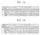
- Figure 1a and Figure 1b are tables showing the first and second digital data stream to describe the method how to determine digital data stream according to the conventional art and the table includes a bipolar code stream obtained from each bit of the first and second digital data stream, the DSV obtained from the bipolar code stream and an absolute value of the DSV and the squared value of the DVS obtained from the DVS.
- the second digital data stream is determined as a code word since the small DSV of the second digital data stream is fit to the data stream condition having a small DC component.
- the absolute value of the DSV of the first digital data stream is 50 1+0+1+0+,+2+3+4)
- the absolute value of the DSV of the second digital data stream is 39 (1+0+1+0,+0+1+0). Accordingly, the second digital data stream is determined as a code word since the small DSV of the second digital data stream fits the data stream condition having a small DC component.
- the squared value of the DSV of the first digital data stream is 118 (1+0+1+0+4+9+16)
- the squared value of the DSV of the second digital data stream is 92 (1+0+1+0,+0+1+0). Accordingly, the second digital data stream is determined as a code word since the small DSV of the second digital data stream fits the data stream condition having a small DC component.
- Figure 2a and Figure 2b are graphs showing each size of the DSV of the Figure 1a and Figure 1b according to the conventional art.
- the number of the DSV having bigger value than the level of M
- 2 as shown in Figure 2a, for the first digital data stream is 15 times, and for the second digital data stream is 12. Therefore, the second digital data stream having a small number of the DSV which are larger than a certain critical level is determined as a code word.
- the conventional modulating method for a digital data stream determines by using the DSV calculated in terms of bit, absolute value of the DSV and the squared value of the DSV.
- the digital data stream is determined by using the calculated value in terms of bite or word.
- the conventional data modulating methods described above has a disadvantage that the circuit is large and accordingly, the composition of the hardware is very complicated and the efficiency is not good compared to the size of the circuit since many multipliers are necessary to select the second digital data stream when it is realized in the form of hardware.
- the object of the present invention is to provide a method for modulating digital data and apparatus therefor for determining the digital data stream having the minimum DSV swiftly and precisely.
- Another object of the present invention is to provide a method for modulating digital data and apparatus therefor for determining the digital data stream having the minimum DSV using weight values corresponding to the DSV and preset critical value swiftly and precisely.
- the digital data modulating method in accordance with the present invention includes the steps of: comparing a preset critical value and DSV of a certain digital data stream; computing the penalty of the digital data stream by multiplying the number of the time that the DSV of the digital data stream is larger than the critical value by a preset weight value of the critical value; and comparing the penalty of the digital data and a penalty of another digital data stream and determining a digital data stream with a smaller penalty for the digital data stream.
- the apparatus for modulating digital data includes: a DSV calculating unit for computing DSV of the inputted digital data; a DSV lever detector for outputting the weight value corresponding to the critical values comparing the DSV and the preset critical value; and a penalty generating unit for generating a penalty of the digital data stream using the DSV detected by the level detector.
- Figure 3 is a block diagram showing an apparatus for modulating digital data stream in accordance with the present invention and the apparatus for modulating digital data includes: a DSV calculating unit 1 for computing DSV of the inputted digital data; a plurality of level detectors 2-1, 2-2,..., and 2-n for outputting the weight value corresponding to the DSV; a weight value switching unit 3 for outputting only the weight values detected by the level detectors 2-1, 2-2,...,and 2-n ; a weight value adder 4 for adding the outputted weight values; and a penalty generating unit 5 for generating a penalty of the digital data stream using the added weight value and the data block flag.
- a DSV calculating unit 1 for computing DSV of the inputted digital data
- a plurality of level detectors 2-1, 2-2,..., and 2-n for outputting the weight value corresponding to the DSV
- a weight value switching unit 3 for outputting only the weight values detected by the level detectors 2-1, 2-2,...,and 2-n
- FIG. 4 is a flow chart showing the method for modulating digital data stream in accordance with the present invention.
- the first step ST1 is to receive a digital data stream. For example, after executing a Non-Return-to-Zero-Inverse(NRZI) coding, a DSV of the coded digital data stream is calculated.
- the second step ST2 is, for example, to perform NRZI coding and then compute the DSV of the coded digital data stream.
- the third step ST3 is to determine weight values from the critical values of a number of preset levels corresponding to the computed DSV.
- the fourth step ST4 is to compute the penalty by multiplying the weight value by the levels.
- the fifth step ST5 and sixth step ST6 are to select and output a digital data stream having smaller penalty by comparing different digital data streams from the above described digital data stream. The method for selecting the digital data stream will be described here in detail.
- Figures 5a and 5b are tables showing the first and second digital data stream for describing method for modulating digital data stream in accordance with the present invention and it contains bipolar code streams from the first and second digital data streams and the DSV obtained from the bipolar code streams.
- Figures 6a and 6b are graphs showing the size of the DSV of a pair of critical values in Figures 5a and 5b according to the present invention and the DSV of the digital data stream corresponding to the pair of critical levels M1 and M2 set centering around the DSV of '0' is marked in the graph.
- weight value of '0' is allocated to DSV smaller than the absolute value of the critical value(for example, 2)
- weight value of '0' is allocated and to larger DSV
- weight value of '2' is allocated. Accordingly, a digital data stream having smaller DSV among a plurality of digital data streams is determined precisely and swiftly by imposing penalty to the bits out of the critical value level. Therefore, the penalty P of a digital data stream, as shown in following equation 1, is obtained precisely and swiftly by adding weight values of the bits out of the critical value level.
- V i indicates the number of data larger than the critical value and W i indicates the correspond weight value.
- the penalty of the first digital data stream is 28 since V i is 14. Also, the penalty of the second digital data stream is 22 since V i is 11. Therefore, the first digital data having a smaller DSV stream is selected.
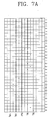
- Figures 7a and 7b are graphs showing the size of DSV of a plurality of critical values in Figures 5a and 5b according to the present invention and the DSV of the digital data stream according to the multiple critical value levels M1, M2, ..., -M2, ... centering around the DSV of '0' is indicated in the graph.
- values such as 0, 1, 2,... can be allocated to the weight values W1, W2,... of the critical values. Therefore, the penalty P of the digital data stream having a value out of the DSV of '0' is obtained by the equation 2.
- V th-i indicates the number of data which is larger than the critical value of V th
- W th-i is the weight value allotted to the critical value of V th .
- the second digital data stream is selected as a code word since the penalty P of the digital data stream divides the size of the DSV of the digital data stream precisely.
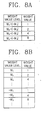
- Figure 8a is a table showing a case in which each pair of weight values allocated to a plurality of critical values centering around the DSV of '0' have same value symmetrically.
- Figure 8b is a table showing the case in which the weight values allocated to upper critical values and those of lower critical values centering around the DSV of '0' are different each other.
- digital data stream is determined using the DSV computed in bits.
- digital data stream is determined using the DSV calculated in bites or words actually.
- weight values corresponding to the levels are allocated to the multiplier of 2, but other multipliers can be allocated.
- the DSV calculating unit additionally includes an absolute value processing unit since it uses absolute values in case that the levels of DSV are set symmetrically.
- the method for modulating a digital data stream can be applied to EFM plus and guided scrambling methods.
- the method for modulating digital data and apparatus therefor in accordance with the present invention can select digital data stream which will be modulated among a number of digital data streams precisely and swiftly by obtaining penalty using the DSV and corresponding weight value among inputted digital data stream and also it can reduce complexity of hardware.
Landscapes
- Engineering & Computer Science (AREA)
- Theoretical Computer Science (AREA)
- Signal Processing For Digital Recording And Reproducing (AREA)
Abstract
Description


Claims (14)
- A digital data modulating method comprising the steps of:comparing a preset critical value and DSV of a certain digital data stream;computing the penalty of the digital data stream by multiplying the number of the time that the DSV of the digital data stream is larger than the critical value by a preset weight value corresponding to the critical value; andcomparing the penalty of the digital data stream and a penalty of another digital data stream to determine a digital data stream with a smaller penalty.
- The method of claim 1, wherein said preset critical values are plural.
- The method of claim 1 or 2, wherein a different weight value is allocated to each of the critical values.
- The method of at least one of the preceding claims, wherein the weight value increases in proportion to an increase in the critical values.
- The method of at least one of the preceding claims, wherein the weight value increases by a multiplier of 2 corresponding to the critical values.
- The method of at least one of the preceding claims, wherein the preset critical values have a different polarity.
- The method of at least one of the preceding claims, wherein the step of comparing the DSV is performed in terms of bit or byte or word included in the digital data stream.
- The method of at least one of the preceding claims, wherein the number of the critical values is two; and
the penalty is obtained by an equation ofof which Vi indicates the number of data which is larger than the critical value, and Wi indicates a weight value thereof.
- The method of at least one of claims 1 to 7, wherein the number of the critical values is larger than two; and
the penalty is obtained by an equation ofof which Vth-i indicates the number of data which is larger than the critical value, and Wth-i indicates a weight value allotted thereto.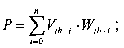
- The method of at least one of the preceding claims, wherein the preset critical values have different absolute values and different polarities.
- The method of at least one of the preceding claims, wherein the preset critical values are set as pairs each having same absolute values and different polarities.
- A digital data modulating apparatus comprising:a DSV computing unit for computing a DSV of an inputted digital data;a DSV level detector for comparing the DSV and a preset critical value and outputting a weight value corresponding to the critical value; anda penalty generating unit for generating a penalty of the digital data stream by using the DSV and the weight value detected by the level detector.
- The apparatus of claim 12, wherein the DSV level detector includes:a plurality of level detectors for outputting the weight values corresponding to the DSV;a weight value switching unit for outputting the outputted weight values; anda weight value adder for adding the outputted weight values.
- The apparatus of claim 12 or 13, wherein the penalty generating unit generates the penalty of the digital data stream by multiplying the number of the time that the DSV of the digital data stream is larger than the critical value by the weight value.
Applications Claiming Priority (2)
| Application Number | Priority Date | Filing Date | Title |
|---|---|---|---|
| KR1020010015445A KR100724354B1 (en) | 2001-03-24 | 2001-03-24 | Digital data modulation method and device therefor |
| KR2001015445 | 2001-03-24 |
Publications (3)
| Publication Number | Publication Date |
|---|---|
| EP1244220A2 true EP1244220A2 (en) | 2002-09-25 |
| EP1244220A3 EP1244220A3 (en) | 2004-07-28 |
| EP1244220B1 EP1244220B1 (en) | 2006-05-17 |
Family
ID=36571434
Family Applications (1)
| Application Number | Title | Priority Date | Filing Date |
|---|---|---|---|
| EP01122737A Expired - Lifetime EP1244220B1 (en) | 2001-03-24 | 2001-09-21 | Method for modulating digital data and apparatus therefor |
Country Status (6)
| Country | Link |
|---|---|
| US (1) | US6603411B2 (en) |
| EP (1) | EP1244220B1 (en) |
| JP (1) | JP3699380B2 (en) |
| KR (1) | KR100724354B1 (en) |
| CN (1) | CN1180536C (en) |
| DE (1) | DE60119689T2 (en) |
Families Citing this family (3)
| Publication number | Priority date | Publication date | Assignee | Title |
|---|---|---|---|---|
| KR100773611B1 (en) * | 2001-08-17 | 2007-11-05 | 엘지전자 주식회사 | How to convert a series of data words into a modulated signal |
| CN100353440C (en) * | 2003-10-10 | 2007-12-05 | 联发科技股份有限公司 | Method of Determining Combining Codes in Optical Disk System |
| US10666565B2 (en) * | 2018-06-08 | 2020-05-26 | Citrix Systems, Inc. | Method to measure relative QOS gains and to reduce the variance in QOS for similar connections for during bandwidth contention |
Family Cites Families (14)
| Publication number | Priority date | Publication date | Assignee | Title |
|---|---|---|---|---|
| DE2836445C2 (en) * | 1978-08-19 | 1979-11-15 | Te Ka De Felten & Guilleaume Fernmeldeanlagen Gmbh, 8500 Nuernberg | Circuit arrangement for error detection in digital signals |
| EP0176685A3 (en) * | 1984-09-22 | 1988-08-03 | ANT Nachrichtentechnik GmbH | Method for detecting the digital sum variation of a serial data signal |
| EP0310041A3 (en) * | 1987-09-28 | 1990-08-22 | Nec Home Electronics, Ltd. | 8-bit to 9-bit code conversion system and 8/9 converter |
| US5212695A (en) * | 1989-04-28 | 1993-05-18 | Canon Kabushiki Kaisha | Error check or erro correction code coding device |
| JPH05284035A (en) * | 1992-03-31 | 1993-10-29 | Sony Corp | Information conversion method |
| JP2786810B2 (en) * | 1994-03-16 | 1998-08-13 | 株式会社東芝 | Optical disc, signal recording device therefor, and signal reproducing device |
| JP3611359B2 (en) * | 1995-02-23 | 2005-01-19 | 松下電器産業株式会社 | EFM modulator |
| JPH0917129A (en) * | 1995-06-30 | 1997-01-17 | Fujitsu Ltd | Adjusting bit determining method for write data, adjusting bit determining circuit, write data creating circuit, and disk device |
| US6079041A (en) * | 1995-08-04 | 2000-06-20 | Sanyo Electric Co., Ltd. | Digital modulation circuit and digital demodulation circuit |
| JP3339539B2 (en) * | 1995-12-13 | 2002-10-28 | 松下電器産業株式会社 | Digital modulation device, its method and recording medium |
| US6654425B1 (en) * | 1996-10-13 | 2003-11-25 | Sanyo Electric Co., Ltd. | Method and circuit for digital modulation and method and circuit for digital demodulation |
| JPH10173537A (en) * | 1996-12-10 | 1998-06-26 | Sony Corp | DC balance value calculation circuit for recording signal generator |
| JPH11177430A (en) * | 1997-12-10 | 1999-07-02 | Sony Corp | Modulating device and modulating method, demodulating device and demodulating method, and providing medium |
| JP2000174629A (en) * | 1998-12-01 | 2000-06-23 | Hitachi Ltd | Code modulation method, circuit and information recording / reproducing apparatus using the same |
-
2001
- 2001-03-24 KR KR1020010015445A patent/KR100724354B1/en not_active Expired - Fee Related
- 2001-09-18 JP JP2001282817A patent/JP3699380B2/en not_active Expired - Fee Related
- 2001-09-19 US US09/955,103 patent/US6603411B2/en not_active Expired - Fee Related
- 2001-09-21 DE DE60119689T patent/DE60119689T2/en not_active Expired - Fee Related
- 2001-09-21 EP EP01122737A patent/EP1244220B1/en not_active Expired - Lifetime
- 2001-09-24 CN CNB011422688A patent/CN1180536C/en not_active Expired - Fee Related
Also Published As
| Publication number | Publication date |
|---|---|
| KR20020075500A (en) | 2002-10-05 |
| DE60119689T2 (en) | 2006-09-14 |
| JP2002300041A (en) | 2002-10-11 |
| JP3699380B2 (en) | 2005-09-28 |
| US6603411B2 (en) | 2003-08-05 |
| US20020167425A1 (en) | 2002-11-14 |
| DE60119689D1 (en) | 2006-06-22 |
| CN1377141A (en) | 2002-10-30 |
| CN1180536C (en) | 2004-12-15 |
| EP1244220B1 (en) | 2006-05-17 |
| KR100724354B1 (en) | 2007-06-04 |
| EP1244220A3 (en) | 2004-07-28 |
Similar Documents
| Publication | Publication Date | Title |
|---|---|---|
| KR0165441B1 (en) | Digital data channel encoding and decoding method and its apparatus | |
| EP0180403B1 (en) | Apparatus and method for encoding and decoding a binary data stream | |
| US6268810B1 (en) | Method of generating run length limited (RLL) code having improved DC suppression capability and modulation/demodulation method of the generated RLL code | |
| EP0923077B1 (en) | Method and device for VLC (d,k;m,n;r) coding | |
| US7519119B2 (en) | Method and apparatus of converting a series of data words into a modulated signal | |
| EP1265241A1 (en) | Run length limited coding method | |
| US6995698B2 (en) | Method and apparatus of converting a series of data words into modulated signals | |
| US6778105B2 (en) | Method of modulating series of data words into constrained sequence | |
| EP1244220A2 (en) | Method for modulating digital data and apparatus therefor | |
| KR100444982B1 (en) | Coding method with DC suppressed codestream and decoding method thereof | |
| US6731228B2 (en) | Method and apparatus of converting a series of data words into a modulated signal | |
| US6531968B2 (en) | Digital data modulating method and apparatus and modulated data recording medium using the same | |
| US7274312B2 (en) | High rate coding for media noise | |
| JPH07312034A (en) | Information conversion device and encoding device | |
| EP1543519B1 (en) | Short error propagation modulation coding method and device | |
| KR0165431B1 (en) | Method and apparatus for encoding and decoding a digital data | |
| JP2830675B2 (en) | Code conversion method | |
| Jiang et al. | GENp1-2: High Efficient Multi-Level Run-Length-Limited Modulation with State Control Symbol | |
| JP2003018013A (en) | Coding method, coder, recording medium and program | |
| JPS59186106A (en) | Digital signal recording circuit |
Legal Events
| Date | Code | Title | Description |
|---|---|---|---|
| PUAI | Public reference made under article 153(3) epc to a published international application that has entered the european phase |
Free format text: ORIGINAL CODE: 0009012 |
|
| 17P | Request for examination filed |
Effective date: 20010921 |
|
| AK | Designated contracting states |
Kind code of ref document: A2 Designated state(s): AT BE CH CY DE DK ES FI FR GB GR IE IT LI LU MC NL PT SE TR |
|
| AX | Request for extension of the european patent |
Free format text: AL;LT;LV;MK;RO;SI |
|
| PUAL | Search report despatched |
Free format text: ORIGINAL CODE: 0009013 |
|
| AK | Designated contracting states |
Kind code of ref document: A3 Designated state(s): AT BE CH CY DE DK ES FI FR GB GR IE IT LI LU MC NL PT SE TR |
|
| AX | Request for extension of the european patent |
Extension state: AL LT LV MK RO SI |
|
| RIC1 | Information provided on ipc code assigned before grant |
Ipc: 7G 11B 20/14 B Ipc: 7H 03M 5/14 A Ipc: 7H 03M 7/48 B |
|
| 17Q | First examination report despatched |
Effective date: 20041115 |
|
| AKX | Designation fees paid |
Designated state(s): DE FR GB IT NL |
|
| GRAP | Despatch of communication of intention to grant a patent |
Free format text: ORIGINAL CODE: EPIDOSNIGR1 |
|
| GRAS | Grant fee paid |
Free format text: ORIGINAL CODE: EPIDOSNIGR3 |
|
| GRAA | (expected) grant |
Free format text: ORIGINAL CODE: 0009210 |
|
| AK | Designated contracting states |
Kind code of ref document: B1 Designated state(s): DE FR GB IT NL |
|
| REG | Reference to a national code |
Ref country code: GB Ref legal event code: FG4D |
|
| REF | Corresponds to: |
Ref document number: 60119689 Country of ref document: DE Date of ref document: 20060622 Kind code of ref document: P |
|
| ET | Fr: translation filed | ||
| PLBE | No opposition filed within time limit |
Free format text: ORIGINAL CODE: 0009261 |
|
| STAA | Information on the status of an ep patent application or granted ep patent |
Free format text: STATUS: NO OPPOSITION FILED WITHIN TIME LIMIT |
|
| 26N | No opposition filed |
Effective date: 20070220 |
|
| PGFP | Annual fee paid to national office [announced via postgrant information from national office to epo] |
Ref country code: IT Payment date: 20070927 Year of fee payment: 7 Ref country code: NL Payment date: 20070903 Year of fee payment: 7 |
|
| PGFP | Annual fee paid to national office [announced via postgrant information from national office to epo] |
Ref country code: FR Payment date: 20080915 Year of fee payment: 8 |
|
| PGFP | Annual fee paid to national office [announced via postgrant information from national office to epo] |
Ref country code: GB Payment date: 20080924 Year of fee payment: 8 |
|
| PGFP | Annual fee paid to national office [announced via postgrant information from national office to epo] |
Ref country code: DE Payment date: 20081002 Year of fee payment: 8 |
|
| PG25 | Lapsed in a contracting state [announced via postgrant information from national office to epo] |
Ref country code: NL Free format text: LAPSE BECAUSE OF NON-PAYMENT OF DUE FEES Effective date: 20090401 |
|
| NLV4 | Nl: lapsed or anulled due to non-payment of the annual fee |
Effective date: 20090401 |
|
| PG25 | Lapsed in a contracting state [announced via postgrant information from national office to epo] |
Ref country code: IT Free format text: LAPSE BECAUSE OF NON-PAYMENT OF DUE FEES Effective date: 20080921 |
|
| GBPC | Gb: european patent ceased through non-payment of renewal fee |
Effective date: 20090921 |
|
| REG | Reference to a national code |
Ref country code: FR Ref legal event code: ST Effective date: 20100531 |
|
| PG25 | Lapsed in a contracting state [announced via postgrant information from national office to epo] |
Ref country code: DE Free format text: LAPSE BECAUSE OF NON-PAYMENT OF DUE FEES Effective date: 20100401 Ref country code: FR Free format text: LAPSE BECAUSE OF NON-PAYMENT OF DUE FEES Effective date: 20090930 |
|
| PG25 | Lapsed in a contracting state [announced via postgrant information from national office to epo] |
Ref country code: GB Free format text: LAPSE BECAUSE OF NON-PAYMENT OF DUE FEES Effective date: 20090921 |