EP1244214A1 - Phase control digital frequency divider - Google Patents
Phase control digital frequency divider Download PDFInfo
- Publication number
- EP1244214A1 EP1244214A1 EP01302735A EP01302735A EP1244214A1 EP 1244214 A1 EP1244214 A1 EP 1244214A1 EP 01302735 A EP01302735 A EP 01302735A EP 01302735 A EP01302735 A EP 01302735A EP 1244214 A1 EP1244214 A1 EP 1244214A1
- Authority
- EP
- European Patent Office
- Prior art keywords
- tap
- frequency divider
- bit sequence
- digital frequency
- shift register
- Prior art date
- Legal status (The legal status is an assumption and is not a legal conclusion. Google has not performed a legal analysis and makes no representation as to the accuracy of the status listed.)
- Withdrawn
Links
- 230000003111 delayed effect Effects 0.000 claims description 8
- 230000010363 phase shift Effects 0.000 claims description 6
- 230000001934 delay Effects 0.000 claims description 2
- 238000010079 rubber tapping Methods 0.000 claims 1
- 238000010586 diagram Methods 0.000 description 5
- 230000000630 rising effect Effects 0.000 description 4
- 238000004088 simulation Methods 0.000 description 4
- 230000007704 transition Effects 0.000 description 2
- 230000002457 bidirectional effect Effects 0.000 description 1
- 230000037430 deletion Effects 0.000 description 1
- 238000012217 deletion Methods 0.000 description 1
- 230000009189 diving Effects 0.000 description 1
- 230000001788 irregular Effects 0.000 description 1
- 238000000059 patterning Methods 0.000 description 1
- 238000000819 phase cycle Methods 0.000 description 1
- 238000012358 sourcing Methods 0.000 description 1
Images






Classifications
-
- H—ELECTRICITY
- H03—ELECTRONIC CIRCUITRY
- H03K—PULSE TECHNIQUE
- H03K23/00—Pulse counters comprising counting chains; Frequency dividers comprising counting chains
- H03K23/64—Pulse counters comprising counting chains; Frequency dividers comprising counting chains with a base or radix other than a power of two
- H03K23/68—Pulse counters comprising counting chains; Frequency dividers comprising counting chains with a base or radix other than a power of two with a base which is a non-integer
-
- H—ELECTRICITY
- H03—ELECTRONIC CIRCUITRY
- H03K—PULSE TECHNIQUE
- H03K23/00—Pulse counters comprising counting chains; Frequency dividers comprising counting chains
- H03K23/40—Gating or clocking signals applied to all stages, i.e. synchronous counters
- H03K23/50—Gating or clocking signals applied to all stages, i.e. synchronous counters using bi-stable regenerative trigger circuits
- H03K23/54—Ring counters, i.e. feedback shift register counters
- H03K23/546—Ring counters, i.e. feedback shift register counters with a base which is a non-integer
Definitions
- the present invention relates to a digital frequency divider with a phase control, and in particular to a frequency divider with a shift register.
- clock domains In digital systems, integrated circuits (ICs) or chips are operated by pulses from a clock. In systems such as television receivers or decrypters, there can be many different chips each operating at a different clock frequency. The different regions operating at different frequencies are referred to as "clock domains". For example, one chip may operate as a master chip in a 166 MHz domain, with another store chip in a 133 MHz domain. In this situation, there is a need for two clock frequencies.
- One solution to the problem of providing different clock frequencies is to use a master frequency and produce the frequency for the store by diving the master clock frequency.
- a digital frequency divider for dividing a clock frequency and having a variable phase output comprising:
- phase control with the circuitry of a frequency divider is an efficient use of circuitry. Moreover, the phase control is wholly digital and allows infinite delay, both positive and negative, in either direction.
- the embodiment of the invention comprises a frequency divider using a single shift register to perform division and additional components to control the phase of the output.
- the phase control is combined with the frequency divider itself resulting in an efficient use of circuitry.
- a digital frequency divider without phase control will first be described for ease of understanding with reference to Figures 1 to 9, followed by a description of a divider with phase control.
- a two shift register frequency divider is shown in figure 1, and comprises two variable length shift registers 2,4 each providing an input to a multiplexer (MUX)6 arranged such that the output (o/p) from the multiplexer is alternately equal to the output from the first shift register (A) then the second shift register (B).
- the shift registers and the multiplexer are activated by a digital clock signal 8.
- the shift registers are in fact rotatable so that the output is rotated back to the input whereby the contents of the register is rotated with each bit in turn presented at the output.
- the shift registers are arranged to progress on a change in the clock from low to high, whereas the multiplexer is simply level sensitive. The multiplexer thus selects Register A when the clock is high and Register B when the clock is low.
- the output signal o/p is a division of the clock signal depending on the length and arrangement of bits in the shift register.
- the arrangement of bits in the registers for a simple division by two is shown in Figure 2.
- the contents of each register is a simple sequence of repeating (10101010.).
- a shift register containing the sequence (1010) may be used and rotated in a continuous loop.
- Figure 3(b) shows division 3 with the following registers: Register A 1 1 0 Register B 1 0 0
- Figure 3(c) shows division by 4 with registers as follows: Register A 1 1 0 0 Register B 1 1 0 0
- the ratio between highs and lows is uneven, but over two or more cycles produces a high state and low state for equal durations.
- the mark-space ratio is even.
- the shift registers are variable length. As can be seen the higher the division factor, the longer the shift register needs to be.
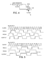
- FIG. 4 An arrangement with a single shift register is shown in Figure 4. As before, a multiplexer 6 selects either input A or B alternately under control of a clock 8. A single shifter register 2 now provides the input to both the A and B inputs of the MUX 6, with the A input being tapped from the shift register at a point one register from the end so that input A is an historical version in input B.
- This arrangement can also be used to divide by integer divisions. As shown in Figure 5, inter divisions are achieved with the register loaded as follows.
- the shift register stores: Register 1 1 0 0
- the shift register stores: Register 1 1 1 0 0
- the mark-space ratio is now uneven with a ratio of 5:4. Moreover, over many cycles, the high state is present more than the low state. Such an uneven mark-space ratio could cause noise and power problems, and so is not preferred.
- a single shift register as shown in Figure 4 cannot divide by a half integer factor. This is because division by a half integer requires the inputs on A and B to have a different sequence, whereas a single shift register in the arrangement shown can only ever produce the same sequence on A as on B, because each bit is presented first on B then on A.
- a single shift register digital divider arrangement embodying the invention and which can divide by half integers and produce a repeatable mark-space ratio is shown in Figure 6. Like components retain the same reference numbers as before.
- a multiplexer 6 is clocked by a clocking signal 8 which is also provided to a shift register 2 ( Figure 7) comprising a sequence of D-type flip flops which can be set and reset by SR control signals.
- the register is effectively variable in length by selecting the number of D-type flip flops activated and the loop point.
- Inputs A and B are thus from a single shift register as before. Input B passes direct to the multiplexer 6 via two D-type flip flops (for timing purposes described later)whereas input A passes through additional control logic circuitry 12 which provides additional functionality to detect low to high changes in input A and to use this additional information to allow odd and half integer division.
- control logic circuitry 12 comprises an edge detector 36 in the form of AND gate 14 for detecting changes in the bit sequence from the shift register from 0 to 1, a toggle or latch circuit 26, program logic circuit 40, timing circuitry and gates for providing inputs to the multiplexer 6.
- the edge detector provides a signal to the toggle circuit 26 which toggles to indicate the last status thereof.
- the program logic circuit 40 receives two inputs to allow the remaining gates to be configured, depending on whether odd, even or half integer division is to be performed.
- the control logic circuitry 12 is arranged as follows.
- a first AND gate 14 with an inverted input produces an output (A.B).
- a second AND gate 16 produces an output (A.B).
- the selection of whether or not the input A is presented at the output is achieved by the third AND gate 18 under control of the toggle and control circuitry.
- the input to AND gate 18 is 1, then the output is simply the input namely (A.B).
- the input to selecting OR gate 20 is (A.B) on one input and (A.B) on the other.
- the output is thus B on both channels X and Y to the multiplexer 6.
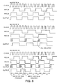
- the output of the multiplexer is simply B and so the pattern of digits in the shift register is simply chosen for the appropriate division e.g. (1100 1100) for divide by four as shown in Figure 8(a). All other even divisions follow the same pattern.
- AND gate 18 has the input of AND gate 18 as 1 so that the output follows the input with the result that the input to the multiplexer 6 is B on both X and Y inputs.
- the setting of AND gate 18 to have one input as 1 (or 0) is achieved by selection functionality provided by control logic OR gate 22 and control logic AND gate 24 with respective inputs labelled "EVEN” and "HALF-NOT-ODD". These inputs are set according to the following control logic: EVEN HALF-NOT-ODD FUNCTION X 0 Divide odd whole number (e.g. divide 5) 0 1 Divide half ratio (e.g. divide 3.5) 1 1 Divide even whole number (e.g. divide 6)
- OR gate 22 when dividing by an even whole number, the input to OR gate 22 is 1 and so the output is necessarily 1.
- the output given depends on the status of the D-type flip flop circuitry as now will be described.
- the toggle circuitry 26 comprises two AND gates 28, 30 with on inverting input, an OR gate 32 and a D-type flip-flop 34.
- the toggle itself receives a single input: ( A .B).
- the sequence of bits in the register changes from 0 to 1, the input to the multiplexer on X is B, otherwise, the input is (A.B).
- the D-type flip flop toggles every time a change in the sequence from 0 to 1 is detected so that the output is alternately 0 and 1 at changes in the bit sequence, and the input to the multiplexer an X is alternately (A.B) and B.
- X alternately (A.B) and B.
- the mark-space ratio for half division is not exactly equal (as shown) with a ratio of 3:4, but over two cycles is "even" in the sense that the output is high for as long as it is low. As previously noted, this can be important for power considerations.
- the toggling operation can be understood more fully by referring to Figure 9.
- the high/low status at points A to H are labelled and noted at Table 2.
- the reference HNEXT is the status at H after the next clock cycle.
- the output H goes to 1 when the input is 1, and stays at 1 until the input is next 1 when it goes to zero. Effectively, the whole circuit toggles from 1 to 0 and 0 to 1 alternately when the input is 1.
- the input is ( A .B) which, as previously described, is only high when a change in the bit register sequence from 0 to 1 is detected
- the D-type flip flop circuit toggles from 0 to 1 and 1 to 0 when changes in the bit sequence from 0 to 1 are detected.
- alternate "edges" in the output are effectively "deleted” as previously shown and described in relation to Figure 8(c).
- the digital divider includes elements which perform the following logical functions:
- the functions are provided (referring again to Figure 6) by the AND gate 14 functioning as an edge detector, D-type flip flop circuitry 26 functioning as an alternate edge selector, control logic to allow the circuit to be programmed according to the appropriate division and a "deleter" to make the output 0 at selected edges.
- the timing circuitry 38 comprises 3 D-type flip flops arranged with one in the X channel and one in the Y channel. This is to compensate the timing which is delayed by the D-type flip flop 34 and other components.
- a frequency divider embodying phase control according to the invention is shown in Figure 10.
- the divider comprises a circulating shift register 42 whose operation is similar to the shift register previously described.
- the sequence of bits in the shift register is tapped off and provided to control logic 112 which in turn provides an input to a multiplexer 48 again in a similar fashion to previously described.
- control logic 112 which in turn provides an input to a multiplexer 48 again in a similar fashion to previously described.
- a variable tap off point on the shift register 42 is provided for coarse phase control and the control logic 46 includes additional functionality for fine phase control. The coarse control of phase will be described first.
- the circulating shift register is loaded with the bit sequence of 1's and 0's depending upon the divide ratio required, as previously described and the number of bits of the register or "depth" controlled by the depth line 45.
- the bit sequence is cyclical in the register on circulating line 43, under control of clock signal 8.
- the output from the shift register 42 can be chosen at any tap off point under control of a tap off shift register 44 and combinatorial logic 46, with a combination of temporarily stopping circulation of the register 42 and altering the effective tap off point with tap off shift register 44 and combinatorial logic 46. This allows “coarse” control by which we mean varying the output clock phase in steps of one input clock cycle.
- the circulating shift register is shown in greater detail in Figure 11 and comprises a series of D type flip-flops 48, each initially loaded with a 0 or 1 according to the appropriate sequence. Upon loading the last flip-flop in the sequence, the feedback signal is provided to the first on circulating line 43. The output data from one flip-flop 48 is the source for the next flip-flop. Now each flip-flop has its input provided by a series of 3 multiplexers 49, 50, 51 which can selectively provide each Dtype with an input from the previous Dtype in the chain, or provide the output of the Dtype to its own input.
- the shift register is effectively paused by sourcing each flip-flop with a feedback of its own output data.
- each multiplexer 49 at the input of each flip-flop is switched so that the output is provided to the input of each flip-flop.
- the normal operation of the register is to shift to the right, so a pause gives a virtual shift right of the tap point, i.e. the output is phase shifted right by one cycle of the input clock.
- the tap off shift register 44 comprises a series of Dtype flip-flops 52 with inputs provided by two multiplexers 54,56.
- the tap off shift register 44 provides the output from one Dtype to the input of the next in a continuous loop including a feedback line 53.
- a single logic 1bit is input to the first Dtype initially, with the remaining Dtypes set to zero.
- This logic 1 is shifted through the flip-flops from output to input in turn and effectively shifts the tap off point of the circulating register to the point corresponding to the logic 1 though the combinatorial logic 46. If the tap off shiftregister 44 is paused, then the multiplexers 56 are switched so that each Dtype output is provided as its own input, thereby keeping the single logic 1 at a fixed point.
- the shifting of phase is thus achieved one way by pausing the circulating shift register (phase shifted right) or by allowing the tap off shift register to circulate (phase shifted left).
- an alternative would be to shift the tap off point in either direction with a bidirectional tap off shiftregister.
- This would require more multiplexers between Dtypes in the register which limits clock frequency, and so is not preferred.
- the combinatorial logic 46 is what governs the tap off point, and this is shown in greater detail in Figure 13. As shown, the tap off points for each Dtype in the circulating and tap off shiftregisters are passed to an AND function, shown as a series of AND gates 58.
- each AND gate will be zero except where the tap off shiftregister has a logic 1, in which case the output is the value of the corresponding bit in the circulating register.
- An OR function takes the output of the AND gates 58 and presents this as the output (shown as C in Figure 10).
- the moveable tap point allows for whole input clock cycle phase shifts ("coarse control") either left or right by logically moving the shift register left and right by logically or physically moving the tap point.
- coarse control further circuitry is provided in the control logic 112. This is required because the shift registers 42, 44 only shift on full clock cycles of the clock signal to be divided.
- the control logic 112 is shown in greater detail in Figure 14 and receives inputs A, B & C from the combinatorial logic 46.
- the input C is the direct output from the tap off point on the circulating shift register 42, whereas inputs B and A are delayed respectively by one and two clock periods by latches 64, 66. This provides outputs which are separated by clock periods as previously explained, but now there are three such outputs.
- the circuitry shares components in common with the circuit previously described in relation to Figure 6. Indeed, the circuit comprises verbatim the components from Figure 6 plus a mirror image circuit and so like components are labelled with the same numbers as before.
- the operation of the top half of the circuit is exactly as previously described and so will not be repeated.
- the inputs A and B are treated the same as before such that the output from multiplexer 6 is broadly as before providing even, odd and half integer division.
- the bottom half is a mirror image of the top and provides the same functionality, wherein an edge detector 136 comprising an AND gate 114 detects a change in the bit sequence of the signals B and C from the register 42.
- This signal provided to latch circuit 140 which operates exactly as previously described with reference to Figure 9, such that AND gates 128, 130 and OR gate 132 provide a signal to latch 134 so that the output of the latch 134 toggles to logic 1 when an edge is detected and remains at logic 1 until the next edge is detected to provide a signal which alternates with alternate edges.
- This is provided to OR gate 122 and AND gate 124 which function in exactly the same way as corresponding OR gate 22 and AND gate 24.
- the output from multiplexer 6 is therefore selectively either:
- the output from multiplexer 106 is selectively either:
- the multiplexers 6, 106 are governed by a phase select signal 152 to select between these signals which in combination with the output multiplexer 150 which is clocked by a clock signal 8 provides the output possibilities.
- A is a delayed version of B which is a delayed version of C each by one input clock period, and the output multiplexer 150 selects either the upper circuit or lower circuit every half cycle, the output is essentially phase shifted by a half cycle.
- the latches 40, 140 are logical 1 so that the output multiplexer alternately selects B (clock high); A (clock low) if the phase select is set high, or C (clock high); A (clock low) if the phase select is set low.
- B is a delayed version of C
- the output is essentially shifted. This is shown in Figure 15a, for division by 4.
- the inputs to the output multiplexer 150 are selected every half clock cycle and so are shown diagrammatically as shifted by one half clock cycle for ease of understanding the output signal obtained.
- the same principle applies for other divisions. For example, odd integer divisions would involve the output multiplexer selecting A.B (clock high); A (clock low) if the phase select is set high, or B.C (clock high); A (clock low).
- the shift FSM 160 is the control for shifting of the registers and changing the phase of the output clock to manage continuous half step phase changes in either direction.
- a number of states have to be taken into consideration. These are shifting left 170, shifting right 172, no shift 174, shifting left with phase change 176 and shifting right with phase change 176.
- the shifting of the clocks is caused by the assertion of shift_up (shift_left) or shift_down (shift right) inputs.
- the FSM outputs pause_up which pauses the circulating shift register and pause_down which causes the one hot tap off shift register to pause. These outputs cannot be asserted at the same time.
- the FSM After being in a state of shift_up or shift_down the FSM must make transition to the no_shift state in order for the output clock to settle with it's new phase sequence.
- the phase output is a bit that toggles when in a state of shift_up or shift_down. On assertion of shift_up or shift_down the phase is asserted. Therefore shifting the clocked edge up or down by half a clock period. If the shift_up or shift_down is asserted again the phase would be toggled and revert back to the original clocked edge and shift by a whole clock period. Therefore shifting the clocked edge by half a clock period. This is represented by means of a state diagram in Figure 16.
- Figure 17 shows a divide by 5 simulation waveforms. There is no shift_up/down so the register is continuously circulating. Note the one clock delay between C and B and then B and A. The input sequence has a 60:40 mark:space ratio and the output clock is 50:50. Also, note an odd divide ratio is first clocked off the rising edge. Note that in this diagram inputs A, B and C are correctly shown shifted by full input clock cycles, but that the outputs are selected every half clock cycle as before.
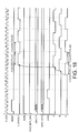
- Figure 18 shows the simulation waveforms for a divide by 6 with no shift_up/down asserted.
- the output clock is first clocked off a falling edge. Again, the inputs A, B and C are correctly shown shifted by full clock cycles.
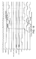
- Figure 19 shows the simulation waveforms for a divide by 4.5 with no shift_up/down asserted.
- divide by 4.5 the sequence is a divide by four followed by divide by three.
- the control logic achieves the 4.5 divide ratio by removing the first half clock cycle of sequence data on alternative periods of the output clock. Also the mark:space ratio alternates between output clock periods.
- Figure 20 shows the simulation waveforms for a divide by 6 ratio with shift_up function.
- the clockout is showing a divide by 6 ratio (logic1 for 3 clock cycles, logic0 for 3 clock cycles) when shift up is asserted.
- the phase is asserted which causes a half clock cycle shift and the clockout signal is clocked by a positive edge.
- the shift_up is asserted before the output clock settles at 6 clock cycles and the phase is toggled.
- the clockout is clocked by the original falling edge and the pause_up is asserted. This pauses the circulating shift register which gives one clock cycle extra of sequence data in A, B and C and therefore shifting one clock period giving a half clock cycle phase shift.
- the shift down functionality is similar. This asserts the phase in the same way to shift a half clock cycle and clockout is clocked off the opposite edge. If the shift_down is asserted again the phase is toggled which causes clockout to be clocked by the original edge. Then pause_down is asserted which causes the one hot tapoff shift register to pause which removes one clock cycle worth of sequence data from A, B and C and therefore shifting one clock period giving a half clock cycle phase shift.
Landscapes
- Pulse Circuits (AREA)
- Manipulation Of Pulses (AREA)
- Stabilization Of Oscillater, Synchronisation, Frequency Synthesizers (AREA)
Abstract
A digital frequency divider includes phase control of the
output signal in increments of whole or half cycles of the
input frequency. Whole cycle phase control is achieved by
varying (logically or physically) the tap off point of a
shift register loaded with a bit pattern for appropriate
division. Half cycle phase changes is achieved by a
multiplexer selecting one of two signals every half cycle.
Description
- The present invention relates to a digital frequency divider with a phase control, and in particular to a frequency divider with a shift register.
- In digital systems, integrated circuits (ICs) or chips are operated by pulses from a clock. In systems such as television receivers or decrypters, there can be many different chips each operating at a different clock frequency. The different regions operating at different frequencies are referred to as "clock domains". For example, one chip may operate as a master chip in a 166 MHz domain, with another store chip in a 133 MHz domain. In this situation, there is a need for two clock frequencies.
- One solution to the problem of providing different clock frequencies is to use a master frequency and produce the frequency for the store by diving the master clock frequency.
- We have appreciated that the frequency division should introduce a minimum noise into the clocking signal, and involve efficient use of circuitry. We have also appreciated that it would be useful to control the phase of a divided clock frequency. One known way of changing clock phase relative to one another is to use a delay line. However, we have appreciated that the maximum delays achievable with delay lines are small, and that they are prone to noise.
- Accordingly, there is provided a digital frequency divider for dividing a clock frequency and having a variable phase output comprising:
- a shift register for storing a bit sequence chosen according to a division factor and operating under control of a clock signal at a first frequency;
- tap off circuitry arranged to tap the shift register at one or more variable points and arranged to produce two or more signals representative of the bit sequence;
- control logic circuitry having at least two inputs arranged to receive the two or more signals representative of the bit sequence and arranged to provide at least two output signals; and
- a multiplexer arranged to receive the two output signals and to select one of the output signals in turn under control of the clock signal at the first frequency to thereby produce a clock output signal at a second frequency being a division of the first frequency;
- wherein the tap off circuitry and shift register are arranged such that the one or more tap off points of the shift register are variable in position along the bit sequence such that the clock output signal is variable in phase.
- The combining of phase control with the circuitry of a frequency divider is an efficient use of circuitry. Moreover, the phase control is wholly digital and allows infinite delay, both positive and negative, in either direction.
- An embodiment of the invention will now be described, by way of example only, in which:
- Figure 1:
- shows two shift register digital frequency divider;
- Figure 2:
- shows sequences for the two shift register divider for various divisions;
- Figure 3:
- shows sequences for division by various other factors;
- Figure 4:
- shows a single shift register digital frequency divider;
- Figure 5:
- shows various register sequences for the single shift register frequency divider of Figure 4;
- Figure 6:
- shows control logic circuitry;
- Figure 7:
- shows a shift register;
- Figure 8:
- shows various register sequences for the shift register and control circuitry of Figures 6 and 7;
- Figure 9:
- shows latch circuitry and its table of status;
- Figure 10:
- shows a frequency divider with phase control embodying the invention;
- Figure 11:
- shows the shift register of Figure 10 in greater detail;
- Figure 12:
- shows the tap off register of Figure 10 in greater detail;
- Figure 13:
- shows the combinatorial logic of Figure 10 in greater detail;
- Figure 14:
- shows the control logic of Figure 10 in greater detail;
- Figure 15:
- shows division by 4;
- Figure 16:
- shows a state diagram of the phase changes; and
- Figures 17 to 20:
- show timing diagrams for various division factors according to the invention.
- The embodiment of the invention comprises a frequency divider using a single shift register to perform division and additional components to control the phase of the output. The phase control is combined with the frequency divider itself resulting in an efficient use of circuitry. A digital frequency divider without phase control will first be described for ease of understanding with reference to Figures 1 to 9, followed by a description of a divider with phase control.
- A two shift register frequency divider is shown in figure 1, and comprises two variable
length shift registers digital clock signal 8. Although not shown, the shift registers are in fact rotatable so that the output is rotated back to the input whereby the contents of the register is rotated with each bit in turn presented at the output. The shift registers are arranged to progress on a change in the clock from low to high, whereas the multiplexer is simply level sensitive. The multiplexer thus selects Register A when the clock is high and Register B when the clock is low. - The output signal o/p is a division of the clock signal depending on the length and arrangement of bits in the shift register. The arrangement of bits in the registers for a simple division by two is shown in Figure 2. As can be seen, the contents of each register is a simple sequence of repeating (10101010....). In fact, a shift register containing the sequence (1010) may be used and rotated in a continuous loop.
- The two shift register divider works for other divisions, as shown in Figure 3. In Figure 3(a) division by a factor of 1½ is shown. The smallest units for each register are:
Register A 1 0 0 Register B 1 1 0 - Similarly Figure 3(b) shows
division 3 with the following registers:Register A 1 1 0 Register B 1 0 0 - Lastly, Figure 3(c) shows division by 4 with registers as follows:
Register A 1 1 0 0 Register B 1 1 0 0 - It will be noted that the ratio between highs and lows (the mark-space ratio) for division by half integer numbers is uneven, but over two or more cycles produces a high state and low state for equal durations. For even or odd integer division the mark-space ratio is even. To allow for differing high/low sequences for different divisions, the shift registers are variable length. As can be seen the higher the division factor, the longer the shift register needs to be.
- An arrangement with a single shift register is shown in Figure 4. As before, a
multiplexer 6 selects either input A or B alternately under control of aclock 8. Asingle shifter register 2 now provides the input to both the A and B inputs of theMUX 6, with the A input being tapped from the shift register at a point one register from the end so that input A is an historical version in input B. This arrangement can also be used to divide by integer divisions. As shown in Figure 5, inter divisions are achieved with the register loaded as follows. - For division by 4, as shown in Figure 5(a) the shift register stores:
Register 1 1 0 0 - For division by 5, as shown in Figure 5(b) the shift register stores:
Register 1 1 1 0 0 - However, for division by 5, the mark-space ratio is now uneven with a ratio of 5:4. Moreover, over many cycles, the high state is present more than the low state. Such an uneven mark-space ratio could cause noise and power problems, and so is not preferred.
- A single shift register as shown in Figure 4 cannot divide by a half integer factor. This is because division by a half integer requires the inputs on A and B to have a different sequence, whereas a single shift register in the arrangement shown can only ever produce the same sequence on A as on B, because each bit is presented first on B then on A.
- A single shift register digital divider arrangement embodying the invention and which can divide by half integers and produce a repeatable mark-space ratio is shown in Figure 6. Like components retain the same reference numbers as before. A
multiplexer 6 is clocked by aclocking signal 8 which is also provided to a shift register 2 (Figure 7) comprising a sequence of D-type flip flops which can be set and reset by SR control signals. The register is effectively variable in length by selecting the number of D-type flip flops activated and the loop point. - Inputs A and B are thus from a single shift register as before. Input B passes direct to the
multiplexer 6 via two D-type flip flops (for timing purposes described later)whereas input A passes through additionalcontrol logic circuitry 12 which provides additional functionality to detect low to high changes in input A and to use this additional information to allow odd and half integer division. - In broad terms, the
control logic circuitry 12 comprises anedge detector 36 in the form of ANDgate 14 for detecting changes in the bit sequence from the shift register from 0 to 1, a toggle orlatch circuit 26,program logic circuit 40, timing circuitry and gates for providing inputs to themultiplexer 6. The edge detector provides a signal to thetoggle circuit 26 which toggles to indicate the last status thereof. Theprogram logic circuit 40 receives two inputs to allow the remaining gates to be configured, depending on whether odd, even or half integer division is to be performed. - The
control logic circuitry 12 is arranged as follows. A first ANDgate 14 with an inverted input produces an output (A.B). A second ANDgate 16 produces an output (A.B). With the additional knowledge that A is a historical version of B shifted by one bit, we know that:
(A .B)=1 if A=0 and B=1, i.e. a rising edge is detected in the shift register sequence. - Similarly, we know that:
(A.B)=1 if A=1 and B=1, i.e. the sequence is not a rising or falling edge. - This information in itself would be sufficient to perform odd integer division by configuring the circuit to always remove the first half clock cycle of sequence data from the output. This would make the mark-space ratio 4.5:4.5 rather than 5:4 that we had before. However, if this were done, then even division would have an irregular mark-space ratio. Further, division by half integers would not operate correctly. Accordingly, in addition to detecting low to high changes, the control logic circuitry determines alternate low to high changes to allow removal of the first half clock cycle of sequence data on alternate periods. This configurability is provided by a function in the
circuit 12 to detect the rising edge indication and a function to select deletion of bits depending on whether the division is even, odd or half integer. - The selection of whether or not the input A is presented at the output is achieved by the third AND
gate 18 under control of the toggle and control circuitry. In the event that the input to ANDgate 18 is 1, then the output is simply the input namely (A.B). In this case the input to selectingOR gate 20 is (A.B) on one input and (A.B) on the other. The output of selectingOR gate 20 is therefore:
(A .B)+(A.B)
which is = B.
The output is thus B on both channels X and Y to themultiplexer 6. The output of the multiplexer is simply B and so the pattern of digits in the shift register is simply chosen for the appropriate division e.g. (1100 1100) for divide by four as shown in Figure 8(a). All other even divisions follow the same pattern. - The example given above for even division has the input of AND
gate 18 as 1 so that the output follows the input with the result that the input to themultiplexer 6 is B on both X and Y inputs. The setting of ANDgate 18 to have one input as 1 (or 0) is achieved by selection functionality provided by control logic ORgate 22 and control logic ANDgate 24 with respective inputs labelled "EVEN" and "HALF-NOT-ODD". These inputs are set according to the following control logic:EVEN HALF-NOT- ODD FUNCTION X 0 Divide odd whole number (e.g. divide 5) 0 1 Divide half ratio (e.g. divide 3.5) 1 1 Divide even whole number (e.g. divide 6) - As can be seen, when dividing by an even whole number, the input to OR
gate 22 is 1 and so the output is necessarily 1. The inputs to ANDgate 24 are both 1 and so the output is 1 so that ANDgate 18 is effectively ignored (becomes an input follower) providing the output (A .B)+(A.B)=B fromOR gate 20 as described above. - As can also be seen, with the input of HALF-NOT-ODD as zero to AND
gate 24, the output ANDgate 24 is also zero, further setting the output of ANDgate 18 to zero with the result that selectingOR gate 20 becomes an input follower with an output (A.B). The inputs to the multiplexer are B and (A.B) with the result as shown in Figure 8(b) for division by 5; an even mark-space ratio is provided. Effectively, the first half clock cycle at each change from 0 to 1 is "deleted" in the sense that the input to the multiplexer is zero. This is because (A.B)=0 whenever there is a change for 0 to 1 in the bit sequence, because B=1 and A=0. The pattern in the shift register is (11100) and all other odd divisions follow the same patterning (1111000) for division by 7. - The case for division by half ratios involves
toggle circuitry 26 as can now be seen. With control logic inputs EVEN = 0 and HALF-NOT-ODD = 1, bothOR gate 22 and ANDgate 24 become input followers so that the output oftoggle circuit 26 is presented to ANDgate 18. Following this through, the output of ANDgate 18 is either 0 or (A .B) with the result that one of two possible outputs fromOR gate 20 are given: - (i) A.B (if D-type flip flop output = 0)
- (ii) (
A .B) + (A.B) = B (if D-type flip flop output = 1) -
- The output given depends on the status of the D-type flip flop circuitry as now will be described.
- The
toggle circuitry 26 comprises two ANDgates OR gate 32 and a D-type flip-flop 34. The toggle itself receives a single input: (A .B). The D-type 34 feeds its input back to the ANDgates gate 28 produces output = 1 so the input to the D-type = 1. Thus, a change in sequence from A = 0 to A = 1 is sampled and produces a D-type flip flop output = 1. Thus, when the sequence of bits in the register changes from 0 to 1, the input to the multiplexer on X is B, otherwise, the input is (A.B). The D-type flip flop toggles every time a change in the sequence from 0 to 1 is detected so that the output is alternately 0 and 1 at changes in the bit sequence, and the input to the multiplexer an X is alternately (A.B) and B. As a result, as shown in Figure 8(c), alternate portions of the first half cycle of the output shown as "X" are effectively "deleted" in the sense that without toggle operation, the output would simply be B and the output would be 1. - The mark-space ratio for half division is not exactly equal (as shown) with a ratio of 3:4, but over two cycles is "even" in the sense that the output is high for as long as it is low. As previously noted, this can be important for power considerations.
- The toggling operation can be understood more fully by referring to Figure 9. The high/low status at points A to H are labelled and noted at Table 2. The reference HNEXT is the status at H after the next clock cycle. As can be seen, the output H goes to 1 when the input is 1, and stays at 1 until the input is next 1 when it goes to zero. Effectively, the whole circuit toggles from 1 to 0 and 0 to 1 alternately when the input is 1. Now since the input is (
A .B) which, as previously described, is only high when a change in the bit register sequence from 0 to 1 is detected, the D-type flip flop circuit toggles from 0 to 1 and 1 to 0 when changes in the bit sequence from 0 to 1 are detected. As a result, alternate "edges" in the output are effectively "deleted" as previously shown and described in relation to Figure 8(c). - In summary, the digital divider includes elements which perform the following logical functions:
- (i) a change in the register bit sequence from 0 to 1 is detected (known as an "edge");
- (ii) edges selected; and
- (iii) edges for first half clock cycle "deleted" in the sense that the output to the multiplexer is 0.
-
- The functions are provided (referring again to Figure 6) by the AND
gate 14 functioning as an edge detector, D-typeflip flop circuitry 26 functioning as an alternate edge selector, control logic to allow the circuit to be programmed according to the appropriate division and a "deleter" to make theoutput 0 at selected edges. - The
timing circuitry 38 comprises 3 D-type flip flops arranged with one in the X channel and one in the Y channel. This is to compensate the timing which is delayed by the D-type flip flop 34 and other components. - Clearly, other arrangements of gates and other components such as Boolean equivalents of those described may be used and are within the scope of the invention. In particular, the
symbols - A frequency divider embodying phase control according to the invention is shown in Figure 10. The divider comprises a circulating
shift register 42 whose operation is similar to the shift register previously described. The sequence of bits in the shift register is tapped off and provided to controllogic 112 which in turn provides an input to amultiplexer 48 again in a similar fashion to previously described. In addition, however, a variable tap off point on theshift register 42 is provided for coarse phase control and thecontrol logic 46 includes additional functionality for fine phase control. The coarse control of phase will be described first. - The circulating shift register is loaded with the bit sequence of 1's and 0's depending upon the divide ratio required, as previously described and the number of bits of the register or "depth" controlled by the
depth line 45. In normal operation, the bit sequence is cyclical in the register on circulatingline 43, under control ofclock signal 8. The output from theshift register 42 can be chosen at any tap off point under control of a tap offshift register 44 andcombinatorial logic 46, with a combination of temporarily stopping circulation of theregister 42 and altering the effective tap off point with tap offshift register 44 andcombinatorial logic 46. This allows "coarse" control by which we mean varying the output clock phase in steps of one input clock cycle. - The circulating shift register is shown in greater detail in Figure 11 and comprises a series of D type flip-
flops 48, each initially loaded with a 0 or 1 according to the appropriate sequence. Upon loading the last flip-flop in the sequence, the feedback signal is provided to the first on circulatingline 43. The output data from one flip-flop 48 is the source for the next flip-flop. Now each flip-flop has its input provided by a series of 3multiplexers multiplexer 49 at the input of each flip-flop is switched so that the output is provided to the input of each flip-flop. The normal operation of the register is to shift to the right, so a pause gives a virtual shift right of the tap point, i.e. the output is phase shifted right by one cycle of the input clock. - To shift the phase left, the tap off point should be shifted left, and this is achieved by the tap off
shift register 44 shown in greater detail in Figure 12. The tap offshiftregister 44 comprises a series of Dtype flip-flops 52 with inputs provided by twomultiplexers shift register 42, the tap offshift register 44 provides the output from one Dtype to the input of the next in a continuous loop including afeedback line 53. A single logic 1bit is input to the first Dtype initially, with the remaining Dtypes set to zero. Thislogic 1 is shifted through the flip-flops from output to input in turn and effectively shifts the tap off point of the circulating register to the point corresponding to thelogic 1 though thecombinatorial logic 46. If the tap offshiftregister 44 is paused, then themultiplexers 56 are switched so that each Dtype output is provided as its own input, thereby keeping thesingle logic 1 at a fixed point. - The shifting of phase is thus achieved one way by pausing the circulating shift register (phase shifted right) or by allowing the tap off shift register to circulate (phase shifted left). Of course, an alternative would be to shift the tap off point in either direction with a bidirectional tap off shiftregister. However, this would require more multiplexers between Dtypes in the register which limits clock frequency, and so is not preferred. The
combinatorial logic 46 is what governs the tap off point, and this is shown in greater detail in Figure 13. As shown, the tap off points for each Dtype in the circulating and tap off shiftregisters are passed to an AND function, shown as a series of ANDgates 58. The output of each AND gate will be zero except where the tap off shiftregister has alogic 1, in which case the output is the value of the corresponding bit in the circulating register. An OR function takes the output of the ANDgates 58 and presents this as the output (shown as C in Figure 10). - The moveable tap point allows for whole input clock cycle phase shifts ("coarse control") either left or right by logically moving the shift register left and right by logically or physically moving the tap point. To provide half clock cycle phase shifts ("fine" control), further circuitry is provided in the
control logic 112. This is required because the shift registers 42, 44 only shift on full clock cycles of the clock signal to be divided. - The
control logic 112 is shown in greater detail in Figure 14 and receives inputs A, B & C from thecombinatorial logic 46. The input C is the direct output from the tap off point on the circulatingshift register 42, whereas inputs B and A are delayed respectively by one and two clock periods bylatches - The operation of the top half of the circuit is exactly as previously described and so will not be repeated. The inputs A and B are treated the same as before such that the output from
multiplexer 6 is broadly as before providing even, odd and half integer division. The bottom half is a mirror image of the top and provides the same functionality, wherein anedge detector 136 comprising an ANDgate 114 detects a change in the bit sequence of the signals B and C from theregister 42. The signal B is a delayed version of signal C and so the output of AND gate 114 (B.C) = 1 when the sequence is at an "edge", with B=0 and C=1. This signal provided to latchcircuit 140 which operates exactly as previously described with reference to Figure 9, such that ANDgates OR gate 132 provide a signal to latch 134 so that the output of thelatch 134 toggles tologic 1 when an edge is detected and remains atlogic 1 until the next edge is detected to provide a signal which alternates with alternate edges. This is provided to ORgate 122 and ANDgate 124 which function in exactly the same way as corresponding ORgate 22 and ANDgate 24. - The output from
multiplexer 6 is therefore selectively either: - (i) A.B (if
latch circuit 40 output = 0) - (ii) (
A .B) + (A.B) = B (iflatch circuit 40 output = 1); or - (iii) A (The state of the latch output depends on the EVEN and HALF-NOT-ODD signals and the state of the toggle circuit as previously described).
-
- Similarly, the output from
multiplexer 106 is selectively either: - (i) B.C (If
latch circuit 140 output = 0) - (ii) (
B .C)+(B.C)=C (iflatch circuit 140 output=1); or - (iii) A
-
- Now the
multiplexers select signal 152 to select between these signals which in combination with theoutput multiplexer 150 which is clocked by aclock signal 8 provides the output possibilities. - If phase select high:
- (i) A.B (if
latch 40 = 0) - (ii) B (if
latch 40 = 1); or - (iii) A
-
- If phase select low:
- (i) A
- (ii) B.C (if
latch 140 = 0); or - (iii) C (if
latch 140 = 1) -
- Now since A is a delayed version of B which is a delayed version of C each by one input clock period, and the
output multiplexer 150 selects either the upper circuit or lower circuit every half cycle, the output is essentially phase shifted by a half cycle. This can be seen most simply for even division in which thelatches output multiplexer 150 are selected every half clock cycle and so are shown diagrammatically as shifted by one half clock cycle for ease of understanding the output signal obtained. The same principle applies for other divisions. For example, odd integer divisions would involve the output multiplexer selecting A.B (clock high); A (clock low) if the phase select is set high, or B.C (clock high); A (clock low). - Now consider half integer division. In the previous non-phase shift enabled single register divider, the appropriate register sequence for division by 3½ was (1100110). Because moving the tap point effectively skips one of the bits in the sequence, the single '0' could be missed by the control logic. This would cause the control logic to miss a 0 to 1 transition, resulting in the toggle output being the inverse of it's correct value. This in turn will result in an incorrect mark space ratio. To ensure correct operation, the bit pattern should always have at least pairs of values i.e. 1100 and not 01011.
- There is thus a limitation that values of upwards of 3½ for division factor must be used.
- Turning again to Figure 10, the last component to consider is the
shift FSM 160. - The
shift FSM 160 is the control for shifting of the registers and changing the phase of the output clock to manage continuous half step phase changes in either direction. A number of states have to be taken into consideration. These are shifting left 170, shifting right 172, noshift 174, shifting left withphase change 176 and shifting right withphase change 176. The shifting of the clocks is caused by the assertion of shift_up (shift_left) or shift_down (shift right) inputs. The FSM outputs pause_up which pauses the circulating shift register and pause_down which causes the one hot tap off shift register to pause. These outputs cannot be asserted at the same time. - After being in a state of shift_up or shift_down the FSM must make transition to the no_shift state in order for the output clock to settle with it's new phase sequence.
- The phase output is a bit that toggles when in a state of shift_up or shift_down. On assertion of shift_up or shift_down the phase is asserted. Therefore shifting the clocked edge up or down by half a clock period. If the shift_up or shift_down is asserted again the phase would be toggled and revert back to the original clocked edge and shift by a whole clock period. Therefore shifting the clocked edge by half a clock period. This is represented by means of a state diagram in Figure 16.
- Figure 17 shows a divide by 5 simulation waveforms. There is no shift_up/down so the register is continuously circulating. Note the one clock delay between C and B and then B and A. The input sequence has a 60:40 mark:space ratio and the output clock is 50:50. Also, note an odd divide ratio is first clocked off the rising edge. Note that in this diagram inputs A, B and C are correctly shown shifted by full input clock cycles, but that the outputs are selected every half clock cycle as before.
- Figure 18 shows the simulation waveforms for a divide by 6 with no shift_up/down asserted. When implementing a even divide ratio the output clock is first clocked off a falling edge. Again, the inputs A, B and C are correctly shown shifted by full clock cycles.
- Figure 19 shows the simulation waveforms for a divide by 4.5 with no shift_up/down asserted. When implementing a half divide the sequence is more complicated. In the case of divide by 4.5 the sequence is a divide by four followed by divide by three. The control logic achieves the 4.5 divide ratio by removing the first half clock cycle of sequence data on alternative periods of the output clock. Also the mark:space ratio alternates between output clock periods.
- Lastly, Figure 20 shows the simulation waveforms for a divide by 6 ratio with shift_up function. The clockout is showing a divide by 6 ratio (logic1 for 3 clock cycles, logic0 for 3 clock cycles) when shift up is asserted. For this condition (see state diagram, Figure 16) the phase is asserted which causes a half clock cycle shift and the clockout signal is clocked by a positive edge. Again the shift_up is asserted before the output clock settles at 6 clock cycles and the phase is toggled. On toggling the phase the clockout is clocked by the original falling edge and the pause_up is asserted. This pauses the circulating shift register which gives one clock cycle extra of sequence data in A, B and C and therefore shifting one clock period giving a half clock cycle phase shift.
- The shift down functionality is similar. This asserts the phase in the same way to shift a half clock cycle and clockout is clocked off the opposite edge. If the shift_down is asserted again the phase is toggled which causes clockout to be clocked by the original edge. Then pause_down is asserted which causes the one hot tapoff shift register to pause which removes one clock cycle worth of sequence data from A, B and C and therefore shifting one clock period giving a half clock cycle phase shift.
Claims (21)
- A digital frequency divider for dividing a clock frequency and having a variable phase output, comprising:a shift register for storing a bit sequence chosen according to a division factor and operating under control of a clock signal at a first frequency;tap off circuitry arranged to tap the shift register at one or more variable points and arranged to produce two or more signals representative of the bit sequence;control logic circuitry having at least two inputs respectively arranged to receive the two or more signals representative of the bit sequence and arranged to provide at least two output signals; anda multiplexer arranged to receive the two output signals and to select one of the output signals in turn under control of the clock signal at the first frequency to thereby produce a clock output signal at a second frequency being a division of the first frequency;wherein the tap off circuitry and shift register are arranged such that the one or more tap off points of the shift register are variable in position along the bit sequence such that the clock output signal is variable in phase.
- A digital frequency divider according to claim 1, wherein the shift register is operable in a pause mode, whereby the bit sequence remains in fixed locations in the shift register thereby logically varying the one or more tap off points.
- A digital frequency divider according to claim 1 or 2, wherein tap off circuitry comprises a tap off register with a moveable tap off bit sequence and combinatorial logic to logically tap the shift register at one or more points corresponding to logic 1 in the tap off register.
- A digital frequency divider according to claim 3, wherein the tap off circuitry includes an AND function for combining bits from the shift register with bits from the tap off register thereby logically tapping the shift register at points corresponding to logic 1 in the tap off bit sequence.
- A digital frequency divider according to claim 3 or 4, wherein the tap off bit sequence is moveable in either direction.
- A digital frequency divider according to claim 3 or 4, wherein the tap off bit sequence is moveable in one direction to produce a phase shift in a first direction in the output clock, and the shift register is operable in a pause mode thereby logically varying the tap off point and consequently the phase to produce a shift in a second opposite direction.
- A digital frequency divider according to any preceding claim, wherein the tap off circuitry includes one or more delays arranged so that the at least two signals are delayed versions of one another delayed by one or more clock periods at the first frequency.
- A digital frequency divider according to any preceding claim, wherein the tap off circuitry is arranged to produce three signals representative of the bit sequence, a first one of the three signals having no delay, a second one of the three signals having a delay by one clock period and a third one of the three signals having a delay by two clock periods.
- A digital frequency divider according to claim 8, wherein the control logic circuitry has three inputs, are each arranged to receive the first, second and third signals representative of the bit sequence, and comprising selection circuitry arranged to produce the two output signals from the three signals representative of the bit sequence.
- A digital frequency divider according to claim 8 or 9, wherein the selection circuitry comprises two selecting multiplexers arranged to produce the two output signals selectably providing the two output signals shifted by one half clock cycle at the first frequency.
- A digital frequency divider according to claim 8, 9 or 10, wherein the control logic circuitry comprises first and second detectors, the first detector being configured to detect a change in the bit sequence between 0 and 1 in the first and second signals representative of the bit sequence, the second detector being configured to detect a change in the bit sequence between 0 and 1 in the second and third signals representative of the bit sequence.
- A digital frequency divider according to claim 11, wherein each detector comprises an AND gate arranged to receive one of the three signals inverted and one of the other three signals to thereby produce a logic 1 when a change in the bit sequence between 0 and 1 is detected.
- A digital frequency divider according any of claims 11 to 12, wherein the control logic circuitry is arranged to produce 1 as a first one of the outputs when a change in the bit sequence is detected for even division.
- A digital frequency divider according to any of claims 11 to 13, wherein the control logic circuitry is arranged to produce a 0 as a first one of the outputs when a change in the bit sequence is detected for odd division.
- A digital frequency divider according to any of claims 11 to 14, wherein the control logic circuitry is arranged to alternately produce a 0 then 1 as a first one of the outputs when a change in the bit sequence is detected for half integer division.
- A digital frequency divider according to any of claims 11 to 15, wherein the control logic circuitry includes program circuitry for indicating one of three states respectively for even, odd or half integer division.
- A digital frequency divider according to claim 16, wherein the program circuitry provides a 1 for even division, 0 for odd division or alternately 1 and 0 for half integer division.
- A digital frequency divider according to claim 16 or 17, wherein the program circuitry comprises an OR gate and AND gate in sequence each with one control input.
- A digital frequency divider according to claims 16 or 17, wherein the control logic circuitry includes a toggle arranged to receive a signal from the detector and to alternately produce 0 or 1 on receiving an indication of a change in the bit sequence, and to provide the alternate 0 or 1 to the control logic circuitry.
- A digital frequency divider according to any preceding claim, wherein the multiplexer is arranged to select a first one of the output signals when the clock signal is high and a second one of the output signals when the clock is low.
- A digital frequency divider according to any preceding claim, wherein the a shift register is arranged to shift in either direction and the tap off circuitry is arranged to tap the shift register at one or more points.
Priority Applications (2)
| Application Number | Priority Date | Filing Date | Title |
|---|---|---|---|
| EP01302735A EP1244214A1 (en) | 2001-03-23 | 2001-03-23 | Phase control digital frequency divider |
| US10/104,994 US6696870B2 (en) | 2001-03-23 | 2002-03-22 | Phase control digital frequency divider |
Applications Claiming Priority (1)
| Application Number | Priority Date | Filing Date | Title |
|---|---|---|---|
| EP01302735A EP1244214A1 (en) | 2001-03-23 | 2001-03-23 | Phase control digital frequency divider |
Publications (1)
| Publication Number | Publication Date |
|---|---|
| EP1244214A1 true EP1244214A1 (en) | 2002-09-25 |
Family
ID=8181823
Family Applications (1)
| Application Number | Title | Priority Date | Filing Date |
|---|---|---|---|
| EP01302735A Withdrawn EP1244214A1 (en) | 2001-03-23 | 2001-03-23 | Phase control digital frequency divider |
Country Status (2)
| Country | Link |
|---|---|
| US (1) | US6696870B2 (en) |
| EP (1) | EP1244214A1 (en) |
Cited By (1)
| Publication number | Priority date | Publication date | Assignee | Title |
|---|---|---|---|---|
| WO2005036751A1 (en) * | 2003-10-13 | 2005-04-21 | Koninklijke Philips Electronics N.V. | A frequency divider and an electronic device incorporating such a frequency divider |
Families Citing this family (12)
| Publication number | Priority date | Publication date | Assignee | Title |
|---|---|---|---|---|
| EP1405417B1 (en) * | 2001-07-06 | 2005-02-09 | Telefonaktiebolaget LM Ericsson (publ) | Fractional frequency divider |
| US7622965B2 (en) * | 2006-01-31 | 2009-11-24 | International Business Machines Corporation | Dual-edge shaping latch/synchronizer for re-aligning edges |
| US7474134B2 (en) * | 2006-05-18 | 2009-01-06 | International Business Machines Corporation | Radiation hardened programmable phase frequency divider |
| US7801263B2 (en) * | 2007-02-12 | 2010-09-21 | Marvell Israel (M.I.S.L.) Ltd. | Clock divider with a rational division factor |
| JP5098358B2 (en) * | 2007-02-22 | 2012-12-12 | 富士通セミコンダクター株式会社 | Processing element and reconfigurable circuit having the same |
| US8093929B2 (en) * | 2010-03-02 | 2012-01-10 | Freescale Semiconductor, Inc. | Programmable digital clock signal frequency divider module and modular divider circuit |
| US8368436B1 (en) * | 2010-10-29 | 2013-02-05 | Maxim Integrated, Inc. | Programmable frequency synthesizer with I/Q outputs |
| CN102055465A (en) * | 2010-12-09 | 2011-05-11 | 山东大学 | Frequency divider capable of configuring any integer and half-integer and method using same |
| WO2012127487A1 (en) * | 2011-03-23 | 2012-09-27 | Tejas Network Limited | An apparatus for glitch-free clock switching and a method thereof |
| CN102508804A (en) * | 2011-10-20 | 2012-06-20 | 豪威科技(上海)有限公司 | Secure digital (SD)/secure digital input and output (SDIO) master controller |
| CN109765828B (en) * | 2019-02-25 | 2023-08-25 | 成都芯进电子有限公司 | Magnetic resistance type sensor chip time sequence control circuit and control method |
| EP4089435B1 (en) | 2021-05-12 | 2025-05-28 | Nxp B.V. | Radar system |
Citations (4)
| Publication number | Priority date | Publication date | Assignee | Title |
|---|---|---|---|---|
| JPH01120810A (en) * | 1987-11-04 | 1989-05-12 | Sumitomo Metal Ind Ltd | Microwave plasma production device |
| US5889436A (en) * | 1996-11-01 | 1999-03-30 | National Semiconductor Corporation | Phase locked loop fractional pulse swallowing frequency synthesizer |
| US5970110A (en) * | 1998-01-09 | 1999-10-19 | Neomagic Corp. | Precise, low-jitter fractional divider using counter of rotating clock phases |
| US6114914A (en) * | 1999-05-19 | 2000-09-05 | Cypress Semiconductor Corp. | Fractional synthesis scheme for generating periodic signals |
Family Cites Families (4)
| Publication number | Priority date | Publication date | Assignee | Title |
|---|---|---|---|---|
| FR2105319A5 (en) * | 1970-08-21 | 1972-04-28 | Sescosem | |
| FR2522826B1 (en) * | 1982-03-05 | 1986-01-31 | Thomson Csf | DEVICE FOR DIGITAL GENERATION OF A FREQUENCY MODULATED SIGNAL AND RADIO FREQUENCY DEVICE COMPRISING SUCH A DIGITAL DEVICE |
| US5052031A (en) * | 1990-08-14 | 1991-09-24 | At&T Bell Laboratories | Phase locked loop including non-integer multiple frequency reference signal |
| JP2966491B2 (en) * | 1990-08-20 | 1999-10-25 | 株式会社アドバンテスト | Broadband pulse pattern generator |
-
2001
- 2001-03-23 EP EP01302735A patent/EP1244214A1/en not_active Withdrawn
-
2002
- 2002-03-22 US US10/104,994 patent/US6696870B2/en not_active Expired - Lifetime
Patent Citations (4)
| Publication number | Priority date | Publication date | Assignee | Title |
|---|---|---|---|---|
| JPH01120810A (en) * | 1987-11-04 | 1989-05-12 | Sumitomo Metal Ind Ltd | Microwave plasma production device |
| US5889436A (en) * | 1996-11-01 | 1999-03-30 | National Semiconductor Corporation | Phase locked loop fractional pulse swallowing frequency synthesizer |
| US5970110A (en) * | 1998-01-09 | 1999-10-19 | Neomagic Corp. | Precise, low-jitter fractional divider using counter of rotating clock phases |
| US6114914A (en) * | 1999-05-19 | 2000-09-05 | Cypress Semiconductor Corp. | Fractional synthesis scheme for generating periodic signals |
Non-Patent Citations (1)
| Title |
|---|
| PATENT ABSTRACTS OF JAPAN vol. 013, no. 364 (E - 805) 14 August 1989 (1989-08-14) * |
Cited By (3)
| Publication number | Priority date | Publication date | Assignee | Title |
|---|---|---|---|---|
| WO2005036751A1 (en) * | 2003-10-13 | 2005-04-21 | Koninklijke Philips Electronics N.V. | A frequency divider and an electronic device incorporating such a frequency divider |
| JP2007508767A (en) * | 2003-10-13 | 2007-04-05 | コーニンクレッカ フィリップス エレクトロニクス エヌ ヴィ | Frequency divider and electronic device incorporating the frequency divider |
| US7304512B2 (en) | 2003-10-13 | 2007-12-04 | Nxp B.V. | Frequency divider and an electronic device incorporating such a frequency divider |
Also Published As
| Publication number | Publication date |
|---|---|
| US6696870B2 (en) | 2004-02-24 |
| US20020171459A1 (en) | 2002-11-21 |
Similar Documents
| Publication | Publication Date | Title |
|---|---|---|
| US5268656A (en) | Programmable clock skew adjustment circuit | |
| US5036230A (en) | CMOS clock-phase synthesizer | |
| US5287025A (en) | Timing control circuit | |
| US6696870B2 (en) | Phase control digital frequency divider | |
| US6859884B1 (en) | Method and circuit for allowing a microprocessor to change its operating frequency on-the-fly | |
| US5355037A (en) | High performance digital phase locked loop | |
| US7378893B1 (en) | Circuit and method for digital delay and circuits incorporating the same | |
| US5231636A (en) | Asynchronous glitchless digital MUX | |
| US7777534B2 (en) | Fraction-N frequency divider and method thereof | |
| EP0969350A2 (en) | Clock switching circuit | |
| US6630849B2 (en) | Digital frequency divider with a single shift register | |
| US6710637B1 (en) | Non-overlap clock circuit | |
| US5136253A (en) | Phase comparator having two different phase comparison characteristics | |
| KR100321888B1 (en) | Data transmission device | |
| US6404839B1 (en) | Selectable clock divider circuit with a 50% duty cycle clock | |
| KR20080101495A (en) | Clock switching circuit | |
| US6137331A (en) | Electronic circuit with dual edge triggered flip-flop | |
| US6798266B1 (en) | Universal clock generator using delay lock loop | |
| US6933761B2 (en) | Techniques for dynamically selecting phases of oscillator signals | |
| US6982573B2 (en) | Switchable clock source | |
| EP0472157A2 (en) | High-speed signal multiplexing circuit for multiplexing high-speed signals | |
| KR20060131743A (en) | Frequency divider and electronic device | |
| KR950015047B1 (en) | Cluck converter circuit | |
| JPH03240336A (en) | Bit phase synchronization circuit | |
| KR100402928B1 (en) | Delay error correction device of clock phase shifter |
Legal Events
| Date | Code | Title | Description |
|---|---|---|---|
| PUAI | Public reference made under article 153(3) epc to a published international application that has entered the european phase |
Free format text: ORIGINAL CODE: 0009012 |
|
| AK | Designated contracting states |
Kind code of ref document: A1 Designated state(s): AT BE CH CY DE DK ES FI FR GB GR IE IT LI LU MC NL PT SE TR |
|
| AX | Request for extension of the european patent |
Free format text: AL;LT;LV;MK;RO;SI |
|
| 17P | Request for examination filed |
Effective date: 20030324 |
|
| AKX | Designation fees paid |
Designated state(s): DE FR GB IT |
|
| STAA | Information on the status of an ep patent application or granted ep patent |
Free format text: STATUS: THE APPLICATION IS DEEMED TO BE WITHDRAWN |
|
| 18D | Application deemed to be withdrawn |
Effective date: 20071002 |