EP1244202A2 - Semiconductor device - Google Patents
Semiconductor device Download PDFInfo
- Publication number
- EP1244202A2 EP1244202A2 EP02006404A EP02006404A EP1244202A2 EP 1244202 A2 EP1244202 A2 EP 1244202A2 EP 02006404 A EP02006404 A EP 02006404A EP 02006404 A EP02006404 A EP 02006404A EP 1244202 A2 EP1244202 A2 EP 1244202A2
- Authority
- EP
- European Patent Office
- Prior art keywords
- fet
- field effect
- gate
- semiconductor device
- source
- Prior art date
- Legal status (The legal status is an assumption and is not a legal conclusion. Google has not performed a legal analysis and makes no representation as to the accuracy of the status listed.)
- Withdrawn
Links
Images




Classifications
-
- H—ELECTRICITY
- H03—ELECTRONIC CIRCUITRY
- H03K—PULSE TECHNIQUE
- H03K17/00—Electronic switching or gating, i.e. not by contact-making and –breaking
- H03K17/16—Modifications for eliminating interference voltages or currents
- H03K17/161—Modifications for eliminating interference voltages or currents in field-effect transistor switches
- H03K17/162—Modifications for eliminating interference voltages or currents in field-effect transistor switches without feedback from the output circuit to the control circuit
-
- H—ELECTRICITY
- H02—GENERATION; CONVERSION OR DISTRIBUTION OF ELECTRIC POWER
- H02M—APPARATUS FOR CONVERSION BETWEEN AC AND AC, BETWEEN AC AND DC, OR BETWEEN DC AND DC, AND FOR USE WITH MAINS OR SIMILAR POWER SUPPLY SYSTEMS; CONVERSION OF DC OR AC INPUT POWER INTO SURGE OUTPUT POWER; CONTROL OR REGULATION THEREOF
- H02M3/00—Conversion of DC power input into DC power output
- H02M3/02—Conversion of DC power input into DC power output without intermediate conversion into AC
- H02M3/04—Conversion of DC power input into DC power output without intermediate conversion into AC by static converters
- H02M3/10—Conversion of DC power input into DC power output without intermediate conversion into AC by static converters using discharge tubes with control electrode or semiconductor devices with control electrode
- H02M3/145—Conversion of DC power input into DC power output without intermediate conversion into AC by static converters using discharge tubes with control electrode or semiconductor devices with control electrode using devices of a triode or transistor type requiring continuous application of a control signal
- H02M3/155—Conversion of DC power input into DC power output without intermediate conversion into AC by static converters using discharge tubes with control electrode or semiconductor devices with control electrode using devices of a triode or transistor type requiring continuous application of a control signal using semiconductor devices only
-
- H—ELECTRICITY
- H03—ELECTRONIC CIRCUITRY
- H03K—PULSE TECHNIQUE
- H03K17/00—Electronic switching or gating, i.e. not by contact-making and –breaking
- H03K17/04—Modifications for accelerating switching
- H03K17/041—Modifications for accelerating switching without feedback from the output circuit to the control circuit
- H03K17/0412—Modifications for accelerating switching without feedback from the output circuit to the control circuit by measures taken in the control circuit
- H03K17/04123—Modifications for accelerating switching without feedback from the output circuit to the control circuit by measures taken in the control circuit in field-effect transistor switches
Definitions
- the present invention relates to a semiconductor device that uses a plurality of field effect transistors (hereinafter referred to as FETs) and a DC-to-DC converter that uses this semiconductor device in a synchronous rectifier circuit.
- FETs field effect transistors
- a high-speed output rectifying diode has been used as a rectifying device for a DC-to-DC converter. As the output voltage gets lower and the current gets larger, the forward voltage drop of a diode is no longer negligible. As a countermeasure against this problem, a so-called synchronous rectifier circuit system that uses a switch device such as an FET providing a smaller voltage drop in the conductive state has been proposed and put to practical use.
- JP-A-08-289538 discloses a circuit that short-circuits terminals via another switch device in the off period of a rectifying device in order to prevent malfunction caused by an external noise.
- Fig. 8 shows part of a synchronous rectifier circuit of a related art DC-to-DC converter.
- the synchronous rectifier circuit uses an FET as a rectifying device Q10 and short-circuits a gate G1 and a source S1 by using a switch device Q20 via FET in the off period of the rectifying device Q10.
- a diode 3 such as a Schottky diode at reversed polarities.
- Drive signals SG1 and SG2 are supplied to a gate G1 of the rectifying device Q10 and a gate G2 of a switch device Q20 respectively with a predetermined timing.
- a wiring impedance more specifically, a wiring resistance Rg1, a wiring inductance Lg1, and an impedance within a device (a resistance Rg, an inductance Lg) are present and are connected in parallel with the gate-to-source capacitance Cgs equivalently.
- a resistance Rg, an inductance Lg an impedance within a device
- the object of the invention is to provide a semiconductor device that can short-circuit with a low impedance a gate-to-source capacitance of an FET as a main switch device and a DC-to-DC converter that uses the semiconductor device.
- Another object of the invention is to provide a semiconductor device and a DC-to-DC converter that can contribute to reduction of size, number of parts and costs.
- a semiconductor device comprises a first field effect transistor (FET), a second FET, and a package.
- the first FET and the second FET are placed in the package.
- the first FET composes a main switch.
- the second FET has its drain and source connected to the gate and the source of the first FET.
- the package comprises external terminals on its outer surface. The drains, sources or gates of the first and second FETs are connected to the external terminals.
- the first FET composes the main switch and the second FET has its drain and source connected to the gate and the source of the first FET as the main switch.
- the second FET the gate and the source of the first FET composing the main switch.
- a voltage is applied on the first FET in a period when the first FET should be off, it is possible to drive the gate of the second FET in synchronization with application of this voltage and short-circuit the gate-to-source capacitance of the first FET with low impedance.
- first and second FETs are in the same package and the wiring impedance of the second FET is remarkably low so that it is possible to decrease the gate-to-source voltage sufficiently below the threshold voltage.
- the package comprises terminals for connecting the drains, sources or gates of the first and second FETs on its outer surface.
- a semiconductor device according to the invention can be directly mounted on a circuit board as a single component, and can contribute to reduction of size, number of parts and costs.
- Fig. 1 shows an equivalent circuit and a general configuration of a semiconductor device according to the invention.
- the semiconductor device illustrated comprises a first FET Q10, a second FET Q20, and a package 1.
- the first FET Q10 and the second FET Q20 are in the package 1.
- the first FET Q10 composes a main switch.
- the second FET Q20 has its drain D2 and source S2 connected to the gate G1 and the source S1 of the first FET Q10.
- the package 1 comprises terminals for the first and second FETs Q10 and Q20 on its outer surface.
- the first FET Q10 and the second FET Q20 comprise a single chip. That is, the first FET Q10 and the second FET Q20 are mounted on a single silicon substrate.
- a gate G1 is connected to an external terminal 23, a drain D1 to an external terminal 21, and a source S1 to a terminal 22.
- a gate G2 of the second FET Q2 is connected to an external terminal 24.
- a diode 3 such as a Schottky diode.
- the diode 3 can be replaced with a built-in diode of the first FET Q10.
- Fig. 2 is a perspective view showing an exemplary external view of a semiconductor device according to the invention.
- the aforementioned external terminals independently of each other.
- Fig. 3 shows the circuit operation of a semiconductor device according to the invention shown in Figs. 1 and 2.
- the first FET Q10 has a gate-to-source capacitance Cgs, a drain-to-gate capacitance Cdg and a drain-to-source capacitance Cds.
- Drive signals SG1 and SG2 are supplied to the gate G1 of the first FET Q10 and the gate G2 of a switch device Q20 with a predetermined timing.
- a drive signal SG2 is supplied to the external terminal 24 to turn on the second FET Q20. This causes the second FET Q20 to short-circuit the gate G1 and the source S1 of the first FET Q10, thereby short-circuiting the gate-to-source capacitance of the first FET Q10 with a low impedance.
- first FET Q10 and the second FET Q20 are in the same package 1 and the wiring impedance across the second FET Q20 and the first FET Q10 is remarkably low so that it is possible to decrease the gate-to-source voltage Vgs sufficiently below the threshold voltage. This reliably avoids the risk of the first FET Q10 that should be off entering the on state (self turn-on state).
- the package 1 comprises external terminals 21 through 24 on its outer surface.
- the drains D1, D2, sources S1, S2 and gates G1, G2 of the first and second FETs are connected to these terminals 21 through 24.
- the package 1 can be directly mounted on a circuit board as a single component.
- Fig. 4 shows another embodiment of a semiconductor device according to the invention.
- the same sections as those in Fig. 1 are given the same reference numerals.
- the first FET Q10 and the second FET Q20 are arranged on separate chips 10, 11 and integrated by the package 1.
- the terminal 25 connected to the gate G1 of the first FET Q10 and the terminal 27 connected to the drain D2 of the second FET Q20 are arranged in close proximity to provide electric conduction.
- the drain D2 of the second FET Q20 and the terminals 25, 27 are connected to the terminal 23.
- the same effects are obtained as the embodiment in Fig. 1 mentioned earlier.
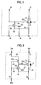
- Fig. 5 shows still another embodiment of a semiconductor device according to the invention.
- the same sections as those in Fig. 1 are given the same reference numerals .
- the source S2 of the second FET Q20 is isolated from the source S2 of the first FET Q1 and connected to an external terminal 29 provided separately from the external terminal 22.
- the sources S1 and S2 can be conducted electrically on the component side of a substrate.
- the first FET Q10 and the second FET Q20 may be arranged on a single chip or formed into separate chips. This embodiment also provides the same effects as the embodiment in Fig. 1 mentioned earlier.
- Fig. 6 shows still another embodiment of a semiconductor device according to the invention.
- the semiconductor device comprises a third FET Q30, by which the gate G1 of the first FET Q10 is driven.
- the first FET Q10 and the second FET 20 comprise n-channels and the third FET Q30 comprise a p-channel.
- a drain D3 of the third FET Q30 is connected to the external terminal 23.
- An operating voltage Vcc is supplied to the external terminal 23.
- a gate G3 of the third FET Q30 is, together with the gate G2 of the second FET Q20, connected to the external terminal 24. Further, a source S3 of the third FET Q30 is connected to the gate G1 of the first FET Q10.
- the first FET Q10, the second FET Q20 and the third FET Q30 may be arranged on a single chip or formed into separate chips.
- Fig. 7 shows a synchronous rectifier system step-down DC-to-DC converter using a semiconductor device shown in Figs. 1 through 4 as a commutation switch device 5.
- a DC voltage or a voltage Vin supplied from a DC power supply 41 to input terminals T11, T12 is switched using a control switch device Qm.
- a reference numeral 42 represents an input capacitor.
- the control switch device Qm is controlled by a control circuit 43.
- the control circuit 43 controls an output voltage Vo by adjusting the on period (duty ratio) of the control switch device Qm in the control operation.
- the output voltage Vo is supplied to a load 47 via output terminals T21, T22 connected at both ends of a capacitor 42.
- the commutation switch device 5 is turned on to continuously feed a current to an inductor 45.
- An idle period (dead time) is provided in which the control switch device Qm and the commutation switch device 5 are not turned on simultaneously in order to prevent occurrence of a through current. In this idle period, the current flowing across the inductor 45 flows in the diode 3 arranged in parallel with the commutation switch device 5.
- the on and off timings of the control switch device Qm and the commutation switch device 5 are controlled by the control circuit 43.
- the commutation switch device 5 is a semiconductor device according to the invention shown in Figs. 1 through 4 and has the drain D2 and the source S2 of the second FET Q20 connected to the gate G1 and the source S1 of the first FET Q10.
- the drive signal SG2 is supplied to the external terminal 24 to turn on the second FET Q20.
- This causes the second FET Q20 to short-circuit the gate G1 and the source S1 of the first FET Q10, thereby short-circuiting the gate-to-source capacitance Cgs of the first FET Q10 with low impedance.
- first FET Q10 and the second FET Q20 are in the same package 1 and the wiring impedance across the second FET Q20 and the first FET Q10 is remarkably low so that it is possible to decrease the gate-to-source voltage Vgs sufficiently below the threshold voltage. This reliably avoids the risk of the first FET Q10 that should be off entering the on state (self turn-on state).
- the package 1 comprises external terminals 21 through 24 on its outer surface.
- the drains D1, D2, sources S1, S2 and gates G1, G2 of the first and second FETs are connected to these terminals 21 through 24.
- the package 1 can be directly mounted on a circuit board as a single component.
- a semiconductor device shown in Figs. 4 through 6 can be used as the commutation switch device 5.
- a semiconductor device according to the invention can be used as a synchronous rectifying device of an output rectifier circuit in an isolated-type DC-to-DC converter equipped with a transformer for power conversion.
Landscapes
- Engineering & Computer Science (AREA)
- Power Engineering (AREA)
- Dc-Dc Converters (AREA)
- Semiconductor Integrated Circuits (AREA)
- Metal-Oxide And Bipolar Metal-Oxide Semiconductor Integrated Circuits (AREA)
- Rectifiers (AREA)
- Junction Field-Effect Transistors (AREA)
- Electronic Switches (AREA)
Abstract
Description
Claims (10)
- A semiconductor device comprising:wherein said external terminals are connected with the drains, sources or gates of said first and second field effect transistors.a first field effect transistor that composes a main switch;a second field effect transistor that has its drain and source connected to the gate and the source of said first field effect transistor; anda package having external terminals on its outer surface, in that said first field effect transistor and said second field effect transistor are placed,
- A semiconductor device according to claim 1, wherein said first and said second field effect transistors are formed in a single chip.
- A semiconductor device according to claim 1, wherein said first and said second field effect transistors are formed in separate chips.
- A semiconductor device according to claim 1, wherein said semiconductor device further comprises a third field effect transistor formed in said package, a source being connected to the gate of said first field effect transistor, agate is connected to said gate of said second field effect transistor, and a drain is connected to said external terminal.
- A semiconductor device according to any one of claims 1 through 4, wherein said semiconductor device is used as one of a switch device and a rectifying device.
- A DC-to-DC converter having a synchronous rectifier circuit wherein said synchronous rectifier circuit comprises a rectifying device includes a semiconductor device comprising:wherein said external terminals are connected with the drains, sources or gates of said first and second field effect transistors.a first field effect transistor that composes a main switch;a second field effect transistor that has its drain and source connected to the gate and the source of said first field effect transistor; anda package having external terminals on its outer surface, in that said first field effect transistor and said second field effect transistor are placed,
- A DC-to-DC converter according to claim 6, wherein said first and said second field effect transistors are formed in a single chip.
- A DC-to-DC converter according to claim 6, wherein said first and said second field effect transistors are formed in separate chips.
- A DC-to-DC converter according to claim 6, wherein said semiconductor device further comprises a third field effect transistor formed in said package, a source being connected to the gate of said first field effect transistor, a gate is connected to said gate of said second field effect transistor, and a drain is connected to said external terminal.
- A DC-to-DC converter according to any one of claims 6 through 9, wherein said semiconductor device is used as one of a switch device and a rectifying device.
Applications Claiming Priority (2)
| Application Number | Priority Date | Filing Date | Title |
|---|---|---|---|
| JP2001085622 | 2001-03-23 | ||
| JP2001085622A JP2002290224A (en) | 2001-03-23 | 2001-03-23 | Semiconductor element |
Publications (2)
| Publication Number | Publication Date |
|---|---|
| EP1244202A2 true EP1244202A2 (en) | 2002-09-25 |
| EP1244202A3 EP1244202A3 (en) | 2003-05-28 |
Family
ID=18941103
Family Applications (1)
| Application Number | Title | Priority Date | Filing Date |
|---|---|---|---|
| EP02006404A Withdrawn EP1244202A3 (en) | 2001-03-23 | 2002-03-21 | Semiconductor device |
Country Status (4)
| Country | Link |
|---|---|
| US (1) | US20020134999A1 (en) |
| EP (1) | EP1244202A3 (en) |
| JP (1) | JP2002290224A (en) |
| CN (1) | CN1378285A (en) |
Cited By (2)
| Publication number | Priority date | Publication date | Assignee | Title |
|---|---|---|---|---|
| EP1594164B1 (en) * | 2003-02-14 | 2012-05-09 | Hitachi, Ltd. | Integrated circuit for driving semiconductor device |
| EP2779453A1 (en) * | 2013-03-11 | 2014-09-17 | Semiconductor Components Industries, LLC | Circuit including a Switching Element, a Rectifying Element, and a Charge Storage Element |
Families Citing this family (18)
| Publication number | Priority date | Publication date | Assignee | Title |
|---|---|---|---|---|
| JP2004112987A (en) * | 2002-07-26 | 2004-04-08 | Fuji Electric Holdings Co Ltd | Power converter |
| JP4477952B2 (en) * | 2004-07-09 | 2010-06-09 | 株式会社ルネサステクノロジ | Semiconductor device, DC / DC converter and power supply system |
| EP1844461A4 (en) * | 2005-01-24 | 2009-05-27 | Ifire Ip Corp | PILOT OF COLUMNS WITH LOW ENERGY CONSUMPTION FOR ELECTROLUMINESCENT DISPLAYS |
| JP4739059B2 (en) | 2006-02-23 | 2011-08-03 | ルネサスエレクトロニクス株式会社 | Semiconductor device for DC / DC converter |
| US7929321B2 (en) * | 2008-08-22 | 2011-04-19 | Force-Mos Technology Corp | Depletion mode trench MOSFET for improved efficiency of DC/DC converter applications |
| US8294371B2 (en) | 2009-08-17 | 2012-10-23 | GE Lighting Solutions, LLC | LED traffic signal with synchronized power pulse circuit |
| EP2517341B1 (en) * | 2009-12-23 | 2019-06-26 | Marvell World Trade Ltd. | Start-up supply for a switch mode power supply |
| US20110148376A1 (en) * | 2009-12-23 | 2011-06-23 | Texas Instruments Incorporated | Mosfet with gate pull-down |
| JP5285103B2 (en) | 2011-03-10 | 2013-09-11 | 株式会社東芝 | Nitride semiconductor device |
| JP2012199763A (en) * | 2011-03-22 | 2012-10-18 | Sanken Electric Co Ltd | Gate drive circuit |
| JP5766992B2 (en) * | 2011-03-24 | 2015-08-19 | トランスフォーム・ジャパン株式会社 | Switching circuit device |
| CN103534915B (en) * | 2011-05-16 | 2016-08-17 | 马维尔国际贸易有限公司 | High-voltage starting circuit |
| JP5482815B2 (en) * | 2011-06-01 | 2014-05-07 | 株式会社デンソー | Power MOSFET drive circuit and element value determination method thereof |
| JP5961944B2 (en) * | 2011-08-18 | 2016-08-03 | サンケン電気株式会社 | Gate drive circuit |
| JP6171451B2 (en) * | 2013-03-25 | 2017-08-02 | セイコーエプソン株式会社 | Circuit device and electronic device |
| CN106549568B (en) * | 2016-12-09 | 2019-07-09 | 芯洲科技(北京)有限公司 | A kind of switching device driving circuit, method and boostrap circuit |
| GB2590057B (en) * | 2019-10-10 | 2022-11-16 | Steifpower Tech Company Limited | A Field-Effect Transistor (FET) based synchronous rectifier for emulating a diode |
| CN115267476B (en) * | 2022-07-28 | 2025-03-21 | 上海华虹宏力半导体制造有限公司 | Measuring device and method for gate series resistance small pad device |
Family Cites Families (5)
| Publication number | Priority date | Publication date | Assignee | Title |
|---|---|---|---|---|
| US5006736A (en) * | 1989-06-13 | 1991-04-09 | Motorola, Inc. | Control circuit for rapid gate discharge |
| US5206544A (en) * | 1991-04-08 | 1993-04-27 | International Business Machines Corporation | CMOS off-chip driver with reduced signal swing and reduced power supply disturbance |
| JP2956319B2 (en) * | 1991-11-07 | 1999-10-04 | 富士電機株式会社 | Reverse bias control circuit for voltage driven switching element |
| JP3222330B2 (en) * | 1994-09-20 | 2001-10-29 | 株式会社日立製作所 | Semiconductor circuit and semiconductor integrated circuit |
| US6111769A (en) * | 1999-09-24 | 2000-08-29 | Ericsson, Inc. | External driving circuit for bridge type synchronous rectification |
-
2001
- 2001-03-23 JP JP2001085622A patent/JP2002290224A/en not_active Withdrawn
-
2002
- 2002-03-21 EP EP02006404A patent/EP1244202A3/en not_active Withdrawn
- 2002-03-22 CN CN02108203.0A patent/CN1378285A/en active Pending
- 2002-03-22 US US10/102,828 patent/US20020134999A1/en not_active Abandoned
Cited By (3)
| Publication number | Priority date | Publication date | Assignee | Title |
|---|---|---|---|---|
| EP1594164B1 (en) * | 2003-02-14 | 2012-05-09 | Hitachi, Ltd. | Integrated circuit for driving semiconductor device |
| EP2779453A1 (en) * | 2013-03-11 | 2014-09-17 | Semiconductor Components Industries, LLC | Circuit including a Switching Element, a Rectifying Element, and a Charge Storage Element |
| US9070562B2 (en) | 2013-03-11 | 2015-06-30 | Semiconductor Components Industries, Llc | Circuit including a switching element, a rectifying element, and a charge storage element |
Also Published As
| Publication number | Publication date |
|---|---|
| CN1378285A (en) | 2002-11-06 |
| US20020134999A1 (en) | 2002-09-26 |
| JP2002290224A (en) | 2002-10-04 |
| EP1244202A3 (en) | 2003-05-28 |
Similar Documents
| Publication | Publication Date | Title |
|---|---|---|
| US20020134999A1 (en) | Semiconductor device | |
| EP1360763B1 (en) | Integrated fet and driver | |
| US6674268B2 (en) | Swithing regulator utilizing seperate integrated circuits for driving each switch | |
| US8018255B2 (en) | DC-DC converter, driver IC, and system in package | |
| US7157959B2 (en) | Method of forming a self-gated transistor and structure therefor | |
| US8547162B2 (en) | Integration of MOSFETs in a source-down configuration | |
| US6617642B1 (en) | Field effect transistor structure for driving inductive loads | |
| US8637909B1 (en) | Mixed mode dual switch | |
| US8148957B2 (en) | Power switch-mode circuit with devices of different threshold voltages | |
| US7838901B2 (en) | Single-chip common-drain JFET device and its applications | |
| JP2011152011A (en) | Semiconductor device and power supply unit using the same | |
| US20030111983A1 (en) | Efficient buck topology DC-DC power stage utilizing monolithic N- channel upper FET and pilot current sensing | |
| WO2019113220A1 (en) | Power unit with an integrated pull-down transistor | |
| JP2010136620A (en) | Semiconductor apparatus | |
| US7265525B2 (en) | Self-driven scheme for synchronous rectifier having no body diode | |
| AU2004216021A1 (en) | On chip power supply | |
| US20250350279A1 (en) | High Voltage Converter Power Stage | |
| US7439771B2 (en) | Integrated interface circuitry for integrated VRM power field effect transistors | |
| US20240355717A1 (en) | Integrated bidirectional four quadrant switches with drivers and input/output circuits | |
| JP2018152781A (en) | Surge suppression circuit | |
| WO1997045957A1 (en) | Semiconductor device | |
| KR20020093021A (en) | Switching fet circuit | |
| JP2002100970A (en) | Switching circuit | |
| JPWO1997044884A1 (en) | Switching power supply circuit |
Legal Events
| Date | Code | Title | Description |
|---|---|---|---|
| PUAI | Public reference made under article 153(3) epc to a published international application that has entered the european phase |
Free format text: ORIGINAL CODE: 0009012 |
|
| AK | Designated contracting states |
Kind code of ref document: A2 Designated state(s): AT BE CH CY DE DK ES FI FR GB GR IE IT LI LU MC NL PT SE TR |
|
| AX | Request for extension of the european patent |
Free format text: AL;LT;LV;MK;RO;SI |
|
| PUAL | Search report despatched |
Free format text: ORIGINAL CODE: 0009013 |
|
| AK | Designated contracting states |
Designated state(s): AT BE CH CY DE DK ES FI FR GB GR IE IT LI LU MC NL PT SE TR |
|
| AX | Request for extension of the european patent |
Extension state: AL LT LV MK RO SI |
|
| AKX | Designation fees paid | ||
| REG | Reference to a national code |
Ref country code: DE Ref legal event code: 8566 |
|
| STAA | Information on the status of an ep patent application or granted ep patent |
Free format text: STATUS: THE APPLICATION IS DEEMED TO BE WITHDRAWN |
|
| 18D | Application deemed to be withdrawn |
Effective date: 20031129 |