EP1244148A2 - Semiconductor memory - Google Patents
Semiconductor memory Download PDFInfo
- Publication number
- EP1244148A2 EP1244148A2 EP02250261A EP02250261A EP1244148A2 EP 1244148 A2 EP1244148 A2 EP 1244148A2 EP 02250261 A EP02250261 A EP 02250261A EP 02250261 A EP02250261 A EP 02250261A EP 1244148 A2 EP1244148 A2 EP 1244148A2
- Authority
- EP
- European Patent Office
- Prior art keywords
- transistor
- rows
- memory cell
- transistors
- memory
- Prior art date
- Legal status (The legal status is an assumption and is not a legal conclusion. Google has not performed a legal analysis and makes no representation as to the accuracy of the status listed.)
- Withdrawn
Links
Images




Classifications
-
- H—ELECTRICITY
- H10—SEMICONDUCTOR DEVICES; ELECTRIC SOLID-STATE DEVICES NOT OTHERWISE PROVIDED FOR
- H10B—ELECTRONIC MEMORY DEVICES
- H10B69/00—Erasable-and-programmable ROM [EPROM] devices not provided for in groups H10B41/00 - H10B63/00, e.g. ultraviolet erasable-and-programmable ROM [UVEPROM] devices
-
- G—PHYSICS
- G11—INFORMATION STORAGE
- G11C—STATIC STORES
- G11C16/00—Erasable programmable read-only memories
- G11C16/02—Erasable programmable read-only memories electrically programmable
- G11C16/06—Auxiliary circuits, e.g. for writing into memory
-
- G—PHYSICS
- G11—INFORMATION STORAGE
- G11C—STATIC STORES
- G11C16/00—Erasable programmable read-only memories
- G11C16/02—Erasable programmable read-only memories electrically programmable
- G11C16/04—Erasable programmable read-only memories electrically programmable using variable threshold transistors, e.g. FAMOS
- G11C16/0483—Erasable programmable read-only memories electrically programmable using variable threshold transistors, e.g. FAMOS comprising cells having several storage transistors connected in series
-
- H—ELECTRICITY
- H10—SEMICONDUCTOR DEVICES; ELECTRIC SOLID-STATE DEVICES NOT OTHERWISE PROVIDED FOR
- H10B—ELECTRONIC MEMORY DEVICES
- H10B41/00—Electrically erasable-and-programmable ROM [EEPROM] devices comprising floating gates
- H10B41/10—Electrically erasable-and-programmable ROM [EEPROM] devices comprising floating gates characterised by the top-view layout
-
- H—ELECTRICITY
- H10—SEMICONDUCTOR DEVICES; ELECTRIC SOLID-STATE DEVICES NOT OTHERWISE PROVIDED FOR
- H10B—ELECTRONIC MEMORY DEVICES
- H10B41/00—Electrically erasable-and-programmable ROM [EEPROM] devices comprising floating gates
- H10B41/30—Electrically erasable-and-programmable ROM [EEPROM] devices comprising floating gates characterised by the memory core region
Definitions
- the present invention relates to the layout of a memory cell array in a semiconductor memory, and more particularly to a technology for reducing the chip size of a semiconductor memory.
- Nonvolatile semiconductor memories such as a flash memory have voltage generators for supplying a high voltage or a low voltage to source lines according to memory operations.
- United States Patent Application No. 5,293,350 has disclosed a technique in which a sense amplifier, a voltage generator, and the like are shared among a plurality of bit lines and the like, to reduce the chip size of the semiconductor memory.
- Figs. 1 A and 1 B show the essential parts of a semiconductor memory of this type.
- Fig. 1A shows the circuit configuration and
- Fig. 1B shows a sectional structure of the area that is shown by the broken lines in Fig. 1A.
- a memory cell array 1 is provided with bit lines BL0 and BL1, which are connected to its memory cells (not shown).
- the bit lines BL0 and BL1 are connected to a sense amplifier 3 (or a voltage generator etc.) through transistors 2a and 2b respectively and a common signal line CMN.
- the gates of the transistors 2a and 2b are connected to control lines 4a and 4b respectively.
- the control lines 4a and 4b are laid perpendicular to the bit lines BL0 and BL1.
- one of the control lines 4a and 4b is changed to a high level, turning ON either of the transistors 2a and 2b. It follows that one of the bit lines BL0 and BL1 is connected to the sense amplifier 3 through the common signal line CMN, whereby the data read out from a memory cell to the bit line BL0 (or BL1) is amplified. That is, the sense amplifier 3 is shared between the bit lines BL0 and BL1.
- the transistor 2a is composed of diffusion layers (a source S and a drain D) which are formed in a semiconductor substrate SUB, and a control line 4a which is laid on the semiconductor substrate SUB via a gate insulator.
- the source S of the transistor 2a is connected to the common signal line CMN.
- the drain D of the transistor is connected to the bit line BL0. Since the broken-lined area of Fig. 1A allows no transistor that has the control line 4b as its gate, the source and the drain (diffusion layers) corresponding to the control line 4b are not formed in the semiconductor substrate SUB.
- Fig. 2 shows an overview of the fabrication process for forming the source S and the drain D of the transistor 2a.
- the source S and the drain D are formed by implanting ions into the semiconductor substrate SUB with the gate of the transistor 2a (the control line 4a) as a mask.
- a photoresist 5 is initially applied to over the semiconductor substrate SUB (wafer) and then baked. Next, exposure is performed using a photomask 6, followed by development, so that the photoresist 5 is processed into a shape corresponding to the photomask 6 as shown in Fig. 2. Subsequently, as shown by the arrows in the diagram, phosphorus or other ions are implanted selectively to form the source S and the drain D of the transistor 2a.
- the control lines 4a and 4b to be the gates of the transistors 2a and 2b are laid perpendicular to the bit lines BL0 and BL1.
- the transistors 2a and 2b are formed by implanting ions with these control lines 4a and 4b as masks. This requires that regions undesired of transistor formation (for example, the regions adjacent to the control line 4b within the broken-lined area of Fig. 1A) must be masked with the photoresist 6. In other words, to selectively connect the bit lines BL0 and BL1 to the sense amplifier 3 and the like, the photoresist 6 needs to be opened for each of the transistors 2a and 2b corresponding to the bit lines BL0 and BL1, respectively.
- the openings in the photoresist 6 must be made with predetermined margins from the regions to form transistors and those not to form transistors. Owing to these margins, there has been a problem of an increased layout area when the wiring spacing between the control lines 4a and 4b needs to be extended beyond the formable minimum process size. Since the increased layout area grows the chip size of the semiconductor memory, there has been a problem of a rise in product costs.
- the memory cell array and its peripheral regions contain a number of identical circuits arranged repeatedly. On this account, an increase in the layout area of these regions has a significant impact on the product costs of the semiconductor memory.
- a semiconductor memory has a plurality of memory cell rows, an input/output circuit for inputting/outputting data to/from the memory cell rows, and a plurality of first transistor rows arranged for each of the memory cell rows.
- the memory cell rows include a plurality of memory cells connected in series.
- the memory cells may be nonvolatile memory cells each having a control gate and a floating gate, and the memory cell rows are configured as a NAND type.
- the first transistor rows have a plurality of transistors connected in series.
- the memory cell rows may be connected to the first transistor rows through local bit lines, respectively.
- the first transistor rows may be connected to the input/output circuit through a global bit line, which is common to these transistor rows.
- a switching transistor operates as a switch while a short transistor(s) each having a source and a drain shorted to each other function(s) as wiring.
- any of the switches (transistors) among the plurality of first transistor rows turns on to selectively connect any of the memory cell rows to the input/output circuit. That is, the input/output circuit is shared among the plurality of memory cell rows.
- the first transistor rows are provided with the plurality of transistors in advance regardless of whether or not to use the transistors as switches. Since there is no need to selectively form only such a transistor that is to be operated as a switch, there is no need to form ion-implanted regions for making a source and a drain per transistor. As a result, the pattern shape of the photomask corresponding to the ion-implanted regions (the layout rule of the diffusion layer regions) need not be taken account of when arranging the spacing between the transistors of the first transistor rows (the wiring spacing of the gate material). Since the transistors can be arranged closely, the layout area of the first transistor rows can be reduced. This allows a reduction in the chip size of the semiconductor memory.
- the present invention offers a high effect when applied to nonvolatile semiconductor memories of NAND type which feature high integration.
- the semiconductor memory is preferably provided with a plurality of the memory cell rows corresponding to each of the first transistor rows. These memory cell rows are respectively connected to a corresponding transistor row of the first transistor rows through selecting transistors in each of the memory cell rows. Since any of the memory cell rows can be selectively connected to the corresponding transistor row of the first transistor rows by the selecting transistors, the first transistor rows can be shared among a plurality of memory cell rows. As a result, the input/output circuit can be shared among a greater number of memory cell rows and the chip size can be reduced.
- the source and the drain of the short transistor not to be operated as a switch are preferably shorted to each other by using metal wiring.
- the metal wiring may be formed in a latter stage of the semiconductor fabrication processes after the formation of the transistors of the transistor rows. Therefore, for example, when prototyping the semiconductor memory, even if a mistake is found in a position of the transistor to be operated as a switch in each of the first transistor rows, this mistake can be corrected by simply changing the photomask in the wiring process. Conventionally, when such mistake is found, a makeover from the process of forming the diffusion layers (the source and the drain of the transistor) was needed.
- the semiconductor memory preferably has a voltage generator for supplying a predetermined voltage to the unselected memory cell row(s) among the memory cell rows, and a plurality of second transistor rows arranged for each of the memory cell rows.
- the second transistor rows include a plurality of transistors connected in series.
- the memory cell rows may be connected to the first and second transistor rows through local bit lines, and the second transistor rows are connected to the voltage generator through a bit control line, which is common to these transistor rows.
- a switching transistor operates as a switch while a short transistor(s) each having a source and a drain shorted to each other function(s) as wiring.
- any of the switches (transistors) among the plurality of second transistor rows turn(s) on to selectively connect any of the memory cell rows to the voltage generator. That is, the voltage generator is shared among the plurality of memory cell rows.
- the voltage generator supplies, for example, a first voltage and a second voltage to the local bit line(s) of the unselected memory cell row(s), respectively, when the selected memory cell row among the memory cell rows performs a read operation and a write operation.
- the second transistor rows are provided with the plurality of transistors in advance. Since there is no need to selectively form only such a transistor that is to be operated as a switch, there is no need to form ion-implanted regions for making a source and a drain per transistor. As a result, the pattern shape of the photomask corresponding to the ion-implanted regions (the layout rule of the diffusion layer regions) need not be taken account of when arranging the spacing between the transistors of the second transistor rows (the wiring spacing of the gate material). Since the transistors can be arranged closely, the layout area of the second transistor rows can be reduced. This allows a reduction in the chip size of the semiconductor memory.
- the input/output circuit and the voltage generator are preferably arranged on both sides of the memory cell rows. On this account, the input/output circuit and the voltage generator can be efficiently arranged in the peripheral regions of the memory cell rows without increasing the layout area.
- the source and the drain of the short transistor not to be operated as a switch are preferably shorted to each other by using metal wiring.
- the metal wiring may be formed in a latter stage of the semiconductor fabrication processes after the formation of the transistors of the transistor rows. Therefore, for example, when prototyping the semiconductor memory, even if a mistake is found in position of the transistor to be operated as a switch in each of the second transistor rows, this mistake can be corrected by simply changing the photomask in the wiring process.
- Fig. 3 shows an embodiment of the semiconductor memory in the present invention.
- This semiconductor memory is formed as a flash memory (nonvolatile semiconductor memory) of NAND type on a silicon substrate by using CMOS processes.
- the flash memory has an input/output unit 10 for inputting/outputting commands, addresses, data, and the like, a control unit 12 for controlling read operations, write operations (program operations), and erase operations, and a memory array unit 14 including memory cell arrays and peripheral circuits thereof.
- the memory array unit 14 is divided into a plurality of memory cores M.
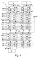
- Fig. 4 shows part of the memory cores M.
- a memory core M has a memory cell array MA, along with input/output circuits 16, a voltage generator 18, an address decoder, etc. (not shown) which are arranged around this memory cell array MA.
- the input/output circuits 16 include sense amplifiers, write amplifiers, and so on.
- the input/output circuits 16 and the voltage generator 18 are arranged on both sides of the memory cell array MA. This allows the input/output circuits and the voltage generator to be efficiently arranged in the peripheral regions of the memory cell array MA without increasing the layout area of the memory core M.
- the memory cell array MA has a plurality of memory cell rows MR, a plurality of first transistor rows TR1, and a plurality of second transistor rows TR2.
- the plurality of memory cell rows MR is arranged in series along local bit lines LBL0, LBL1, LBL2, LBL3, ... which are laid vertically in the diagram.
- the first transistor rows TR1 are arranged on an end of the memory cell array MA closer to the input/output circuits 16.
- the second transistor rows TR2 are arranged on an end of the memory cell array MA closer to the voltage generator 18.
- Each memory cell row MR has sixteen memory cells 20 connected in series and two selecting transistors 22a, 22b.
- Each of the memory cells 20 has a control gate and a floating gate.
- the gates of the memory cells 20 each are connected to one of word lines WL0-WL15.
- the gates of the selecting transistors 22a and 22b are connected to selecting lines SG1 and SG2, respectively.
- the source and the drain of the selecting transistor 22a are connected to the memory cell 20 that is controlled by the word line WL0 and to the local bit line LBL0 (or LBL1, LBL2, LBL3), respectively.
- the source and the drain of the selecting transistor 22b are connected to the memory cell 20 that is controlled by the word line WL15 and to a source line ARVSS, respectively.
- the source line ARVSS is a common power supply line connected to all the selecting transistors 22b in the memory cell array MR.
- the source line ARVSS becomes 0 V in read operations, becomes 4 V in write operations, and becomes floating in erase operations.
- Each of the first transistor rows TR1 has two transistors 24a and 24b (a switching transistor or a short transistor) connected in series.
- Each first transistor row TR1 is connected to the local bit line LBL0 (or LBL1, LBL2, LBL3) and a global bit line GBL0 (or GBL1) at one end and at the other end, respectively.
- the gates of the transistors 24a and 24b are connected to selecting lines PS0 and PS1, respectively.
- the voltages of the selecting lines PS0 and PS1 are set in accordance with an address signal supplied from the exterior of the memory.
- the transistors 24b short transistors
- the transistors 24a short transistors
- the transistors 24a have their source and drain shorted with aluminum wiring or the like so as to function as wiring.
- the second transistor rows TR2 each have two transistors 26a and 26b (a switching transistor or a short transistor) connected in series. Each second transistor row TR2 is connected at one end and at the other end to the local bit line LBL0 (or LBL1, LBL2, LBL3) and a bit control line BLCOM, respectively. The gates of the transistors 26a and 26b are connected to the selecting lines PS0 and PS1, respectively.
- the transistors 26a short transistors
- the transistors 26a have their source and drain shorted with aluminum wiring or the like so as to be masked of transistor functions. That is, these transistors function as wiring.
- the transistors 26b short transistors
- the transistors 26b have their source and drain shorted with aluminum wiring or the like so as to function as wiring.
- this embodiment is characterized in that a plurality of transistors connected in series (first transistor row TR1) are arranged between the local bit line LBL0 (or LBL1, LBL2, LBL3) and the global bit line GBL0 (or GBL1).
- first transistor row TR1 a plurality of transistors connected in series
- second transistor row TR2 are arranged between the local bit line LBL0 (or LBL1, LBL2, LBL3) and the bit control line BLCOM.
- the input/output circuits 16 are formed corresponding to the global bit lines GBL0 and GBL1, respectively.
- the input/output circuits 16 input/output data to be read/written from/to the memory cell rows MR through the global bit line GBL0 (or GBL1).
- the voltage generator 18 is formed, for example, one for each memory core M.
- the voltage generator 18 supplies a predetermined voltage to the local bit lines LBL of memory cell rows MR that are not in operation. More specifically, the voltage generator 18 outputs 0 V in read operations, outputs 4 V in write operations, and suspends output in erase operations (floating).
- Fig. 5 shows the layout of the memory core M shown in Fig 4.
- the selecting lines PS0, PS1, selecting lines SG1, SG2, and word lines WL0-WL15 shown shaded (extending horizontally in the diagram) are made of gate material such as polysilicon.
- the global bit lines GBL0, GBL1, local bit lines LBL0, LBL1, LBL2, LBL3, and bit control line BLCOM shown in full lines (extending vertically in the diagram) are made of metal such as aluminum.
- the broken-lined area indicates diffusion layers (the sources and the drains of the transistors, and wiring). More specifically, in the forming process of the diffusion layers, an opening is made in the photoresist within the broken-lined area (on the side including contact holes, which are shown by the squares). Phosphorous or other ions are implanted to inside this area with gate wiring as a mask. Therefore, the diffusion layers are formed within the area exclusive of where the polysilicons lie, which are shown shaded.
- all the first and second transistor rows TR1 and TR2 are provided with the transistors that have the selecting lines PS0 and PS1 as their gates. That is, the transistor rows TR1 and TR2 are provided with two transistors each. As described in Fig. 4, in the first transistor rows TR1 connected with the even-numbered local bit lines LBL0 and LBL2, the sources and the drains of the transistors that have the selecting line PS1 as their gates are connected to each other by aluminum wiring or the like through the contact holes. In the second transistor rows TR2 connected with the even-numbered local bit lines LBL0 and LBL2, the sources and the drains of the transistors that have the selecting line PS0 as their gates are connected to each other by aluminum wiring or the like through the contact holes.
- the sources and the drains of the transistors that have the selecting line PS0 as their gates are connected to each other by aluminum wiring or the like through the contact holes.
- the sources and the drains of the transistors that have the selecting line PS1 as their gates are connected to each other by aluminum wiring or the like through the contact holes.
- the opening of the photoresist (forming area of the diffusion layers) is not made in units of transistors but formed into an area extending along the local bit lines LBL0-LBL3. This makes it possible to minimize the wiring spacing between the selecting lines PS0 and PS1 independent of the layout rule of the photoresist openings. Consequently, the memory cores M become smaller in layout size as compared to heretofore.
- the connections between the sources and the drains of the transistor rows TR1, TR2 are established by aluminum wiring. Therefore, even if mistakes are found in the prototyping or other phases of the flash memory as to the positions of transistors to be masked of functions in the transistor rows, the mistakes can be dealt with merely by making over the photomask for the wiring process using aluminum or the like. That is, prototyping defects can be fed back promptly and easily. Conventionally, mistakes of transistor positions necessitated a makeover from the diffusion process, taking much time for the defects to be fed back.
- Fig. 6 shows a section of the first transistor row TR1 connected to the local bit line LBL0.
- the first transistor row TR1 has the two transistors 24a and 24b.
- the source S of the transistor 24a is connected to the global bit line GBL0.
- the drain D of the transistor 24a is connected to the local bit line LBL0.
- Both the source S and the drain D of the transistor 24b are connected to the local bit line LBL0 through aluminum wiring. Accordingly, the transistor 24b, though formed as a device, is masked of transistor functions.
- the drain D of the transistor 24a and the source S of the transistor 24b are an identical diffusion layer since the transistors 24a and 24b are connected in series.
- FIG. 4 an overview will be given of a read operation, a write operation, and an erase operation of the flash memory in the present embodiment.
- a word line (WL1, for example) connected to a memory cell 20 to read data from is supplied with 0V, and the other word lines (WL0 and WL2-WL15, for example) are supplied with 4V.
- the source line ARVSS is supplied with 0V.
- a word line (WL1, for example) connected to a memory cell 20 to write data to is supplied with 20V, and the other word lines (WL0 and WL2-WL15, for example) are supplied with 10V.
- the source line ARVSS is supplied with 4 V. Then, electrons are tunnel-injected to the floating gate of the memory cell 20 to write data to, so that the threshold voltage of the memory cell 20 rises for data write.
- all the word lines WL0-WL15 are supplied with 0V, and the source line ARVSS is brought into a floating state. Then, the well region of the memory core M is supplied with 20V so that electrons trapped in the floating gates are emitted into the well region. Then, the threshold voltages of the memory cells 20 drop for data erase. The erase operation is performed on all the memory cells 20 in the memory core M.
- the address decoder operates to turn the selecting lines PS0 and PS1 to a high level and a low level, respectively.
- the transistor 24a turns ON in response to the high level of the selecting line PS0. Since the transistor 24b is shorted between its source and drain, the turning-ON of the transistor 24a connects the local bit line LBL0 to the input/output circuit 16 through the global bit line GBL0.
- the transistor 24b turns OFF in response to the low level of the selecting line PS1. Therefore, the local bit line LBL1 is not connected to the input/output circuit 16.
- the transistor 26b turns OFF in response to the low level of the selecting line PS1. Therefore, the local bit line LBL0 is not connected to the voltage generator 18.
- the transistor 26a turns ON in response to the high level of the selecting line PS0. Since the transistor 26b is shorted between its source and drain, the turning-ON of the transistor 26a connects the local bit line LBL1 to the voltage generator 18 through the bit control line BLCOM. The voltage generator 18 supplies 0V to the local bit line LBL1.
- the memory cell rows MR connected with the local bit line LBL1 are supplied with 0V at both ends, thereby being inactivated. Then, the memory cell rows MR connected with the local bit line LBL0 perform a read operation or a write operation as described above.
- both the selecting lines PS0 and PS1 are turned to the low level. All the local bit lines LBL0-LBL3 enter the floating state, and the erase operation is performed as described above.
- Fig. 7 shows the circuit of a memory core M, which has been studied by the present inventors before the achievement of the present invention.
- bit lines BL0, BL1, BL2, and BL3 are provided with an input/output circuits 16 each.
- a plurality of memory cell rows MR is connected at one end to the bit lines BL0, BL1, BL2, and BL3, respectively.
- the other ends of the memory cell rows MR are connected to a common source line ARVSS.
- the first transistor rows TR1 are provided with a plurality of transistors 24a and 24b in advance.
- either of the transistors is shorted between its source and drain so that one of the transistors 24a and 24b operates as a switch and the other transistor functions as wiring.
- the second transistor rows TR2 are provided with a plurality of transistors 26a and 26b in advance.
- either of the transistors is shorted between its source and drain so that one of the transistors 26a and 26b operates as a switch and the other transistor functions as wiring. This eliminates the need for forming ion-implanted regions for making the source and the drain per transistor.
- the present invention offers a high effect when applied to nonvolatile semiconductor memories of NAND type which feature high integration.
- a plurality of memory cell rows MR is arranged in series corresponding to the first transistor rows TR1. Sharing the first transistor rows TR1 among a plurality of memory cell rows MR allows the input/output circuit 18 to be shared among a greater number of memory cell rows MR, with a reduction in chip size.
- the transistors 24a, 24b, 26a, and 26b not to be operated as switches are shorted between their source and drain by using aluminum wiring. On this account, even if a mistake is found in the positions of transistors to be operated as switches, this mistake can be corrected by simply changing the photomask in the wiring process.
- the input/output circuits 16 and the voltage generator 18 are arranged on both sides of the memory cell rows MR. Therefore, these circuits 16 and 18 can be efficiently arranged in the peripheral regions of the memory cell rows without increasing the layout area.
- the foregoing embodiment has dealt with the case where the present invention is applied to a flash memory.
- the present invention is not limited to such an embodiment.
- the present invention may be applied to other nonvolatile semiconductor memories of NAND type.
- the foregoing embodiment has dealt with the case where the two local bit lines LBL0 and LBL1 are connected to the single global bit line GBL0.
- the present invention is not limited to such an embodiment.
- three or more local bit lines may be connected to a single global bit line.
- the input/output circuits 16 and the voltage generator 18 can be shared easily by making the numbers of transistors to be formed in the first and second transistor rows TR1 and TR2 identical to the number of local bit lines connected to the global bit line.
Landscapes
- Engineering & Computer Science (AREA)
- Microelectronics & Electronic Packaging (AREA)
- Semiconductor Memories (AREA)
- Read Only Memory (AREA)
- Non-Volatile Memory (AREA)
Abstract
Description
Claims (10)
- A semiconductor memory comprising:a plurality of memory cell rows each having memory cells connected in series;an input/output circuit for inputting/outputting data to/from said memory cell rows; anda plurality of first transistor rows corresponding to each of said memory cell rows for selectively connecting any of said memory cell rows to said input/output circuit, said first transistor rows each including a switching transistor operating as a switch and a short transistor(s) each having a source and a drain shorted to each other, which are connected in series.
- The semiconductor memory according to claim 1, comprising:local bit lines for connecting said memory cell rows to said first transistor rows, respectively; anda global bit line for connecting said first transistor rows to said input/output circuit.
- The semiconductor memory according to claim 1 or 2, comprising:a plurality of said memory cell rows corresponding to each of said first transistor rows; andselecting transistors in each of said memory cell rows for selectively connecting any of said memory cell rows to a corresponding transistor row of said first transistor rows.
- The semiconductor memory according to claim 1, 2 or 3, wherein
said source and said drain of said short transistor in each of said first transistor rows are shorted by metal wiring. - The semiconductor memory according to any preceding claim, comprising:a voltage generator for supplying a predetermined voltage to the unselected memory cell row(s) among said memory cell rows; anda plurality of second transistor rows corresponding to each of said memory cell rows for selectively connecting said unselected memory cell row(s) to said voltage generator, said second transistor rows each including a switching transistor operating as a switch and a short transistor(s) each having a source and a drain shorted to each other, which are connected in series.
- The semiconductor memory according to claim 5, comprising:local bit lines for connecting said memory cell rows to said first and second transistor rows, respectively; anda common bit control line for connecting said second transistor rows to said voltage generator.
- The semiconductor memory according to claim 6, wherein
said voltage generator supplies a first voltage and a second voltage to said local bit line(s) of said unselected memory cell row(s), respectively, when the selected memory cell row among said memory cell rows performs a read operation and a write operation. - The semiconductor memory according to claim 5, 6 or 7, wherein
said input/output circuit and said voltage generator are arranged on both sides of said memory cell rows. - The semiconductor memory according to any one of claims 5 to 8, wherein
said source and said drain of said short transistor in each of said second transistor rows are shorted by metal wiring. - The semiconductor memory according to any preceding claim, wherein:said memory cells are nonvolatile memory cells each having a control gate and a floating gate; andsaid memory cell rows are of NAND type.
Applications Claiming Priority (2)
| Application Number | Priority Date | Filing Date | Title |
|---|---|---|---|
| JP2001085532 | 2001-03-23 | ||
| JP2001085532A JP2002289705A (en) | 2001-03-23 | 2001-03-23 | Semiconductor memory |
Publications (2)
| Publication Number | Publication Date |
|---|---|
| EP1244148A2 true EP1244148A2 (en) | 2002-09-25 |
| EP1244148A3 EP1244148A3 (en) | 2007-01-03 |
Family
ID=18941027
Family Applications (1)
| Application Number | Title | Priority Date | Filing Date |
|---|---|---|---|
| EP02250261A Withdrawn EP1244148A3 (en) | 2001-03-23 | 2002-01-15 | Semiconductor memory |
Country Status (5)
| Country | Link |
|---|---|
| US (1) | US6507515B2 (en) |
| EP (1) | EP1244148A3 (en) |
| JP (1) | JP2002289705A (en) |
| KR (1) | KR100666017B1 (en) |
| TW (1) | TW520565B (en) |
Families Citing this family (8)
| Publication number | Priority date | Publication date | Assignee | Title |
|---|---|---|---|---|
| JP3659205B2 (en) * | 2001-08-30 | 2005-06-15 | セイコーエプソン株式会社 | Nonvolatile semiconductor memory device and driving method thereof |
| US6795326B2 (en) * | 2001-12-12 | 2004-09-21 | Micron Technology, Inc. | Flash array implementation with local and global bit lines |
| US7062738B1 (en) * | 2002-07-25 | 2006-06-13 | Taiwan Semiconductor Manufacturing Company | Flash memory compiler with flexible configurations |
| US7313023B2 (en) * | 2005-03-11 | 2007-12-25 | Sandisk Corporation | Partition of non-volatile memory array to reduce bit line capacitance |
| KR100746292B1 (en) | 2006-07-04 | 2007-08-03 | 삼성전자주식회사 | Nonvolatile memory device |
| US7889582B1 (en) | 2008-03-12 | 2011-02-15 | Netlogic Microsystems, Inc. | Segmented write bitline system and method |
| US8482981B2 (en) * | 2008-05-30 | 2013-07-09 | Qimonda Ag | Method of forming an integrated circuit with NAND flash array segments and intra array multiplexers and corresponding integrated circuit with NAND flash array segments and intra array multiplexers |
| US9531190B2 (en) | 2011-04-15 | 2016-12-27 | The Boeing Company | Bi-directional converter voltage controlled current source for voltage regulation |
Family Cites Families (11)
| Publication number | Priority date | Publication date | Assignee | Title |
|---|---|---|---|---|
| WO1990004855A1 (en) * | 1988-10-21 | 1990-05-03 | Kabushiki Kaisha Toshiba | Nonvolatile semiconductor memory and method of producing the same |
| JPH03266462A (en) * | 1990-03-16 | 1991-11-27 | Toshiba Micro Electron Kk | Semiconductor memory device |
| KR950011965B1 (en) | 1992-02-19 | 1995-10-12 | 삼성전자주식회사 | Non-volatile semiconductor memory device |
| JP3474614B2 (en) * | 1993-12-14 | 2003-12-08 | マクロニクス インターナショナル カンパニイ リミテッド | Nonvolatile semiconductor memory device and method of operating the same |
| JPH08107191A (en) * | 1994-05-05 | 1996-04-23 | Advanced Micro Devices Inc | Transistor array of semiconductor device and forming transistor array |
| JP3238576B2 (en) * | 1994-08-19 | 2001-12-17 | 株式会社東芝 | Nonvolatile semiconductor memory device |
| JP3890647B2 (en) * | 1997-01-31 | 2007-03-07 | ソニー株式会社 | Nonvolatile semiconductor memory device |
| JPH10312694A (en) * | 1997-05-08 | 1998-11-24 | Oki Electric Ind Co Ltd | Semiconductor non-volatile memory and power source circuit therefor |
| US5909392A (en) * | 1997-10-09 | 1999-06-01 | Programmable Microelectronics Corporation | PMOS memory array having OR gate architecture |
| JP2001028427A (en) * | 1999-07-14 | 2001-01-30 | Mitsubishi Electric Corp | Nonvolatile semiconductor memory device |
| US6272046B1 (en) * | 2000-05-02 | 2001-08-07 | Advanced Micro Devices, Inc. | Individual source line to decrease column leakage |
-
2001
- 2001-03-23 JP JP2001085532A patent/JP2002289705A/en active Pending
-
2002
- 2002-01-15 EP EP02250261A patent/EP1244148A3/en not_active Withdrawn
- 2002-01-16 TW TW091100573A patent/TW520565B/en active
- 2002-01-17 US US10/046,758 patent/US6507515B2/en not_active Expired - Fee Related
- 2002-01-30 KR KR1020020005276A patent/KR100666017B1/en not_active Expired - Fee Related
Also Published As
| Publication number | Publication date |
|---|---|
| US20020136060A1 (en) | 2002-09-26 |
| KR100666017B1 (en) | 2007-01-10 |
| US6507515B2 (en) | 2003-01-14 |
| EP1244148A3 (en) | 2007-01-03 |
| JP2002289705A (en) | 2002-10-04 |
| KR20030010461A (en) | 2003-02-05 |
| TW520565B (en) | 2003-02-11 |
Similar Documents
| Publication | Publication Date | Title |
|---|---|---|
| US7151693B2 (en) | Method of writing data to a non-volatile semiconductor memory | |
| TWI496151B (en) | Expandable erasable and programmable memory | |
| US8659943B2 (en) | Nonvolatile memory device, method for fabricating the same, and method for operating the same | |
| JP2008270708A (en) | Array of memory cells | |
| US7813203B2 (en) | Semiconductor memory device and method of manufacturing of the same | |
| US5469397A (en) | Semiconductor memory device with a reference potential generator | |
| US6507515B2 (en) | Semiconductor memory | |
| JP2008146800A (en) | Erase circuit for nonvolatile semiconductor memory device | |
| JP2005310302A (en) | Semiconductor memory device and control method thereof | |
| JP2004266085A (en) | Nonvolatile semiconductor memory device | |
| KR100629987B1 (en) | Flash memory architecture using three-layer metal wiring | |
| US8391044B2 (en) | Semiconductor memory device | |
| CN101359505A (en) | A read isolation programmable memory unit and its programming and reading method | |
| KR101694389B1 (en) | Semiconductor memory device and manufacturing method thereof | |
| KR20010013737A (en) | Control circuit for a non-volatile semi-conductor memory system | |
| JP2004253702A (en) | Nonvolatile semiconductor memory device | |
| JP3786095B2 (en) | Nonvolatile semiconductor memory device | |
| CN101567215A (en) | Nand gate type nonvolatile memory and operating method thereof | |
| KR100650837B1 (en) | NAND flash memory device and manufacturing method thereof | |
| JP2005310303A (en) | Semiconductor memory device and test method thereof | |
| US7405978B2 (en) | Nonvolatile semiconductor memory device having bitlines extending from cell array in single direction | |
| JPH0660679A (en) | Nonvolatile semiconductor memory device | |
| JP2014086571A (en) | Read only semiconductor memory | |
| JPH03283660A (en) | Nonvolatile semiconductor memory device | |
| HK1133121A1 (en) | Scalable electrically eraseable and programmable memory |
Legal Events
| Date | Code | Title | Description |
|---|---|---|---|
| PUAI | Public reference made under article 153(3) epc to a published international application that has entered the european phase |
Free format text: ORIGINAL CODE: 0009012 |
|
| AK | Designated contracting states |
Kind code of ref document: A2 Designated state(s): AT BE CH CY DE DK ES FI FR GB GR IE IT LI LU MC NL PT SE TR |
|
| AX | Request for extension of the european patent |
Free format text: AL;LT;LV;MK;RO;SI |
|
| PUAL | Search report despatched |
Free format text: ORIGINAL CODE: 0009013 |
|
| AK | Designated contracting states |
Kind code of ref document: A3 Designated state(s): AT BE CH CY DE DK ES FI FR GB GR IE IT LI LU MC NL PT SE TR |
|
| AX | Request for extension of the european patent |
Extension state: AL LT LV MK RO SI |
|
| RIC1 | Information provided on ipc code assigned before grant |
Ipc: H01L 27/02 20060101ALI20061127BHEP Ipc: H01L 27/105 20060101ALI20061127BHEP Ipc: H01L 21/8247 20060101ALI20061127BHEP Ipc: G11C 16/04 20060101ALI20061127BHEP Ipc: H01L 27/115 20060101AFI20020710BHEP |
|
| 17P | Request for examination filed |
Effective date: 20070523 |
|
| 17Q | First examination report despatched |
Effective date: 20070718 |
|
| AKX | Designation fees paid |
Designated state(s): DE FR GB IT |
|
| RAP1 | Party data changed (applicant data changed or rights of an application transferred) |
Owner name: FUJITSU MICROELECTRONICS LIMITED |
|
| STAA | Information on the status of an ep patent application or granted ep patent |
Free format text: STATUS: THE APPLICATION IS DEEMED TO BE WITHDRAWN |
|
| 18D | Application deemed to be withdrawn |
Effective date: 20110731 |