EP1243427B1 - Thermal head and method for manufacturing the same - Google Patents
Thermal head and method for manufacturing the same Download PDFInfo
- Publication number
- EP1243427B1 EP1243427B1 EP00961206A EP00961206A EP1243427B1 EP 1243427 B1 EP1243427 B1 EP 1243427B1 EP 00961206 A EP00961206 A EP 00961206A EP 00961206 A EP00961206 A EP 00961206A EP 1243427 B1 EP1243427 B1 EP 1243427B1
- Authority
- EP
- European Patent Office
- Prior art keywords
- heating
- sticking
- heat
- layer
- out section
- Prior art date
- Legal status (The legal status is an assumption and is not a legal conclusion. Google has not performed a legal analysis and makes no representation as to the accuracy of the status listed.)
- Expired - Lifetime
Links
- 238000000034 method Methods 0.000 title claims description 31
- 238000004519 manufacturing process Methods 0.000 title description 22
- 239000000758 substrate Substances 0.000 claims abstract description 63
- 239000000463 material Substances 0.000 claims abstract description 6
- 239000010410 layer Substances 0.000 claims description 104
- 238000005530 etching Methods 0.000 claims description 20
- 239000011241 protective layer Substances 0.000 claims description 9
- 230000000630 rising effect Effects 0.000 claims 1
- 238000010438 heat treatment Methods 0.000 abstract description 7
- 238000009413 insulation Methods 0.000 abstract 2
- 239000012774 insulation material Substances 0.000 abstract 1
- 230000001681 protective effect Effects 0.000 abstract 1
- 239000000919 ceramic Substances 0.000 description 25
- 239000010408 film Substances 0.000 description 12
- 238000007639 printing Methods 0.000 description 10
- 238000004544 sputter deposition Methods 0.000 description 10
- 239000010409 thin film Substances 0.000 description 10
- VYPSYNLAJGMNEJ-UHFFFAOYSA-N Silicium dioxide Chemical compound O=[Si]=O VYPSYNLAJGMNEJ-UHFFFAOYSA-N 0.000 description 8
- KRHYYFGTRYWZRS-UHFFFAOYSA-N Fluorane Chemical compound F KRHYYFGTRYWZRS-UHFFFAOYSA-N 0.000 description 5
- 230000002708 enhancing effect Effects 0.000 description 5
- 229910000040 hydrogen fluoride Inorganic materials 0.000 description 5
- 229910007277 Si3 N4 Inorganic materials 0.000 description 4
- 229910052681 coesite Inorganic materials 0.000 description 4
- 229910052906 cristobalite Inorganic materials 0.000 description 4
- 239000000203 mixture Substances 0.000 description 4
- 229920002120 photoresistant polymer Polymers 0.000 description 4
- 239000000377 silicon dioxide Substances 0.000 description 4
- 229910052682 stishovite Inorganic materials 0.000 description 4
- 229910052905 tridymite Inorganic materials 0.000 description 4
- XAGFODPZIPBFFR-UHFFFAOYSA-N aluminium Chemical compound [Al] XAGFODPZIPBFFR-UHFFFAOYSA-N 0.000 description 3
- 229910052782 aluminium Inorganic materials 0.000 description 3
- 230000015572 biosynthetic process Effects 0.000 description 3
- 239000011521 glass Substances 0.000 description 2
- 238000000059 patterning Methods 0.000 description 2
- 238000007650 screen-printing Methods 0.000 description 2
- QAOWNCQODCNURD-UHFFFAOYSA-N Sulfuric acid Chemical compound OS(O)(=O)=O QAOWNCQODCNURD-UHFFFAOYSA-N 0.000 description 1
- 238000005299 abrasion Methods 0.000 description 1
- 238000009825 accumulation Methods 0.000 description 1
- 239000000956 alloy Substances 0.000 description 1
- 229910045601 alloy Inorganic materials 0.000 description 1
- PNEYBMLMFCGWSK-UHFFFAOYSA-N aluminium oxide Inorganic materials [O-2].[O-2].[O-2].[Al+3].[Al+3] PNEYBMLMFCGWSK-UHFFFAOYSA-N 0.000 description 1
- 230000004888 barrier function Effects 0.000 description 1
- 238000001514 detection method Methods 0.000 description 1
- 238000011161 development Methods 0.000 description 1
- 230000018109 developmental process Effects 0.000 description 1
- 238000001035 drying Methods 0.000 description 1
- 230000001747 exhibiting effect Effects 0.000 description 1
- 239000011810 insulating material Substances 0.000 description 1
- WABPQHHGFIMREM-UHFFFAOYSA-N lead(0) Chemical compound [Pb] WABPQHHGFIMREM-UHFFFAOYSA-N 0.000 description 1
- 230000002265 prevention Effects 0.000 description 1
- 238000005245 sintering Methods 0.000 description 1
- OBTWBSRJZRCYQV-UHFFFAOYSA-N sulfuryl difluoride Chemical compound FS(F)(=O)=O OBTWBSRJZRCYQV-UHFFFAOYSA-N 0.000 description 1
- 230000003746 surface roughness Effects 0.000 description 1
- 230000037303 wrinkles Effects 0.000 description 1
Images





Classifications
-
- B—PERFORMING OPERATIONS; TRANSPORTING
- B41—PRINTING; LINING MACHINES; TYPEWRITERS; STAMPS
- B41J—TYPEWRITERS; SELECTIVE PRINTING MECHANISMS, i.e. MECHANISMS PRINTING OTHERWISE THAN FROM A FORME; CORRECTION OF TYPOGRAPHICAL ERRORS
- B41J2/00—Typewriters or selective printing mechanisms characterised by the printing or marking process for which they are designed
- B41J2/315—Typewriters or selective printing mechanisms characterised by the printing or marking process for which they are designed characterised by selective application of heat to a heat sensitive printing or impression-transfer material
- B41J2/32—Typewriters or selective printing mechanisms characterised by the printing or marking process for which they are designed characterised by selective application of heat to a heat sensitive printing or impression-transfer material using thermal heads
- B41J2/335—Structure of thermal heads
- B41J2/33505—Constructional details
- B41J2/33515—Heater layers
-
- B—PERFORMING OPERATIONS; TRANSPORTING
- B41—PRINTING; LINING MACHINES; TYPEWRITERS; STAMPS
- B41J—TYPEWRITERS; SELECTIVE PRINTING MECHANISMS, i.e. MECHANISMS PRINTING OTHERWISE THAN FROM A FORME; CORRECTION OF TYPOGRAPHICAL ERRORS
- B41J2/00—Typewriters or selective printing mechanisms characterised by the printing or marking process for which they are designed
- B41J2/315—Typewriters or selective printing mechanisms characterised by the printing or marking process for which they are designed characterised by selective application of heat to a heat sensitive printing or impression-transfer material
- B41J2/32—Typewriters or selective printing mechanisms characterised by the printing or marking process for which they are designed characterised by selective application of heat to a heat sensitive printing or impression-transfer material using thermal heads
- B41J2/335—Structure of thermal heads
- B41J2/33505—Constructional details
- B41J2/33525—Passivation layers
-
- B—PERFORMING OPERATIONS; TRANSPORTING
- B41—PRINTING; LINING MACHINES; TYPEWRITERS; STAMPS
- B41J—TYPEWRITERS; SELECTIVE PRINTING MECHANISMS, i.e. MECHANISMS PRINTING OTHERWISE THAN FROM A FORME; CORRECTION OF TYPOGRAPHICAL ERRORS
- B41J2/00—Typewriters or selective printing mechanisms characterised by the printing or marking process for which they are designed
- B41J2/315—Typewriters or selective printing mechanisms characterised by the printing or marking process for which they are designed characterised by selective application of heat to a heat sensitive printing or impression-transfer material
- B41J2/32—Typewriters or selective printing mechanisms characterised by the printing or marking process for which they are designed characterised by selective application of heat to a heat sensitive printing or impression-transfer material using thermal heads
- B41J2/335—Structure of thermal heads
- B41J2/33505—Constructional details
- B41J2/3353—Protective layers
-
- B—PERFORMING OPERATIONS; TRANSPORTING
- B41—PRINTING; LINING MACHINES; TYPEWRITERS; STAMPS
- B41J—TYPEWRITERS; SELECTIVE PRINTING MECHANISMS, i.e. MECHANISMS PRINTING OTHERWISE THAN FROM A FORME; CORRECTION OF TYPOGRAPHICAL ERRORS
- B41J2/00—Typewriters or selective printing mechanisms characterised by the printing or marking process for which they are designed
- B41J2/315—Typewriters or selective printing mechanisms characterised by the printing or marking process for which they are designed characterised by selective application of heat to a heat sensitive printing or impression-transfer material
- B41J2/32—Typewriters or selective printing mechanisms characterised by the printing or marking process for which they are designed characterised by selective application of heat to a heat sensitive printing or impression-transfer material using thermal heads
- B41J2/335—Structure of thermal heads
- B41J2/33555—Structure of thermal heads characterised by type
- B41J2/3357—Surface type resistors
-
- B—PERFORMING OPERATIONS; TRANSPORTING
- B41—PRINTING; LINING MACHINES; TYPEWRITERS; STAMPS
- B41J—TYPEWRITERS; SELECTIVE PRINTING MECHANISMS, i.e. MECHANISMS PRINTING OTHERWISE THAN FROM A FORME; CORRECTION OF TYPOGRAPHICAL ERRORS
- B41J2/00—Typewriters or selective printing mechanisms characterised by the printing or marking process for which they are designed
- B41J2/315—Typewriters or selective printing mechanisms characterised by the printing or marking process for which they are designed characterised by selective application of heat to a heat sensitive printing or impression-transfer material
- B41J2/32—Typewriters or selective printing mechanisms characterised by the printing or marking process for which they are designed characterised by selective application of heat to a heat sensitive printing or impression-transfer material using thermal heads
- B41J2/335—Structure of thermal heads
- B41J2/3359—Manufacturing processes
Definitions
- the present invention relates to a method of producing a thermal head.
- this invention relates to the structure of a thermal head and a method of producing the thermal head, which offer high recording quality with improvement in the structure of a recording section for recording on a recording medium inserted between a platen and the recording section, for prevention of shifting of the recording section from a correct position to be recorded.
- Thermal heads have an important place in the fields of OA (Office Automation)-devices and fax machines.
- a thermal head is made up of heating resistors arranged on a substrate.
- the heating resistors generate heat for recording on heat-sensitive papers or films of type-setting developing paper.
- Thermal heads have recently attracted attention as being used for video printers, for example.
- FIG. 1 is a plan view of an overall structure of a conventional thermal head, partially cut away in several stages for easy understanding.
- FIG. 2 is an enlarged cross sectional view taken on arrows X - X of the thermal head shown in FIG. 1 .
- the thermal head is provided with an aluminum substrate 1 formed with long narrow flat surface and having thickness for certain rigidity, a ceramic substrate 2 formed on a main surface of the aluminum substrate 1 and having a thickness of 0.5 to 1. 0 mm, thermal resistance and relatively large coefficient of heat transfer, and several integrated circuits 8 (abbreviated to IC hereinafter) aligned in row at the side of the ceramic substrate 2.
- IC integrated circuits
- a glaze layer 3 As a heat-retention layer having a semi-gabled transversal surface formed in the longitudinal direction.
- a heating-resistor layer 4 is formed on the surface of the ceramic substrate 2 including the glaze layer 3.
- the glaze layer 3 is mainly made of glass.
- the heating-resistor layer 4 includes an alloy, such as, Ta-SiO and made by a thin-film forming method, such as, sputtering.
- a conductive layer of aluminum, for example, is formed on the surface of the heating-resistor layer 4, and further, a common electrode 5 and separated electrodes 6 are formed thereon by photo-engraving.
- the common electrode 5 is formed like teeth of a comb on the one side of the glaze layer 3 from the center thereof.
- Several electrodes 6 are formed at the IC 8 side like strips aligned like teeth of a comb.
- a heat- and abrasion-resistant protective-film layer 7 is formed by, for example, sputtering, over the surfaces of the common electrode 5 and the electrodes 6.
- a recording section 10 covers the summit of the protective-film layer 7 formed over the glaze layer 3 and the surrounding, as a thermal head having resolution of 220 to 400 d/i (the number of dots per inch).
- the thermal head described above is provided with the recording section 10 at the portion corresponding to the summit of the glaze layer 3, thus having the common electrode 5 and the separated electrodes 6 with the tips of comb-like teeth facing each other over the center summit.
- the positions of the tips facing each other are sometimes shifted from the correct positions due to incomplete production process. This problem is discussed with respect to FIGS. 3 to 5 .
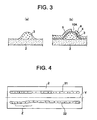
- the glaze layer 3 is usually formed with a semi-gabled transversal surface as illustrated in FIG. 3(a) by screen printing, for example. As shown in FIG. 3(b) , the heating-resistor layer 4 and the conductive layer are stacked thereon. The photo-engraving is applied to the conductive layer to form the common electrode 5 and separated electrodes 6 with a gap 10A between the tips thereof.
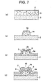
- several glaze layers for example, glaze layers 31 and 32 are simultaneously formed on a main surface of one ceramic substrate 2 followed by cutting on a dashed line Y to form a substrate (glazed ceramic substrate) having two glaze layers.
- the conventional thermal head since the conventional thermal head has a semi-gabled cross section, shifting of portions (recording section) at which electrodes facing each other if occur during patterning causes variation in height of the recording section from the substrate surface. Moreover, in formation of several glazed layers, wrinkles formed on a plate during screen printing could lower accuracy in straightness, thus causing undulation Z on a part of the glaze layer 2. Due to these problems, even photo-engraving, a highly accurate electrode forming step, is applied to the conductive layer, as illustrated in FIG. 5 , the recording section 10, which has to be located on the summit of the semi-gabled structure, is shifted from the summit, thus lowering printing quality.
- JP 08-207334 A a thermal head and its manufacture is known, according to which a partial glaze having a cross section of a projection is formed at an alumina substrate, wherein a heat-generating element consisting of a heat-generating resistance body film and electrodes is formed on the partial glaze.
- a thermal print head which has a substrate formed of heat insulating material, at least one glaze layer on a top surface of the substrate extending longitudinally thereof, a plurality of heat generating elements on the glaze layer, a plurality of electrodes each connected to the heat generating elements in a manner to form an opening for the heat generating elements and a protective layer for preventing the electrodes and heat generating elements from contacting the printing sheet to avoid their wear.
- a thermal head and its manufacture wherein a heat-generating laminate part of a thermal head comprises a protecting layer, a heat-generating resistance body, a common electrode and an individual electrode set on the heat-generating resistance body, and a barrier layer which is interposed between a heat-generating part constituted of the electrodes and the heat-generating resistance body and a heat accumulation layer.
- the object of the present invention is to improve a thermal head and a corresponding method for producing a thermal head.
- a thermal head and a method of producing the thermal head described herein provide the advantage of protecting a recording section from being shifted in height from a substrate, thereby attaining a higher printing quality and reliability and also a simplified production process.
- thermal head and a method of producing the thermal head described herein is that a recording section is protected from being shifted, which may otherwise occur due to shifting of a heating-resistor layer and separated electrodes caused by undulation of a glaze layer.
- a thermal head according to the first aspect of the present invention is defined in claim 1.
- a method of producing a thermal head according to the second aspect of the present invention is defined in claim 4
- the thermal head and the method of producing the thermal head according to each aspect provides the heat-retention layer of high straightness formed on the ceramic substrate with the sticking-out section of the glaze layer and also the recording section formed, between the tips of the common electrode and the separated electrodes, on the flat summit surface of the sticking-out section, thus achieving precise control of height of the recording section from the substrate for higher printing quality and reliability.
- FIG. 6 is a cross sectional view of the first embodiment of a thermal head according to the present invention. Elements in this drawing referenced by the reference numbers the same as in FIGS. 1 to 5 are identical to the counterparts shown in FIGS. 1 to 5 .
- the thermal head of the first embodiment shown in FIG. 6 is a type provided with a sticking-out glaze layer and a heating-resistor layer formed only on the flat summit of the sticking-out glaze layer.
- the thermal head of the first embodiment is formed with a glaze layer 3a lying in straight in the longitudinal direction on a main surface of the ceramic substrate 2.
- the glaze layer 3a has a semi-gabled shape having a summit of almost flat cross section and almost constant width.
- a heating-resistor member 4a made of a resistive material at a certain thickness.
- the glaze layer 3a and the heating-resistor member 4a make up a sticking-out section.
- the common electrode 5 and separated electrodes 6 which extend on both sides of the glaze layer 3a from a main surface of the ceramic substrate 2 to the side faces of the glaze layer 3a and further to the surface of the heating-resistor member 4a, the tips of the electrodes 5 and 6 facing each other with a predetermined gap.
- a protective layer 7 is formed in a predetermined region covering the common electrode 5 and separated electrodes 6.
- the protective layer 7 is formed to cover all elements, particularly, as shown in FIG. 6 , the tips of the common electrode 5 and separated electrodes 6 provided at both edges of the heating-resistor layer 4a formed on the summit of the sticking-out glaze layer 3a, and also the center portion of the summit corresponding to the gap.
- the center recording section 10 thus has a concave surface which is curved inwards in the middle a little bit.
- the glaze layer 3 is formed on the entire main surface of the ceramic substrate 2, followed by a thin film formation step, such as, sputtering, to form the heating-resistor layer 4 made of Ta-SiO on the glaze layer 3 used as the support base.
- the glaze layer is formed by applying glass paste on the substrate with a squeegee followed by drying and burning steps.
- a photoresist, etc. (not shown) is applied over the substrate 2 to have a straight portion of a predetermined width in the longitudinal direction through exposure and developing followed by etching using HF (hydrogen fluoride) as an etchant.
- HF hydrogen fluoride
- These steps provide a sticking-out section in which the heating-resistor member 4a is formed, by like self-alignment, on the summit (of almost constant width) of the glaze layer-sticking-out section 3a having a semi-gabled cross section.
- the heating-resistor member 4a has a shape similar to the summit of the glaze layer-sticking-out section 3a.
- An Al-film which will be formed as an electrode is formed on the substrate 2 by a thin-film forming method, such as, sputtering, followed by a photo-engraving process, thus forming, as illustrated in FIG. 7(c) , the common electrode 5 and separated electrodes 6 which extend from one main surface of the ceramic substrate 2 on both side faces of the glaze layer-sticking-out section 3a to the side faces of the section 3a and further to the surface of the heating-resistor member 4a.
- the comb-like tips of the common electrode 5 and separated electrodes 6 face each other with a predetermined gap.
- the accuracy of straightness in the photo-engraving process is ⁇ 10 ⁇ m to a 300 mm-long straight line. Thus, undulation is prevented from occurring on the glaze layer-sticking-out section 3a, which is the problem for the conventional thermal head.
- the protective layer 7 is formed using a sintered compact, a mixture of Si 3 -N 4 and SiO 2 , as a film forming base, to protect the tips of the common electrode 5 and separated electrodes 6 facing each other.
- Process requirements for etching is as follows: The first embodiment employs HF of 50% concentration as an etchant at an etching rate of about 1 ⁇ m/sec (1 ⁇ m-depth etching per second).
- HF + H 2 SO 4 sulfuric acid fluoride
- HF sulfuric acid fluoride
- the summit surface of the sticking-out section is substantially flat, maintaining flatness of the summit surface of the glaze layer before patterning.
- the surface roughness of the glaze layer after the sintering step is regarded as a substantially flat level.
- the structure and the production method disclosed above provides the thermal head having the sticking-out pattern with high straightness and the recording section 10 accurately formed on the flat summit of the sticking-out section, thus enhancing printing quality and reliability, and also providing a simplified production process only with thin-film forming step which has generally been used.
- FIG. 8 is a cross sectional view of the second embodiment of a thermal head according to the present invention. Elements in the second embodiment that are the same as or analogous to elements in the first embodiment shown in FIG. 6 are referenced by the same reference numerals and will not be explained in detail.
- the thermal head of the second embodiment shown in FIG .8 is a type provided with a glaze layer having a sticking-out section and a skirt section and a heating-resistor layer formed only on the flat summit of the sticking-out glaze layer.
- the second embodiment is, like the first embodiment, formed with the glaze layer 3a lying in straight in the longitudinal direction on a main surface of the ceramic substrate 2.
- the glaze layer 3a has a semi-gabled shape having a summit almost flat cross section and almost constant width.
- the glaze layer-sticking-out section 3a has a glaze layer-skirt section 3b on both sides thereof.
- the common electrode 5 and separated electrodes 6 are formed on the surface of the glaze layer skirt section 3b, the side face of the glaze layer-sticking-out section 3a and the surface of the heating-resistor member 4a.
- the glaze layer 3 is formed on the entire main surface of the ceramic substrate 2, followed by a thin film formation step, such as, sputtering, to form the heating-resistor layer 4 made of Ta-SiO on the glaze layer 3 used as the support base.
- a photoresist, etc. (not shown) is applied over the substrate 2 for exposure and developing followed by etching using 90%-HF, as an as illustrated in FIG. 9(b) , to have the glaze layer-sticking-out section 3a with a predetermined width in straight in the longitudinal direction of the ceramic substrate 2.
- the etching is halted to have the glaze layer-skirt section 3b with thickness about one-half of the glaze layer-sticking-out section 3a.
- the etching time is about one minute.
- An Al-film which will be formed as an electrode is formed on the substrate 2 by a thin-film forming method, such as, sputtering, followed by a photo-engraving process, thus forming, as illustrated in FIG. 9(c) , the common electrode 5 and separated electrodes 6 which extend from the glaze layer-skirt section 3b to the side faces of the glaze layer-sticking-out section 3a and further to the surface of the heating-resistor member 4a.
- the comb-like tips of the common electrode 5 and separated electrodes 6 face each other with a predetermined gap.
- the protective layer 7 is formed using a sintered compact, a mixture of Si 3 -N 4 and SiO 2 , as a film forming base, to protect the tips of the common electrode 5 and separated electrodes 6 facing each other.
- the structure and the production method disclosed above provides the thermal head having the heat-retention layer pattern with high straightness and the recording section 10 accurately formed on almost center of the summit of heat-retention layer in width direction, thus enhancing printing quality and reliability, and also providing a simplified production process.
- the second embodiment achieves leveling of the surface of the ceramic substrate 2 with the glaze layer-skirt section 3b, thus enhancing contact of separated electrodes 5 and the common electrode 6.
- the glaze layer-skirt section 3b further serves to release heat from the electrodes.
- the method of producing the thermal head in the first embodiment shown in FIG. 6 continues HF-etching until the both side faces of the glaze layer-sticking-out section 3a are etched out, which could lower contact of the section 3a to the ceramic substrate 2.
- contact to the ceramic substrate 2 is made by both the glaze layer-sticking-out section 3a and the glaze layer-skirt section 3b for firm contact.
- FIGS. 10 and FIGS. 11(a) to 11(e) Disclosed next with reference to FIGS. 10 and FIGS. 11(a) to 11(e) are a thermal head and a method of producing the thermal head which do not form part of the invention but are helpful for understanding the invention. Elements in this first background example that are the same as or analogous to elements in the first and the second embodiments are referenced by the same reference numerals.
- the thermal head shown in FIG. 10 is a type provided with a glaze layer having a sticking-out section and a skirt section and a heating-resistor layer formed over the sticking-out section and the skirt section of the glaze layer.
- the thermal head in the first background example is formed with a glaze layer having the skirt section 3b formed on a main surface of the ceramic substrate 2 at a almost constant thickness and a sticking-out section 3a as a heat-retention layer having an almost flat summit, lying in straight in the longitudinal detection of the substrate 2 and sticking out from the skirt section 3b.
- the heating-resistor member 4 is formed to cover the surface of the skirt section 3b, and both side faces of the summit of the sticking-out section 3a of the glaze layer 3.
- the common electrode 5 and separated electrodes 6 are formed on the skirt section 3b and the side faces of the sticking-out section 3a of the glaze layer 3, the tips of the common electrode 5 and separated electrodes 6 being electrically connected to the heating-resistor member 4 with a gap including the thickness of the member 4.
- the glaze layer 3 is formed on the entire main surface of the ceramic substrate 2, followed by applying a photoresist, etc., (not shown) over the substrate 2 for exposure and developing, and further by etching using 50%-HF, as illustrated in FIG. 11(b) , to have the glaze layer-sticking-out section 3a with a predetermined width in straight in the longitudinal direction of the ceramic substrate 2.
- the etching is halted to have the glaze layer-skirt section 3b with thickness about one-half of the glaze layer-sticking-out section 3a.
- the etching time is about one minute.
- the heating-resistor layer 4 made of Ta-SiO is formed by a thin-film forming method, such as, sputtering, using the glaze layer-sticking-out section 3a and the glaze layer-skirt section 3b as the support base.
- An Al-film which will be formed as an electrode is formed by a thin-film forming method, such as, sputtering, followed by a photo-engraving process, thus forming, as illustrated in FIG. 11(d) , the common electrode 5 and separated electrodes 6 on the surface of the heating-resistor member 4 on the side faces of the glaze layer-sticking-out section 3a and the surface of the glaze layer-skirt section 3b.
- the comb-like tips of the common electrode 5 and separated electrodes 6 face each other with a predetermined gap.
- the protective layer 7 is formed using a sintered.compact, a mixture of Si 3 -N 4 and SiO 2 , as a film forming base, to protect the tips of the common electrode 5 and separated electrodes 6 facing each other.
- the structure and the production method disclosed above provides the thermal head having the pattern with high straightness and the recording section 10 accurately formed on the summit of the sticking-out section in width direction, thus enhancing printing quality and reliability, and also providing a simplified production process.
- the glaze layer-skirt section 3b serves to enhance contact between separated electrodes 5 and the common electrode 6 and adjust the heat-retention characteristics with the heat-releasing function.
- the thermal head shown in FIG. 12 is a type provided with a glaze layer having a sticking-out section only and a heating-resistor layer formed over the substrate excluding the sticking-out section and the also over the sticking-out glaze layer.
- the second background example is formed with a glaze layer having the sticking-out section 3a only, as a heat-retention layer, having an almost flat summit.
- the heating-resistor member 4 is formed to cover the entire surface extending from a main surface of the substrate 2 to the side faces of the glaze layer-sticking-out section 3a and further to the flat summit.
- the common electrode 5 and separated electrodes 6 are formed on the surface of the heating-resistor member 4 excluding the surface the sticking-out section 3a and the side faces of the section 3a, the tips of the common electrode 5 and separated electrodes 6 being electrically connected to the heating-resistor member 4 with a gap including the width of the sticking-out section 3a and the thickness of the heating-resistor member 4 formed on the side faces of the sticking-out section 3a.
- FIG. 13(a) to 13(e) Disclosed next with reference to FIG. 13(a) to 13(e) is a method of producing the thermal head shown in FIG. 12 .
- the glaze layer 3 is formed on the entire main surface of the ceramic substrate 2, followed by applying a photoresist, etc., (not shown) over the substrate 2 for exposure and developing, and further by etching using 50%-HF, as illustrated in FIG. 13(b) , to have the glaze layer-sticking-out section 3a with a predetermined width in straight in the longitudinal direction of the ceramic substrate 2, The etching being halted in this state.
- the etching time is about one minute.
- the heating-resistor layer 4 made of Ta-SiO is formed by a thin-film forming method, such as, sputtering, using the glaze layer-sticking-out section 3a and the substrate 2 as the support base.
- An Al-film which will be formed as an electrode is formed by a thin-film forming method, such as, sputtering, followed by a photo-engraving process, thus forming, as illustrated in FIG. 13(d) , the common electrode 5 and separated electrodes 6 on the surface of the heating-resistor member 4 on the substrate 2 where no glaze layer has been formed from the entire glaze layer-sticking-out section 3a.
- the comb-like tips of the common electrode 5 and separated electrodes 6 face each other with a predetermined gap.
- the protective layer 7 is formed using a sintered compact, a mixture of Si 3 -N 4 and SiO 2 , as a film forming base, to protect the tips of the common electrode 5 and separated electrodes 6 facing each other. Production is then completed for the thermal head having the glaze layer of the sticking-out section 3a only.
- the structure and the production method disclosed above provides the thermal head having the pattern with high accuracy and the recording section 10 formed on the flat summit of the heat-retention layer, thus enhancing printing quality and reliability, and also providing a simplified production process.
- embodiments of the present invention achieve enhanced printing quality with protection of the recording section from being shifted in height from the substrate surface, and also achieve high reliability and simplicity in production process.
Landscapes
- Engineering & Computer Science (AREA)
- Manufacturing & Machinery (AREA)
- Electronic Switches (AREA)
Abstract
Description
- The present invention relates to a method of producing a thermal head. Particularly, this invention relates to the structure of a thermal head and a method of producing the thermal head, which offer high recording quality with improvement in the structure of a recording section for recording on a recording medium inserted between a platen and the recording section, for prevention of shifting of the recording section from a correct position to be recorded.
- Thermal heads have an important place in the fields of OA (Office Automation)-devices and fax machines. A thermal head is made up of heating resistors arranged on a substrate. The heating resistors generate heat for recording on heat-sensitive papers or films of type-setting developing paper. Several developments have been in progress for their low noise level and low running cost. Thermal heads have recently attracted attention as being used for video printers, for example.
-
FIG. 1 is a plan view of an overall structure of a conventional thermal head, partially cut away in several stages for easy understanding.FIG. 2 is an enlarged cross sectional view taken on arrows X - X of the thermal head shown inFIG. 1 . In these drawings, the thermal head is provided with analuminum substrate 1 formed with long narrow flat surface and having thickness for certain rigidity, aceramic substrate 2 formed on a main surface of thealuminum substrate 1 and having a thickness of 0.5 to 1. 0 mm, thermal resistance and relatively large coefficient of heat transfer, and several integrated circuits 8 (abbreviated to IC hereinafter) aligned in row at the side of theceramic substrate 2. Formed on the center portion of theceramic substrate 2 in the width direction in this structure is aglaze layer 3 as a heat-retention layer having a semi-gabled transversal surface formed in the longitudinal direction. A heating-resistor layer 4 is formed on the surface of theceramic substrate 2 including theglaze layer 3. - The
glaze layer 3 is mainly made of glass. The heating-resistor layer 4 includes an alloy, such as, Ta-SiO and made by a thin-film forming method, such as, sputtering. A conductive layer of aluminum, for example, is formed on the surface of the heating-resistor layer 4, and further, acommon electrode 5 and separatedelectrodes 6 are formed thereon by photo-engraving. Thecommon electrode 5 is formed like teeth of a comb on the one side of theglaze layer 3 from the center thereof.Several electrodes 6 are formed at theIC 8 side like strips aligned like teeth of a comb. The tips of thecommon electrode 5 and those of theseparated electrodes 6 face each other at the summit of thesemi-gabled glaze layer 3 with a predetermined gap. Connected to the other edge of each separatedelectrode 6 is alead wire 9 extended from theIC 8. A heat- and abrasion-resistant protective-film layer 7 is formed by, for example, sputtering, over the surfaces of thecommon electrode 5 and theelectrodes 6. - In this structure, a
recording section 10 covers the summit of the protective-film layer 7 formed over theglaze layer 3 and the surrounding, as a thermal head having resolution of 220 to 400 d/i (the number of dots per inch). - The thermal head described above is provided with the
recording section 10 at the portion corresponding to the summit of theglaze layer 3, thus having thecommon electrode 5 and theseparated electrodes 6 with the tips of comb-like teeth facing each other over the center summit. The positions of the tips facing each other are sometimes shifted from the correct positions due to incomplete production process. This problem is discussed with respect toFIGS. 3 to 5 . - The
glaze layer 3 is usually formed with a semi-gabled transversal surface as illustrated inFIG. 3(a) by screen printing, for example. As shown inFIG. 3(b) , the heating-resistor layer 4 and the conductive layer are stacked thereon. The photo-engraving is applied to the conductive layer to form thecommon electrode 5 and separatedelectrodes 6 with agap 10A between the tips thereof. In the process of forming theglaze layer 3 on theceramic substrate 2, as illustrated inFIG. 4 , several glaze layers, for example,glaze layers ceramic substrate 2 followed by cutting on a dashed line Y to form a substrate (glazed ceramic substrate) having two glaze layers. - As described, since the conventional thermal head has a semi-gabled cross section, shifting of portions (recording section) at which electrodes facing each other if occur during patterning causes variation in height of the recording section from the substrate surface. Moreover, in formation of several glazed layers, wrinkles formed on a plate during screen printing could lower accuracy in straightness, thus causing undulation Z on a part of the
glaze layer 2. Due to these problems, even photo-engraving, a highly accurate electrode forming step, is applied to the conductive layer, as illustrated inFIG. 5 , therecording section 10, which has to be located on the summit of the semi-gabled structure, is shifted from the summit, thus lowering printing quality. - From
JP 08-207334 A - Further, from
US 4,707,708 a thermal print head is known, which has a substrate formed of heat insulating material, at least one glaze layer on a top surface of the substrate extending longitudinally thereof, a plurality of heat generating elements on the glaze layer, a plurality of electrodes each connected to the heat generating elements in a manner to form an opening for the heat generating elements and a protective layer for preventing the electrodes and heat generating elements from contacting the printing sheet to avoid their wear. - Further, from
JP 11-034373 a - The object of the present invention is to improve a thermal head and a corresponding method for producing a thermal head.
- A thermal head and a method of producing the thermal head described herein provide the advantage of protecting a recording section from being shifted in height from a substrate, thereby attaining a higher printing quality and reliability and also a simplified production process.
- Another advantage of a thermal head and a method of producing the thermal head described herein is that a recording section is protected from being shifted, which may otherwise occur due to shifting of a heating-resistor layer and separated electrodes caused by undulation of a glaze layer.
- A thermal head according to the first aspect of the present invention is defined in
claim 1. - A method of producing a thermal head according to the second aspect of the present invention is defined in
claim 4 - The thermal head and the method of producing the thermal head according to each aspect provides the heat-retention layer of high straightness formed on the ceramic substrate with the sticking-out section of the glaze layer and also the recording section formed, between the tips of the common electrode and the separated electrodes, on the flat summit surface of the sticking-out section, thus achieving precise control of height of the recording section from the substrate for higher printing quality and reliability.
-
FIG. 1 shows a plan view of an overall structure of a conventional thermal head, partially cut away in several stages; -
FIG. 2 shows an enlarged cross sectional view of the conventional thermal head shown inFIG. 1 ; -
FIG. 3 shows cross sectional views (a) and (b) for explaining a production method of the conventional thermal head shown inFIG. 1 ; -
FIG. 4 is a plan view for explaining a production method of the conventional thermal head shown inFIG. 1 ; -
FIG. 5 is a cross sectional view of a structure of the conventional thermal head shown inFIG. 1 , exhibiting a poor printing performance; -
FIG. 6 is a cross sectional view of the first embodiment of a thermal head according to the present invention; -
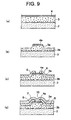
FIG. 7 shows cross sectional views (a) to (d) for explaining a production method of the first embodiment of the thermal head shown inFIG. 6 ; -
FIG. 8 is a cross sectional view of the second embodiment of a thermal head according to the present invention; -
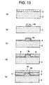
FIG. 9 shows cross sectional views (a) to (d) for explaining a production method of the second embodiment of the thermal head shown inFIG. 8 ; -
FIG. 10 is a cross sectional view of a first background example of a thermal head, which does not form part of the invention but is helpful for understanding the present invention; -
FIG. 11 shows cross sectional views (a) to (e) for explaining a production method of the thermal head shown inFIG. 10 ; -
FIG. 12 is a cross sectional view of a second background example of a thermal head, which does not form part of the invention but is helpful for understanding the present invention; and -
FIG. 13 shows cross sectional views (a) to (e) for explaining a production method of the thermal head shown inFIG. 12 . - Preferred embodiments according to the present invention will be disclosed with reference to the attached drawings.
-
FIG. 6 is a cross sectional view of the first embodiment of a thermal head according to the present invention. Elements in this drawing referenced by the reference numbers the same as inFIGS. 1 to 5 are identical to the counterparts shown inFIGS. 1 to 5 . The thermal head of the first embodiment shown inFIG. 6 is a type provided with a sticking-out glaze layer and a heating-resistor layer formed only on the flat summit of the sticking-out glaze layer. - The thermal head of the first embodiment is formed with a
glaze layer 3a lying in straight in the longitudinal direction on a main surface of theceramic substrate 2. Theglaze layer 3a has a semi-gabled shape having a summit of almost flat cross section and almost constant width. Formed on the summit of theglaze layer 3a is a heating-resistor member 4a made of a resistive material at a certain thickness. Theglaze layer 3a and the heating-resistor member 4a make up a sticking-out section. Also provided are thecommon electrode 5 and separatedelectrodes 6 which extend on both sides of theglaze layer 3a from a main surface of theceramic substrate 2 to the side faces of theglaze layer 3a and further to the surface of the heating-resistor member 4a, the tips of theelectrodes protective layer 7 is formed in a predetermined region covering thecommon electrode 5 and separatedelectrodes 6. Theprotective layer 7 is formed to cover all elements, particularly, as shown inFIG. 6 , the tips of thecommon electrode 5 and separatedelectrodes 6 provided at both edges of the heating-resistor layer 4a formed on the summit of the sticking-outglaze layer 3a, and also the center portion of the summit corresponding to the gap. Thecenter recording section 10 thus has a concave surface which is curved inwards in the middle a little bit. - Disclosed in detail, but focusing on the elements formed on the
ceramic substrate 2, with reference toFIGS. 7(a) to 7(d) , is a method of producing the thermal head in the first embodiment. - As illustrated in
FIG. 7(a) , theglaze layer 3 is formed on the entire main surface of theceramic substrate 2, followed by a thin film formation step, such as, sputtering, to form the heating-resistor layer 4 made of Ta-SiO on theglaze layer 3 used as the support base. The glaze layer is formed by applying glass paste on the substrate with a squeegee followed by drying and burning steps. - Next, as illustrated in
FIG. 7(b) , a photoresist, etc., (not shown) is applied over thesubstrate 2 to have a straight portion of a predetermined width in the longitudinal direction through exposure and developing followed by etching using HF (hydrogen fluoride) as an etchant. These steps provide a sticking-out section in which the heating-resistor member 4a is formed, by like self-alignment, on the summit (of almost constant width) of the glaze layer-sticking-outsection 3a having a semi-gabled cross section. The heating-resistor member 4a has a shape similar to the summit of the glaze layer-sticking-outsection 3a. - An Al-film which will be formed as an electrode is formed on the
substrate 2 by a thin-film forming method, such as, sputtering, followed by a photo-engraving process, thus forming, as illustrated inFIG. 7(c) , thecommon electrode 5 and separatedelectrodes 6 which extend from one main surface of theceramic substrate 2 on both side faces of the glaze layer-sticking-outsection 3a to the side faces of thesection 3a and further to the surface of the heating-resistor member 4a. The comb-like tips of thecommon electrode 5 and separatedelectrodes 6 face each other with a predetermined gap. The accuracy of straightness in the photo-engraving process is ± 10 µm to a 300 mm-long straight line. Thus, undulation is prevented from occurring on the glaze layer-sticking-outsection 3a, which is the problem for the conventional thermal head. - Next, as illustrated in
FIG. 7(d) , theprotective layer 7 is formed using a sintered compact, a mixture of Si3-N4 and SiO2, as a film forming base, to protect the tips of thecommon electrode 5 and separatedelectrodes 6 facing each other. Process requirements for etching is as follows: The first embodiment employs HF of 50% concentration as an etchant at an etching rate of about 1 µm/sec (1 µm-depth etching per second). As for the etchant and etching rate, it is preferable to employ HF + H2SO4 (sulfuric acid fluoride) of 50% concentration as an etchant at an etching rate of about 1 µm/sec, or HF of 50% concentration as an etchant at an etching rate of about 0. 2 µm/sec. - The summit surface of the sticking-out section is substantially flat, maintaining flatness of the summit surface of the glaze layer before patterning. In other words, the surface roughness of the glaze layer after the sintering step is regarded as a substantially flat level.
- The structure and the production method disclosed above provides the thermal head having the sticking-out pattern with high straightness and the
recording section 10 accurately formed on the flat summit of the sticking-out section, thus enhancing printing quality and reliability, and also providing a simplified production process only with thin-film forming step which has generally been used. -
FIG. 8 is a cross sectional view of the second embodiment of a thermal head according to the present invention. Elements in the second embodiment that are the same as or analogous to elements in the first embodiment shown inFIG. 6 are referenced by the same reference numerals and will not be explained in detail. The thermal head of the second embodiment shown inFIG .8 is a type provided with a glaze layer having a sticking-out section and a skirt section and a heating-resistor layer formed only on the flat summit of the sticking-out glaze layer. - The second embodiment is, like the first embodiment, formed with the
glaze layer 3a lying in straight in the longitudinal direction on a main surface of theceramic substrate 2. Theglaze layer 3a has a semi-gabled shape having a summit almost flat cross section and almost constant width. The glaze layer-sticking-outsection 3a, however, has a glaze layer-skirt section 3b on both sides thereof. Furthermore, thecommon electrode 5 and separatedelectrodes 6 are formed on the surface of the glazelayer skirt section 3b, the side face of the glaze layer-sticking-outsection 3a and the surface of the heating-resistor member 4a. These are the differences in structure with respect toFIG. 6 . Disclosed in detail, focusing on the elements formed on theceramic substrate 2, with reference toFIGS. 9(a) to 9(d) is a method of producing the thermal head in the second embodiment. - As illustrated in
FIG. 9(a) , theglaze layer 3 is formed on the entire main surface of theceramic substrate 2, followed by a thin film formation step, such as, sputtering, to form the heating-resistor layer 4 made of Ta-SiO on theglaze layer 3 used as the support base. Next, a photoresist, etc., (not shown) is applied over thesubstrate 2 for exposure and developing followed by etching using 90%-HF, as an as illustrated inFIG. 9(b) , to have the glaze layer-sticking-outsection 3a with a predetermined width in straight in the longitudinal direction of theceramic substrate 2. The etching is halted to have the glaze layer-skirt section 3b with thickness about one-half of the glaze layer-sticking-outsection 3a. The etching time is about one minute. - An Al-film which will be formed as an electrode is formed on the
substrate 2 by a thin-film forming method, such as, sputtering, followed by a photo-engraving process, thus forming, as illustrated inFIG. 9(c) , thecommon electrode 5 and separatedelectrodes 6 which extend from the glaze layer-skirt section 3b to the side faces of the glaze layer-sticking-outsection 3a and further to the surface of the heating-resistor member 4a. The comb-like tips of thecommon electrode 5 and separatedelectrodes 6 face each other with a predetermined gap. - Next, as illustrated in
FIG. 9(d) , theprotective layer 7 is formed using a sintered compact, a mixture of Si3-N4 and SiO2, as a film forming base, to protect the tips of thecommon electrode 5 and separatedelectrodes 6 facing each other. - The structure and the production method disclosed above provides the thermal head having the heat-retention layer pattern with high straightness and the
recording section 10 accurately formed on almost center of the summit of heat-retention layer in width direction, thus enhancing printing quality and reliability, and also providing a simplified production process. Moreover, the second embodiment achieves leveling of the surface of theceramic substrate 2 with the glaze layer-skirt section 3b, thus enhancing contact of separatedelectrodes 5 and thecommon electrode 6. The glaze layer-skirt section 3b further serves to release heat from the electrodes. - The method of producing the thermal head in the first embodiment shown in
FIG. 6 continues HF-etching until the both side faces of the glaze layer-sticking-outsection 3a are etched out, which could lower contact of thesection 3a to theceramic substrate 2. In the second embodiment, however, contact to theceramic substrate 2 is made by both the glaze layer-sticking-outsection 3a and the glaze layer-skirt section 3b for firm contact. - Disclosed next with reference to
FIGS. 10 andFIGS. 11(a) to 11(e) are a thermal head and a method of producing the thermal head which do not form part of the invention but are helpful for understanding the invention. Elements in this first background example that are the same as or analogous to elements in the first and the second embodiments are referenced by the same reference numerals. The thermal head shown inFIG. 10 is a type provided with a glaze layer having a sticking-out section and a skirt section and a heating-resistor layer formed over the sticking-out section and the skirt section of the glaze layer. - The thermal head in the first background example is formed with a glaze layer having the
skirt section 3b formed on a main surface of theceramic substrate 2 at a almost constant thickness and a sticking-outsection 3a as a heat-retention layer having an almost flat summit, lying in straight in the longitudinal detection of thesubstrate 2 and sticking out from theskirt section 3b. The heating-resistor member 4 is formed to cover the surface of theskirt section 3b, and both side faces of the summit of the sticking-outsection 3a of theglaze layer 3. Thecommon electrode 5 and separatedelectrodes 6 are formed on theskirt section 3b and the side faces of the sticking-outsection 3a of theglaze layer 3, the tips of thecommon electrode 5 and separatedelectrodes 6 being electrically connected to the heating-resistor member 4 with a gap including the thickness of themember 4. - In this structure, the summits of separated electrodes and the common electrode and the summit of the heating-resistor layer on the sticking-out section form an almost continuous plane. Disclosed next with reference to
FIG. 11(a) to 11(e) is a method of producing the thermal head shown inFIG. 10 . - As illustrated in
FIG. 11(a) , theglaze layer 3 is formed on the entire main surface of theceramic substrate 2, followed by applying a photoresist, etc., (not shown) over thesubstrate 2 for exposure and developing, and further by etching using 50%-HF, as illustrated inFIG. 11(b) , to have the glaze layer-sticking-outsection 3a with a predetermined width in straight in the longitudinal direction of theceramic substrate 2. The etching is halted to have the glaze layer-skirt section 3b with thickness about one-half of the glaze layer-sticking-outsection 3a. The etching time is about one minute. - Next, as illustrated in
FIG. 11(c) , the heating-resistor layer 4 made of Ta-SiO is formed by a thin-film forming method, such as, sputtering, using the glaze layer-sticking-outsection 3a and the glaze layer-skirt section 3b as the support base. - An Al-film which will be formed as an electrode is formed by a thin-film forming method, such as, sputtering, followed by a photo-engraving process, thus forming, as illustrated in
FIG. 11(d) , thecommon electrode 5 and separatedelectrodes 6 on the surface of the heating-resistor member 4 on the side faces of the glaze layer-sticking-outsection 3a and the surface of the glaze layer-skirt section 3b. The comb-like tips of thecommon electrode 5 and separatedelectrodes 6 face each other with a predetermined gap. - Next, as illustrated in
FIG. 11(e) , theprotective layer 7 is formed using a sintered.compact, a mixture of Si3-N4 and SiO2, as a film forming base, to protect the tips of thecommon electrode 5 and separatedelectrodes 6 facing each other. - The structure and the production method disclosed above provides the thermal head having the pattern with high straightness and the
recording section 10 accurately formed on the summit of the sticking-out section in width direction, thus enhancing printing quality and reliability, and also providing a simplified production process. - In the first background example, like the second embodiment, the glaze layer-
skirt section 3b serves to enhance contact betweenseparated electrodes 5 and thecommon electrode 6 and adjust the heat-retention characteristics with the heat-releasing function. - Disclosed next with reference to
FIGS. 12 andFIGS. 13(a) to 13(e) are a thermal head and a method of producing the thermal head in the second background example, which is helpful for understanding the invention. Elements in this example that are the same as or analogous to elements in the foregoing embodiments are referenced by the same reference numerals. The thermal head shown inFIG. 12 is a type provided with a glaze layer having a sticking-out section only and a heating-resistor layer formed over the substrate excluding the sticking-out section and the also over the sticking-out glaze layer. - In
FIG. 12 , the second background example is formed with a glaze layer having the sticking-outsection 3a only, as a heat-retention layer, having an almost flat summit. The heating-resistor member 4 is formed to cover the entire surface extending from a main surface of thesubstrate 2 to the side faces of the glaze layer-sticking-outsection 3a and further to the flat summit. Thecommon electrode 5 and separatedelectrodes 6 are formed on the surface of the heating-resistor member 4 excluding the surface the sticking-outsection 3a and the side faces of thesection 3a, the tips of thecommon electrode 5 and separatedelectrodes 6 being electrically connected to the heating-resistor member 4 with a gap including the width of the sticking-outsection 3a and the thickness of the heating-resistor member 4 formed on the side faces of the sticking-outsection 3a. - Disclosed next with reference to
FIG. 13(a) to 13(e) is a method of producing the thermal head shown inFIG. 12 . - As illustrated in
FIG. 13(a) , theglaze layer 3 is formed on the entire main surface of theceramic substrate 2, followed by applying a photoresist, etc., (not shown) over thesubstrate 2 for exposure and developing, and further by etching using 50%-HF, as illustrated inFIG. 13(b) , to have the glaze layer-sticking-outsection 3a with a predetermined width in straight in the longitudinal direction of theceramic substrate 2, The etching being halted in this state. The etching time is about one minute. - Next, as illustrated in
FIG. 13(c) , the heating-resistor layer 4 made of Ta-SiO is formed by a thin-film forming method, such as, sputtering, using the glaze layer-sticking-outsection 3a and thesubstrate 2 as the support base. - An Al-film which will be formed as an electrode is formed by a thin-film forming method, such as, sputtering, followed by a photo-engraving process, thus forming, as illustrated in
FIG. 13(d) , thecommon electrode 5 and separatedelectrodes 6 on the surface of the heating-resistor member 4 on thesubstrate 2 where no glaze layer has been formed from the entire glaze layer-sticking-outsection 3a. The comb-like tips of thecommon electrode 5 and separatedelectrodes 6 face each other with a predetermined gap. - Next, as illustrated in
FIG. 13(e) , theprotective layer 7 is formed using a sintered compact, a mixture of Si3-N4 and SiO2, as a film forming base, to protect the tips of thecommon electrode 5 and separatedelectrodes 6 facing each other. Production is then completed for the thermal head having the glaze layer of the sticking-outsection 3a only. - The structure and the production method disclosed above provides the thermal head having the pattern with high accuracy and the
recording section 10 formed on the flat summit of the heat-retention layer, thus enhancing printing quality and reliability, and also providing a simplified production process. - As disclosed above, embodiments of the present invention achieve enhanced printing quality with protection of the recording section from being shifted in height from the substrate surface, and also achieve high reliability and simplicity in production process.
Claims (6)
- A thermal head comprising:a longitudinal substrate (2);a heat-retention layer made of a heat-retaining material, having at least a sticking-out section (3a) lying on one main surface of the substrate (2) wherein said sticking-out section (3a) is longitudinally straight and arranged in the longitudinal direction of the substrate, said sticking-out section (3a) projects from the substrate or the heat-retention layer and has an almost flat summit surface with a constant width;a heating-resistor member (4a) made of a resistive material, formed on the almost flat summit surface of the sticking-out section (3a) of the heat-retention layer at a predetermined thickness and having a predetermined width same as said constant width of said almost flat summit surface of the sticking-out section (3a);a common electrode (5) located on and provided as touching the heating-resistor member (4a);a plurality of separated electrodes (6) located on said heating-resistor member (4a) and provided as facing a tip of the common electrode (5) with a gap, at least an edge of each separated electrode (6) touching the heating-resistor member (4a), another edge of each separated electrode (6) being connected to a driver circuit; anda protective layer (7) formed on the heating-resistor member (4a), a heating-resistor member portion provided in the gap between the common electrode (5) and the separated electrodes (6) functioning as a recording section, the recording section being formed on the flat summit surface, being at the centre of the
- The thermal head according to claim 1, wherein the common electrode (5) and the separated electrodes (6) are formed as rising from a side edge of the substrate (2) in the longitudinal direction to a side face of the sticking-out section (3a) of the heat-retention layer and covering a side edge, in the longitudinal direction, of the heating-resistor member (4a) formed on the summit surface.
- The thermal head, according to claim 1, wherein the heat-retention layer includes a skirt section (3b) formed on the main surface of the substrate (2) at an almost constant thickness, the sticking-out section (3a) being formed on the skirt section (3b) as sticking out therefrom.
- A method of producing a thermal head comprising the steps of:a step of applying a heat-retaining material on a main surface of a substrate (2), thus forming a heat-retention layer;a step of applying a resistive material on a surface of the heat-retention layer, thus forming a heating-resistor layer (4a);a step of forming a longitudinally straight sticking-out section (3a) arranged in a longitudinal direction of the substrate and projection from the substrate or the heat-retention layer by etching the heating-resistor layer (4a) and the heat-retention layer, said sticking-out section (3a) comprising an almost flat summit surface having a constant width same as a predetermined width of the heating-resistor layer (4a);a step of forming a common electrode (5), an edge thereof touching the heating-resistor layer (4a), and a plurality of separated electrodes (6) provided as facing tips of the common electrode (5) with a gap, at least one edge of each separated electrode touching the heating-resistor layer (4a), both of the edges of said common electrode (5) and separated electrodes (6) being located on said almost flat surface of the heating-resistor layer (4a);a step of defining a recording portion (10) as said gap being at the centre of the width direction of said flat summit surface of the heating-resistor layer (4a) ; anda step of forming a protective layer (7) at least on the heating-resistor layer (4a).
- The method of producing a thermal head according to claim 4, wherein the sticking-out section (3a) forming step includes the step of forming the sticking-out section (3a) lying in straight, having a flat summit, including the heating-resistor member (4a) on the flat surface of the heat-retention layer by etching the heat-retention layer and the heating-resistor member (4a) stacked on the main surface of the substrate (2), and the electrode forming step includes the step of forming the common electrode (5) and the separated electrodes (6) aligned like a row of teeth of a comb, the common electrode (5) and the separated electrodes (6) being provided from both sides of the sticking-out section (3a) to one main surface of the substrate (2), side faces of the heat-retention layer and a surface of the heating-resistor member (4a), the teeth facing each other with a predetermined gap being connected to the heating-resistor member (4a).
- The method of producing a thermal head according to claim 4, wherein the sticking-out section (3a) forming step includes the step of forming the sticking-out section (3a) lying in straight, having a flat summit, over the main surface of the substrate (2), including the heating-resistor member (4a) on the almost flat surface of the heat-retention layer, the sticking-out section (3a) having a skirt section (3b) on both sides thereof in its cross sectional shape by etching the heat-retention layer and the heating-resistor member (4a), and the electrode forming step includes the step of forming the common electrode (5) and the separated electrodes (6) aligned like a row of teeth of a comb, the common electrode (5) and the separated electrodes (6) being provided from both sides of the sticking-out section (3a) to the skirt section (3b) of the sticking-out section (3a), side faces thereof, and a surface of the heating-resistor member (4a), the teeth facing each other with a predetermined gap being connected to the heating-resistor member (4a).
Applications Claiming Priority (3)
| Application Number | Priority Date | Filing Date | Title |
|---|---|---|---|
| JP26928299 | 1999-09-22 | ||
| JP26928299 | 1999-09-22 | ||
| PCT/JP2000/006525 WO2001021409A1 (en) | 1999-09-22 | 2000-09-22 | Thermal head and method for manufacturing the same |
Publications (3)
| Publication Number | Publication Date |
|---|---|
| EP1243427A1 EP1243427A1 (en) | 2002-09-25 |
| EP1243427A4 EP1243427A4 (en) | 2002-11-06 |
| EP1243427B1 true EP1243427B1 (en) | 2012-03-07 |
Family
ID=17470195
Family Applications (1)
| Application Number | Title | Priority Date | Filing Date |
|---|---|---|---|
| EP00961206A Expired - Lifetime EP1243427B1 (en) | 1999-09-22 | 2000-09-22 | Thermal head and method for manufacturing the same |
Country Status (3)
| Country | Link |
|---|---|
| US (1) | US6753893B1 (en) |
| EP (1) | EP1243427B1 (en) |
| WO (1) | WO2001021409A1 (en) |
Families Citing this family (4)
| Publication number | Priority date | Publication date | Assignee | Title |
|---|---|---|---|---|
| US8154575B2 (en) * | 2007-10-23 | 2012-04-10 | Seiko Instruments Inc. | Heating resistor element, manufacturing method for the same, thermal head, and printer |
| JP2009184272A (en) * | 2008-02-07 | 2009-08-20 | Sony Corp | Thermal head, thermal printer, and thermal head manufacturing method |
| JP2017114051A (en) * | 2015-12-25 | 2017-06-29 | ローム株式会社 | Thermal print head |
| EP3260928B1 (en) * | 2016-06-20 | 2020-10-14 | Toshiba TEC Kabushiki Kaisha | Heater and heating device |
Family Cites Families (8)
| Publication number | Priority date | Publication date | Assignee | Title |
|---|---|---|---|---|
| JPS61107542U (en) * | 1984-12-19 | 1986-07-08 | ||
| US4707708A (en) | 1985-09-27 | 1987-11-17 | Hitachi, Ltd. | Thermal print head |
| JPH037354A (en) | 1988-07-01 | 1991-01-14 | Fuji Xerox Co Ltd | Thermal head and manufacture thereof |
| JPH08207334A (en) | 1995-02-06 | 1996-08-13 | Fuji Photo Film Co Ltd | Thermal head and its manufacture |
| US6151054A (en) * | 1997-03-28 | 2000-11-21 | Fuji Photo Film Co., Ltd. | Thermal head and method of manufacturing the same, and heat-sensitive recording method |
| JPH1134376A (en) * | 1997-07-23 | 1999-02-09 | Tdk Corp | Thermal head and fabrication thereof |
| JP3844155B2 (en) * | 1997-07-23 | 2006-11-08 | Tdk株式会社 | Manufacturing method of thermal head |
| JP3868755B2 (en) * | 2001-04-05 | 2007-01-17 | アルプス電気株式会社 | Thermal head and manufacturing method thereof |
-
2000
- 2000-09-22 EP EP00961206A patent/EP1243427B1/en not_active Expired - Lifetime
- 2000-09-22 WO PCT/JP2000/006525 patent/WO2001021409A1/en not_active Ceased
- 2000-09-22 US US10/088,087 patent/US6753893B1/en not_active Expired - Lifetime
Also Published As
| Publication number | Publication date |
|---|---|
| WO2001021409A1 (en) | 2001-03-29 |
| EP1243427A4 (en) | 2002-11-06 |
| US6753893B1 (en) | 2004-06-22 |
| EP1243427A1 (en) | 2002-09-25 |
Similar Documents
| Publication | Publication Date | Title |
|---|---|---|
| CN1636748A (en) | Thermal head, manufacturing method thereof, and method for adjusting dot aspect ratio of thermal head | |
| US5594488A (en) | Thermal head | |
| EP0763431B1 (en) | Thermal printing head, substrate used therefor and method for producing the substrate | |
| EP0829369B1 (en) | Thermal head and method of manufacturing the same | |
| US6753893B1 (en) | Thermal head and method for manufacturing the same | |
| JP4227799B2 (en) | Thermal head and manufacturing method thereof | |
| JP2001232838A (en) | Thermal printing head and manufacturing method | |
| JP3472755B2 (en) | Thermal head and method of manufacturing the same | |
| JP2801752B2 (en) | Thermal head | |
| JP2586008B2 (en) | Manufacturing method of thermal head | |
| JP3231951B2 (en) | Thermal head and method of manufacturing the same | |
| JPH0661947B2 (en) | Thermal head | |
| US4691210A (en) | Thermal head for heat-sensitive recording | |
| JP3470824B2 (en) | Thermal print head | |
| JP2579389B2 (en) | Thermal head | |
| JP2002002005A (en) | Thick film type thermal printing head | |
| US6330014B1 (en) | Thermal head manufactured by sequentially laminating conductive layer, layer insulating layer and heater element on heat insulating layer | |
| JPH03239562A (en) | Thermal head | |
| JPH0419155A (en) | Thick film type thermal head | |
| CN113386469B (en) | Thermal print head and method of manufacturing the same | |
| JP2004017523A (en) | Thermal head and its manufacturing process | |
| JP2527007Y2 (en) | Thermal head | |
| JP2561133B2 (en) | Electrode structure of thermal head | |
| JP2000246934A (en) | Thermal head | |
| JP2554556B2 (en) | Thermal print head |
Legal Events
| Date | Code | Title | Description |
|---|---|---|---|
| PUAI | Public reference made under article 153(3) epc to a published international application that has entered the european phase |
Free format text: ORIGINAL CODE: 0009012 |
|
| 17P | Request for examination filed |
Effective date: 20020416 |
|
| AK | Designated contracting states |
Kind code of ref document: A1 Designated state(s): AT BE CH CY DE DK ES FI FR GB GR IE IT LI LU MC NL PT SE |
|
| A4 | Supplementary search report drawn up and despatched | ||
| AK | Designated contracting states |
Kind code of ref document: A4 Designated state(s): AT BE CH CY DE DK ES FI FR GB GR IE IT LI LU MC NL PT SE |
|
| A4 | Supplementary search report drawn up and despatched |
Effective date: 20021106 |
|
| RBV | Designated contracting states (corrected) |
Designated state(s): AT BE CH DE FR GB LI |
|
| 17Q | First examination report despatched |
Effective date: 20041207 |
|
| 17Q | First examination report despatched |
Effective date: 20041207 |
|
| GRAP | Despatch of communication of intention to grant a patent |
Free format text: ORIGINAL CODE: EPIDOSNIGR1 |
|
| RBV | Designated contracting states (corrected) |
Designated state(s): DE FR GB |
|
| GRAS | Grant fee paid |
Free format text: ORIGINAL CODE: EPIDOSNIGR3 |
|
| GRAA | (expected) grant |
Free format text: ORIGINAL CODE: 0009210 |
|
| AK | Designated contracting states |
Kind code of ref document: B1 Designated state(s): DE FR GB |
|
| REG | Reference to a national code |
Ref country code: GB Ref legal event code: FG4D |
|
| REG | Reference to a national code |
Ref country code: DE Ref legal event code: R096 Ref document number: 60046983 Country of ref document: DE Effective date: 20120503 |
|
| PLBE | No opposition filed within time limit |
Free format text: ORIGINAL CODE: 0009261 |
|
| STAA | Information on the status of an ep patent application or granted ep patent |
Free format text: STATUS: NO OPPOSITION FILED WITHIN TIME LIMIT |
|
| 26N | No opposition filed |
Effective date: 20121210 |
|
| REG | Reference to a national code |
Ref country code: DE Ref legal event code: R097 Ref document number: 60046983 Country of ref document: DE Effective date: 20121210 |
|
| REG | Reference to a national code |
Ref country code: FR Ref legal event code: PLFP Year of fee payment: 16 |
|
| PGFP | Annual fee paid to national office [announced via postgrant information from national office to epo] |
Ref country code: DE Payment date: 20150916 Year of fee payment: 16 Ref country code: GB Payment date: 20150916 Year of fee payment: 16 |
|
| PGFP | Annual fee paid to national office [announced via postgrant information from national office to epo] |
Ref country code: FR Payment date: 20150811 Year of fee payment: 16 |
|
| REG | Reference to a national code |
Ref country code: DE Ref legal event code: R119 Ref document number: 60046983 Country of ref document: DE |
|
| GBPC | Gb: european patent ceased through non-payment of renewal fee |
Effective date: 20160922 |
|
| REG | Reference to a national code |
Ref country code: FR Ref legal event code: ST Effective date: 20170531 |
|
| PG25 | Lapsed in a contracting state [announced via postgrant information from national office to epo] |
Ref country code: DE Free format text: LAPSE BECAUSE OF NON-PAYMENT OF DUE FEES Effective date: 20170401 Ref country code: GB Free format text: LAPSE BECAUSE OF NON-PAYMENT OF DUE FEES Effective date: 20160922 Ref country code: FR Free format text: LAPSE BECAUSE OF NON-PAYMENT OF DUE FEES Effective date: 20160930 |