EP1241784A1 - Modulateur numerique - Google Patents
Modulateur numerique Download PDFInfo
- Publication number
- EP1241784A1 EP1241784A1 EP02075834A EP02075834A EP1241784A1 EP 1241784 A1 EP1241784 A1 EP 1241784A1 EP 02075834 A EP02075834 A EP 02075834A EP 02075834 A EP02075834 A EP 02075834A EP 1241784 A1 EP1241784 A1 EP 1241784A1
- Authority
- EP
- European Patent Office
- Prior art keywords
- signal
- interpolation
- digital
- sign
- signals
- Prior art date
- Legal status (The legal status is an assumption and is not a legal conclusion. Google has not performed a legal analysis and makes no representation as to the accuracy of the status listed.)
- Withdrawn
Links
- 238000001914 filtration Methods 0.000 claims description 12
- 238000000034 method Methods 0.000 claims description 5
- 238000003672 processing method Methods 0.000 claims description 5
- 239000000523 sample Substances 0.000 description 20
- 230000006870 function Effects 0.000 description 14
- 230000005540 biological transmission Effects 0.000 description 12
- 239000008186 active pharmaceutical agent Substances 0.000 description 8
- 101100012910 Plasmodium falciparum (isolate FC27 / Papua New Guinea) FIRA gene Proteins 0.000 description 7
- 238000004364 calculation method Methods 0.000 description 4
- 102100031456 Centriolin Human genes 0.000 description 3
- 101000941711 Homo sapiens Centriolin Proteins 0.000 description 3
- 238000001514 detection method Methods 0.000 description 3
- 238000010586 diagram Methods 0.000 description 3
- 238000002372 labelling Methods 0.000 description 3
- 230000000295 complement effect Effects 0.000 description 2
- 230000004069 differentiation Effects 0.000 description 2
- 239000013074 reference sample Substances 0.000 description 2
- 230000001934 delay Effects 0.000 description 1
- 230000003111 delayed effect Effects 0.000 description 1
- 230000000694 effects Effects 0.000 description 1
- 239000000835 fiber Substances 0.000 description 1
- 238000012886 linear function Methods 0.000 description 1
- 230000015654 memory Effects 0.000 description 1
- 230000003287 optical effect Effects 0.000 description 1
- 239000013307 optical fiber Substances 0.000 description 1
- 230000010363 phase shift Effects 0.000 description 1
- 230000000630 rising effect Effects 0.000 description 1
- 230000008054 signal transmission Effects 0.000 description 1
Images


Classifications
-
- H—ELECTRICITY
- H04—ELECTRIC COMMUNICATION TECHNIQUE
- H04L—TRANSMISSION OF DIGITAL INFORMATION, e.g. TELEGRAPHIC COMMUNICATION
- H04L7/00—Arrangements for synchronising receiver with transmitter
- H04L7/04—Speed or phase control by synchronisation signals
-
- H—ELECTRICITY
- H03—ELECTRONIC CIRCUITRY
- H03H—IMPEDANCE NETWORKS, e.g. RESONANT CIRCUITS; RESONATORS
- H03H17/00—Networks using digital techniques
- H03H17/02—Frequency selective networks
- H03H17/06—Non-recursive filters
- H03H17/0621—Non-recursive filters with input-sampling frequency and output-delivery frequency which differ, e.g. extrapolation; Anti-aliasing
- H03H17/0635—Non-recursive filters with input-sampling frequency and output-delivery frequency which differ, e.g. extrapolation; Anti-aliasing characterized by the ratio between the input-sampling and output-delivery frequencies
- H03H17/0642—Non-recursive filters with input-sampling frequency and output-delivery frequency which differ, e.g. extrapolation; Anti-aliasing characterized by the ratio between the input-sampling and output-delivery frequencies the ratio being arbitrary or irrational
-
- H—ELECTRICITY
- H03—ELECTRONIC CIRCUITRY
- H03H—IMPEDANCE NETWORKS, e.g. RESONANT CIRCUITS; RESONATORS
- H03H17/00—Networks using digital techniques
- H03H17/02—Frequency selective networks
- H03H17/06—Non-recursive filters
- H03H17/0621—Non-recursive filters with input-sampling frequency and output-delivery frequency which differ, e.g. extrapolation; Anti-aliasing
- H03H17/0628—Non-recursive filters with input-sampling frequency and output-delivery frequency which differ, e.g. extrapolation; Anti-aliasing the input and output signals being derived from two separate clocks, i.e. asynchronous sample rate conversion
-
- H—ELECTRICITY
- H03—ELECTRONIC CIRCUITRY
- H03H—IMPEDANCE NETWORKS, e.g. RESONANT CIRCUITS; RESONATORS
- H03H2218/00—Indexing scheme relating to details of digital filters
- H03H2218/08—Resource sharing
-
- H—ELECTRICITY
- H04—ELECTRIC COMMUNICATION TECHNIQUE
- H04L—TRANSMISSION OF DIGITAL INFORMATION, e.g. TELEGRAPHIC COMMUNICATION
- H04L7/00—Arrangements for synchronising receiver with transmitter
- H04L7/0016—Arrangements for synchronising receiver with transmitter correction of synchronization errors
- H04L7/002—Arrangements for synchronising receiver with transmitter correction of synchronization errors correction by interpolation
- H04L7/0029—Arrangements for synchronising receiver with transmitter correction of synchronization errors correction by interpolation interpolation of received data signal
-
- H—ELECTRICITY
- H04—ELECTRIC COMMUNICATION TECHNIQUE
- H04L—TRANSMISSION OF DIGITAL INFORMATION, e.g. TELEGRAPHIC COMMUNICATION
- H04L7/00—Arrangements for synchronising receiver with transmitter
- H04L7/0091—Transmitter details
Definitions
- the present invention relates to a digital modulator comprising a clock frequency and being capable of processing a digital signal comprising symbols sampled at a symbol frequency. It also relates to a signal processing method adapted to said modulator. It finds a particular application in particular during transmissions of digital signals via wired supports such as cable, aerials such as radio-relay systems or even optical supports such as optical fibers.
- the system includes a digital modulator.
- the modulator includes an oscillator which generates a fixed clock frequency.
- said signal is processed in the form of symbols to be transmitted.
- a symbol frequency is associated with the transmission of these symbols.
- this symbol frequency includes values fixed in standards such as DAVIC (Digital Audio-Visual Council), - DVB (Digital Video Broadcasting) published by ETSI (European Telecommunications Standard Institute ) referenced ETS300800 or DOCSIS (Data Over Cable Service Interface Specifications) published by the RFI (Radio Frequency Interface) referenced SP-RFI-104-98724.
- Said values are respectively 256 kbits / s or multiples of 1.544 Mbits / s or even 160 ksymb / s.
- the clock frequency of the modulator is appropriately associated.
- the clock frequency is chosen in such a way that it corresponds to the smallest common multiple of the symbol frequencies that can be used.
- the ratio between the clock frequency and the symbol frequency must be an integer and sometimes even a power of 2.
- a technical problem to be solved by the object of the present invention is to propose a digital modulator comprising a clock frequency and being capable of process a digital signal comprising symbols sampled at a frequency symbol, as well as an associated digital signal processing method, which would allow to simplify the management of symbol frequencies and to extend the range of frequencies symbols usable by said modulator.
- the interpolation means allow to process the digital signal in such a way that the clock frequency no longer depends of the symbol frequency (s) you wish to use.
- the choice of the ratio is free of all constraint. As a result, the management of symbol frequencies is more flexible and simplified.
- the present description of the invention relates to an example of a digital DM modulator used in the field of cable interactivity.
- signals digital signals are exchanged via a physical hybrid transmission channel such as a cable coaxial and fiber optic.
- the digital DM modulator allows the transmission of these signals through such a channel.
- Figure 1 is shown a diagram of an architecture of said DM modulator.
- Said modulator comprises a clock frequency Fclk, means for ENC error detection, RAND scrambling means, MAP labeling means, first FIR filtering means, INT interpolation means and means for MOD modulation on a carrier frequency Fca.
- the digital modulator DM receives as input a digital signal DS from a or several sources such as memories of a cable modem.
- Said DS signal is composed of bytes and is transmitted at a first frequency Fby in bytes / s.
- the modulator emits a sinusoidal signal.
- the digital signal DS is modulated on a carrier frequency Fca.
- the carrier frequency is determined by the standard used. So for the DVB standard, the carrier frequency can take a value between 5 MHz and 65 MHz, while for the DOCSIS standard, it takes a value between 5 MHz and 42 MHz.
- QPSK modulation in phase quadrature called in the English language “Quadrature Phase Shift Keying"
- the steps are described below.
- the means error detection ENC transforms said DS signal so that the errors will be detected and corrected thereafter.
- These ENC means are based on a principle of redundancy and likelihood called “Reed-Solomon", known to man of career.
- the digital signal is serialized in binary form according to a binary frequency Fbi in bits / s (one byte being equal to 8 bits).
- the SRC source emits a priori any bit sequences. Avoid the transmission of a constant sequence which would have the effect of transmitting on the CHA channel a high power pure frequency, which could damage the channel. .
- the RAND scrambling means scramble the digital signal with a pseudo-random sequence in order to make it pseudo-random, i.e. short term random
- the binary digital signal is not transmitted directly on the channel CHA. It is issued in the form of SYMB symbols.
- MAP labeling means recover by inputs the bits of the binary digital signal and encodes them as SYMB symbols
- each symbol SYMB codes two bits I and Q, which corresponds for example to the following coding.
- I Q SYMB 0 0 -1 -1 0 1 -1 1 1 1 1 1 1 1 0 1 -1
- the signal transmission is then represented by a symbol frequency Fsy.
- the binary frequency Fbi is equal to twice the symbol frequency Fsy.
- the CHA transmission channel has a bandwidth which is shared between different users. Therefore, the signal transmitted by each user is band limited. To do this, it is preferable to use first FIR filtering means. adapted. In addition, we seek with this filter to minimize inter-symbol interference (ISI) which cause a distortion of the transmitted signal.
- the INT interpolation means allow the signal to be oversampled.
- Fmax Fca + Fsy (1 + ⁇ ).
- ⁇ is the factor of fallout and is called "roll-off" in the English language and is equal to 30% in the standard DVB and 25% in the MCNS standard.
- the INT interpolation means are described in patent US05349548 issued in the name of the company PHILIPS ELECTRONICS NV and filed on May 13, 1993. The entire content of this patent must be considered as making an integral part of this application.
- These INT interpolation means make it possible to interpolate from a sampled digital input signal S (TA) by artificially delaying, by a delay ⁇ T, said signal to calculate new samples OUT. It is estimated that the maximum required delay ⁇ T is more or less TA / 2, TA being the period of the input samples. This covers all of the new OUT samples that can be calculated from the input samples S (TA).
- the second FIRA filtering means make it possible to filter the digital input signal S (TA) in order to obtain derived signals comprising basic signals and filtered signals.
- derived signals comprising basic signals and filtered signals.
- Said means comprise a delay line and multiplying coefficients C L , C D.
- the delay line consists of delays Z -1 each delaying the input samples S (TA) by a period of samples TA.
- the basic signals LS, TS are thus obtained.
- the filtered signals F0 and F2 are obtained by performing an additional step which is to multiply the delayed input samples S (TA) respectively by five multiplying coefficients C L 1 to C L 5 and two multiplying coefficients C D 1 to C D 2 These coefficients have the respective values 80/128, -23/128, 10/128, -4/128, 1/128 and -1/32, 2/32. Then, sum the set of samples thus obtained, as indicated in FIG. 4.
- the CNTRL control means provide interpolation parameters associated with each sample which must be interpolated, that is to say calculated by interpolation. They thus supply, to each rising edge of the clock Fclk, two interpolation parameters ⁇ and SIGN, and this, preferably, thanks to a digital oscillator of control NCO (“Numerically Controlled Oscillator” in English). The two parameters are shown in Figure 5b.
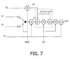
- the MIXER sample calculation means calculate a new sample OUT at from the interpolation parameters ⁇ and SIGN and signals derived from the digital signal S (RT). Derived signals are the two known basic signals LS and TS and the two filtered signals F0 and F2. The interpolation of an OUT sample is done between the two signals of base LS and TS and takes place as follows.
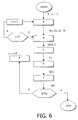
- the flowchart in Figure 6 shows the different stages presented below.
- phase parameter ⁇ is initialized preferably at -1 in order to calibrate on the first basic sample TS.
- a first step A the first filtered reference signal F0 and the second filtered signal F2 thanks to the second FIRA filtering means of FIG. 4, as previously described.
- n is an integer. also retrieves the basic signals LS, TS.
- a second step B the interpolation parameters ⁇ and SIGN are calculated according to (2).
- F1 (nearest sample - F0)
- a sixth step F the phase parameter ⁇ is incremented by a ratio R.
- step B the steps are repeated from step B) for a new OUT sample.
- phase parameter ⁇ becomes positive, the said parameter is decremented by 1 and we repeat the previous steps from step A) for a new sample OUT. Decrement allows you to readjust for interpolation on the samples of known base TS and LS, because the samples in the delay line have been shifted by a period YOUR.
- Said R ratio can take any real value. This effectively flexible management of said symbol frequencies.
- the MOD modulation means make it possible to modulate the signal thus oversampled on the carrier frequency Fca. Thereafter, said signal is sent to the CHA channel.
- the sampled signal can be shifted in time by initializing, using the digital control oscillator NCO, the phase parameter ⁇ to a value greater than or less than -1.
- the DM digital modulator preferably comprises synchronization means for appropriate signals (not shown) for performing said synchronization.
- these means are queues that store signals while waiting for the means following read them, or again, these means are control signals which inform that a signal is available or a signal is read. So each of the means sends a new output signal as soon as the current output signal is used by the following means and that an input signal is available from the above means.
- the invention described has the advantage of no longer making the symbol frequency Fsy depend on the clock frequency Fclk.
- the invention has another advantage which is to be able to freely choose its symbol frequency Fsy, whatever the clock frequency used Fclk. This makes it possible to optimize the use of the bandwidth of the channel in particular when there are several transmitting sources. Indeed, if we have a channel for which we use a carrier frequency between 5.5 MHz and 8.5 MHz and symbol frequencies of about 1 MHz, and if there are four sources that share this channel, then each uses the channel in the respective intervals of [5 MHz, 6 MHz], [6 MHz, 7 MHz], [7 MHz, 8 MHz], and [8 MHz, 9 MHz].
- the device according to the present invention has the advantage of not being expensive and less complex in comparison with a device which would include several oscillators making it possible to manage different symbol frequencies.
- H (Z) Z - ⁇ / 2 expressing said delay ⁇ T.
- H ( ⁇ ) cos ( ⁇ / 2) - j.sin (- ⁇ / 2).
- the scope of the invention is in no way limited to the embodiment described and extends to other embodiments in which, for example, the second FIRA filtering means of the interpolation means INT have a structure with three multiplying coefficients C L 1, C L 2 and C L 3 for the filtered signal of reference F0, of respective values 39/64, -9/64 and 2/64.
- Such a digital modulator can be used in particular in a decoding box commonly called in the English language “set top box” or in a modem cable.
- the invention is in no way limited to the field of television by cable, it can be extended to other fields, in particular to all those who use a digital modulator, such as the satellite domain or the transmission domain earthly.
Landscapes
- Engineering & Computer Science (AREA)
- Physics & Mathematics (AREA)
- Computer Hardware Design (AREA)
- Mathematical Physics (AREA)
- Computer Networks & Wireless Communication (AREA)
- Signal Processing (AREA)
- Digital Transmission Methods That Use Modulated Carrier Waves (AREA)
Abstract
Description
Elle trouve une application particulière notamment lors de transmissions de signaux numériques via des supports filaires tels que le câble, aériens tels que les faisceaux hertziens ou encore optiques tels que les fibres optiques.
Bien que cet état de la technique permette de gérer plusieurs fréquences symboles, cette gestion est d'autant plus complexe qu'il y a de fréquences symboles utilisées. De plus, ce système est peu flexible puisqu'il ne permet pas une utilisation continue de la gamme des fréquences symboles.
- des moyens d'interpolation aptes à interpoler un nouvel échantillon à partir de paramètres d'interpolation et de signaux dérivés du signal numérique, des paramètres d'interpolation étant calculés en fonction d'un ratio variable et réel proportionnel à la fréquence symbole sur la fréquence d'horloge.
- calculer des paramètres d'interpolation,
- calculer un nouvel échantillon à partir des paramètres d'interpolation et de signaux dérivés du signal numérique, des paramètres d'interpolation étant calculés en fonction d'un ratio variable et réel proportionnel à la fréquence symbole sur la fréquence d'horloge.
- la Fig. 1 illustre de façon schématique une architecture de modulateur numérique selon l'invention,
- la Fig. 2 est un schéma de symboles gérés par le modulateur de la figure 1,
- la Fig. 3 un schéma de moyens d'interpolation compris dans le modulateur de la figure 1,
- la Fig. 4 illustre de façon schématique une première partie des moyens d'interpolation de la figure 3,
- la Fig. 5 représente des courbes relatives à des paramètres des moyens d'interpolation de la figure 3,
- la Fig. 6 représente un organigramme de calcul effectué par les moyens d'interpolation de la figure 3,
- la Fig. 7 illustre de façon schématique une deuxième partie des moyens d'interpolation de la figure 3.
| I | Q | SYMB |
| 0 | 0 | -1 -1 |
| 0 | 1 | -1 1 |
| 1 | 1 | 1 1 |
| 1 | 0 | 1 -1 |
H(Z) = Z -∂/2 exprimant ledit retard ΔT. On a ΔT = ∂*TA/2 avec ∂ = -1,...,1.. ∂ exprime un délai normalisé par rapport à TA/2.
- des deuxièmes moyens de filtrage FIRA;
- des moyens de contrôle CNTRL,
- des moyens de calcul d'échantillons MIXER.

L'invention présente un autre avantage qui est de pouvoir choisir librement sa fréquence symbole Fsy, quelle que soit la fréquence d'horloge utilisée Fclk. Cela permet d'optimiser l'utilisation de la bande passante du canal en particulier lorsqu'il existe plusieurs sources émettrices. En effet, si on a un canal pour lequel on utilise une fréquence porteuse entre 5.5 MHz et 8.5 MHz et des fréquences symboles de 1 MHz environ, et s'il existe quatre sources qui se partagent ce canal, alors chacune utilise le canal dans les intervalles respectifs de [5 MHz, 6 MHz], [6 MHz, 7 MHz], [7 MHz, 8 MHz], et [8 MHz, 9 MHz]. Quand il existe du bruit sur une partie du canal, entre 7.9 MHz et 8.4 MHz, on peut, grâce à l'invention, choisir deux autres fréquences symboles de 0,6 MHz et 0,9 MHz, au facteur de retombée près, de telle manière que le canal soit utilisé dans les intervalles [5 MHz, 6 MHz], [6 MHz, 7 MHz], [7 MHz, 7.9 MHz], et enfin [8,4 MHz, 9 MHz]. Auparavant, on aurait eut une répartition des sources sur le canal de la manière suivante : [5 MHz, 6 MHz], [6 MHz, 7 MHz] uniquement pour deux sources. Une partie du canal entre 7 MHz et 8.4 MHz aurait été inutilisée, bien qu'utilisable. On notera également, que le dispositif selon la présente invention présente l'avantage de ne pas être coûteux et moins complexe par comparaison avec un dispositif qui comporterait plusieurs oscillateurs permettant de gérer différentes fréquences symboles.
Nous allons maintenant expliquer en quoi la fonction G(∂) correspond à une fonction de transfert H(Z) = Z-∂/2 exprimant ledit retard ΔT. On a Z = ej avec = ω*TA une fréquence radiale.
On obtient H(ej) = e-j∂/2 avec une amplitude de 1 et une phase de = -∂/2.
En terme complexe, on a H() = cos(∂/2) - j.sin(-∂/2). A ∂ = 0, on prend un échantillon courant comme référence. Afin de calculer un échantillon désiré H(Z), on utilise des moyens de filtrage FIRA qui en créant un retard d'une demi-période TA/2 permettent d'obtenir un premier signal filtré F0, et on calcule ce qu'on doit ajouter (G(Z)) à un échantillon le plus proche (1). On obtient une fonction de différentiation G(Z) ou terme de correction tel que
Ce qui équivaut à
L'équation (5) est réécrite de la manière suivante.
G(,∂) = ∂.[(/2).(sin(∂./4)/(∂./4)).- j.e-j∂/4].
Pour ∂ ≅ 1, le terme entre crochet s'écrit F1 = j. 2sin(/4).e-j/4 et
pour ∂ ≅ 0 avec (sin(∂./4)/(∂./4)) ≅ 1, le terme entre crochet s'écrit F2 = -j. /2.
Ainsi, la fonction G(,∂) peut s'écrire G(,∂) = ∂.[k1(∂).F1+k2(∂).F2] + Fe où k1 et k2 sont des facteurs appropriés et Fe est un terme d'approximation. On définit le premier signal filtré F0 pour ∂ = 1 tel que F0 = e-j/2. Ainsi, F1 = F0 -1 d'après la relation (4).
On fait une approximation telle que Fe = 0 et k1 et k2 fonctions linéaires de ∂.
On prend k1 = ∂ et k2 = 1- ∂ et on obtient G(∂) = ∂[∂.F1+(1-∂).F2] (6).
Jusqu'à maintenant, on a pris l'échantillon courant comme référence à ∂ = 0. Dans ce cas, lorsque ∂ change de signe, pour calculer des échantillons désirés, il est nécessaire d'ajouter un retard supplémentaire et on doit recalculer le premier signal filtré F0 et par suite F1. La relation 6 n'est donc valable que sur un domaine restreint de ∂, soit 0,...,1 ou -1,..., 0. Pour cette raison, il est plus simple de prendre le premier signal filtré F0 comme échantillon de référence pour calculer les échantillons désirés. Dans ce cas, lorsque ∂ change de signe, ce sont les échantillons non filtrés plutôt que les échantillons filtrés qui doivent être décalés d'une période TA. Ainsi, on n'a pas besoin d'ajouter un retard supplémentaire car les échantillons non filtrés de base LS et TS peuvent être déduits directement de la ligne à retard d'où est issu le signal de référence filtré F0. Seul le délai ∂ doit être modifié en prenant sa valeur complémentaire δ qui correspond au premier paramètre d'interpolation vu précédemment. Les figures 5a et 5b montrent les relations entre les échantillons de base LS et TS, l'échantillon de référence F0 et un échantillon désiré OUT.
Une conséquence est que le signal F1 doit être calculé tel que F1 = échantillon le plus proche - F0 plutôt que F1 = F0 - échantillon le plus proche car on a décalé le signal de référence d'une demi-période TA/2.
On obtient donc la fonction de différentiation G(δ) = |δ|(|δ|.F1 + (1-|δ|).SIGN.F2).
Claims (8)
- Modulateur numérique (DM) comportant une fréquence d'horloge (Fclk) et étant apte à traiter un signal numérique (S(TA)) comprenant des symboles (SYMB) échantillonnés à une fréquence symbole (Fsy), caractérisé en ce qu'il comporte :des moyens d'interpolation (INT) aptes à interpoler un nouvel échantillon (OUT) à partir de paramètres d'interpolation (δ, SIGN) et de signaux (LS, TS, F0, F2) dérivés du signal numérique (S(TA)), des paramètres d'interpolation (δ, SIGN) étant calculés en fonction d'un ratio (R) variable et réel proportionnel à la fréquence symbole (Fsy) sur la fréquence d'horloge (Fclk).
- Modulateur numérique selon la revendication 1, caractérisé en ce que les moyens d'interpolation (INT) comportent des moyens de filtrage (FIRA) aptes à obtenir, à partir du signal numérique (S(TA)), les signaux dérivés comprenant des signaux de base (LS, TS) et des signaux filtrés (F0, F2), et des moyens de contrôle (CNTRL) aptes à fournir lesdits paramètres d'interpolation (δ, SIGN).
- Modulateur numérique selon la revendication 1, caractérisé en ce qu'il comporte un oscillateur (NCO) apte à initialiser un paramètre de phase (µ), ledit paramètre permettant de calculer lesdits paramètres d'interpolation (δ, SIGN) en fonction dudit ratio (R).
- Procédé de traitement de signal numérique (S(TA)) comprenant des symboles (SYMB) échantillonnés à une fréquence symbole (Fsy), caractérisé en ce qu'il comporte les étapes de :calculer des paramètres d'interpolation (δ, SIGN),calculer un nouvel échantillon (OUT) à partir des paramètres d'interpolation (δ, SIGN) et de signaux (LS, TS, F0, F2) dérivés du signal numérique (S(TA)), des paramètres d'interpolation (δ, SIGN) étant calculés en fonction d'un ratio (R) variable et réel proportionnel à la fréquence symbole (Fsy) sur la fréquence d'horloge (Fclk).
- Procédé de traitement de signal selon la revendication 4, caractérisé en ce que l'étape de retarder le signal comporte une sous-étape supplémentaire de :filtrer le signal numérique (S(TA)) pour obtenir les signaux dérivés comprenant des signaux de base (LS, TS) et des signaux filtrés (F0, F2).
- Procédé de traitement de signal selon la revendication 4, caractérisé en ce qu'il comporte une étape supplémentaire d'initialiser un paramètre de phase (µ), ledit paramètre permettant de calculer lesdits paramètres d'interpolation (δ, SIGN) en fonction dudit ratio (R).
- Boítier de décodage comprenant un modulateur numérique tel que revendiqué dans l'une des revendications 1 à 3.
- Modem câble comprenant un modulateur numérique tel que revendiqué dans l'une des revendications 1 à 3.
Applications Claiming Priority (2)
| Application Number | Priority Date | Filing Date | Title |
|---|---|---|---|
| FR0103413A FR2822322A1 (fr) | 2001-03-13 | 2001-03-13 | Modulateur numerique |
| FR0103413 | 2001-03-13 |
Publications (1)
| Publication Number | Publication Date |
|---|---|
| EP1241784A1 true EP1241784A1 (fr) | 2002-09-18 |
Family
ID=8861072
Family Applications (1)
| Application Number | Title | Priority Date | Filing Date |
|---|---|---|---|
| EP02075834A Withdrawn EP1241784A1 (fr) | 2001-03-13 | 2002-03-04 | Modulateur numerique |
Country Status (6)
| Country | Link |
|---|---|
| US (1) | US6993089B2 (fr) |
| EP (1) | EP1241784A1 (fr) |
| JP (1) | JP4014898B2 (fr) |
| KR (1) | KR100910885B1 (fr) |
| CN (1) | CN1254063C (fr) |
| FR (1) | FR2822322A1 (fr) |
Families Citing this family (1)
| Publication number | Priority date | Publication date | Assignee | Title |
|---|---|---|---|---|
| JP4598587B2 (ja) | 2005-04-08 | 2010-12-15 | パナソニック株式会社 | デジタル変調装置及びデジタル変調方法 |
Citations (1)
| Publication number | Priority date | Publication date | Assignee | Title |
|---|---|---|---|---|
| US5349548A (en) * | 1992-06-26 | 1994-09-20 | U.S. Philips Corporation | Non-integral delay circuit |
Family Cites Families (10)
| Publication number | Priority date | Publication date | Assignee | Title |
|---|---|---|---|---|
| EP0093219B1 (fr) * | 1982-04-30 | 1986-04-02 | International Business Machines Corporation | Procédé de codage numérique et dispositif de mise en oeuvre dudit procédé |
| FR2753590B1 (fr) | 1996-09-19 | 1998-10-30 | Org Europeenne Telecommunications Par Satellite Eutelsat | Dispositif d'emission d'informations numeriques par satellite |
| US5764113A (en) * | 1997-01-10 | 1998-06-09 | Harris Corporation | Re-sampling circuit and modulator using same |
| US6169767B1 (en) * | 1997-03-10 | 2001-01-02 | Sarnoff Corporation | Universal network interface module |
| US6421396B1 (en) * | 1997-04-16 | 2002-07-16 | Broadcom Corporation | Variable rate modulator |
| US6140822A (en) * | 1997-05-29 | 2000-10-31 | Williams; Thomas H. | System for signal path characterization with a reference signal using stepped-frequency increments |
| US6031431A (en) | 1997-11-07 | 2000-02-29 | Hitachi America, Ltd. | Methods and apparatus for implementing modulators and programmable filters |
| US6128357A (en) * | 1997-12-24 | 2000-10-03 | Mitsubishi Electric Information Technology Center America, Inc (Ita) | Data receiver having variable rate symbol timing recovery with non-synchronized sampling |
| US6563862B1 (en) * | 1998-10-21 | 2003-05-13 | Thomson Licensing Sa | Digital variable symbol rate modulation |
| US6545532B1 (en) * | 1999-09-08 | 2003-04-08 | Atmel Corporation | Timing recovery circuit in a QAM demodulator |
-
2001
- 2001-03-13 FR FR0103413A patent/FR2822322A1/fr active Pending
-
2002
- 2002-03-04 EP EP02075834A patent/EP1241784A1/fr not_active Withdrawn
- 2002-03-09 CN CNB021056579A patent/CN1254063C/zh not_active Expired - Fee Related
- 2002-03-09 KR KR1020020012682A patent/KR100910885B1/ko not_active Expired - Fee Related
- 2002-03-11 JP JP2002064710A patent/JP4014898B2/ja not_active Expired - Fee Related
- 2002-03-12 US US10/095,509 patent/US6993089B2/en not_active Expired - Fee Related
Patent Citations (1)
| Publication number | Priority date | Publication date | Assignee | Title |
|---|---|---|---|---|
| US5349548A (en) * | 1992-06-26 | 1994-09-20 | U.S. Philips Corporation | Non-integral delay circuit |
Non-Patent Citations (1)
| Title |
|---|
| KYUNG-HO CHO ET AL: "A VLSI architecture for a frequency-agile single-chip 10-MBAUD digital QAM modulator", 1999. GLOBECOM, vol. 1a, 5 December 1999 (1999-12-05) - 9 December 1999 (1999-12-09), pages 168 - 172, XP010373292 * |
Also Published As
| Publication number | Publication date |
|---|---|
| KR20020073259A (ko) | 2002-09-23 |
| US20020181570A1 (en) | 2002-12-05 |
| JP4014898B2 (ja) | 2007-11-28 |
| US6993089B2 (en) | 2006-01-31 |
| KR100910885B1 (ko) | 2009-08-05 |
| FR2822322A1 (fr) | 2002-09-20 |
| CN1254063C (zh) | 2006-04-26 |
| CN1375970A (zh) | 2002-10-23 |
| JP2002335293A (ja) | 2002-11-22 |
Similar Documents
| Publication | Publication Date | Title |
|---|---|---|
| EP0580216B1 (fr) | Système et récepteur de signaux à répartition multiplexée de fréquences orthogonales muni d'un dispositif de synchronisation de fréquences | |
| EP0798902A1 (fr) | Estimateur et récupérateur de phase robuste pour signaux numériques affectés notamment de gigue de phase | |
| EP0797884A1 (fr) | Procede pour equilibrer les voies d'un amplificateur de type "linc" | |
| FR2896109A1 (fr) | Dispositif de conversion analogique numerique a entrelacement temporel et a egalisation auto adaptative. | |
| FR2736231A1 (fr) | Systeme de communication numerique comportant un recepteur dote d'un dispositif de recuperation de rythme | |
| WO2010146301A1 (fr) | Procedes d'emission et de reception d'un signal multiporteuse mettant en oeuvre des filtres prototypes, dispositifs d'emission et de reception, signal et programme d'ordinateur correspondants | |
| EP2854354B1 (fr) | Procédé de détermination des imperfections d'une voie d'émission et d'une voie de réception d'un équipement et équipement associé | |
| EP1473896A1 (fr) | Procédé de configuration d'un modem xDSL et modem xDSL disposant d'un tel procédé | |
| EP1039628A1 (fr) | Emetteur radiofréquence à fort degré d'intégration et avec annulation d'image, éventuellement auto-calibrée | |
| FR2822322A1 (fr) | Modulateur numerique | |
| EP0461022B1 (fr) | Dispositif de récupération d'une onde porteuse muni d'un moyen d'inhibition de faux accrochages en fréquence | |
| EP1675338A1 (fr) | Dispositif de conversion analogique-numérique avec circuit de décision et seuil de décision optimisé | |
| FR2885471A1 (fr) | Procede de decodage iteratif d'un signal ofdm/oqam utilisant des symboles a valeurs complexes, dispositif et programme d'ordinateur correspondants | |
| EP1655882A1 (fr) | Dispositif de fourniture d'un signal d'erreur pour une boucle de correction de cadence d'un démodulateur numérique | |
| EP2351305B1 (fr) | Procédé de modulation multi-états à phase continue et émetteur mettant en oeuvre le procédé | |
| WO2021099071A1 (fr) | Procédé de traitement d'un signal mis en œuvre par un dispositif de réception d'un premier site de diffusion pour supprimer un signal interférent, dispositif de réception et programme d'ordinateur correspondants. | |
| WO2006032768A1 (fr) | Procede d'estimation de la phase et du gain de donnees d'observation transmises sur un canal de transmission en modulation qam | |
| EP0786887A1 (fr) | Procédé de compensation des différences en temps de propagation de groupe entre les filtres analogiques d'un émetteur ou d'un récepteur de signaux en quadrature de phase | |
| EP0070236B1 (fr) | Dispositif de compensation de phase d'écho et son application aux annuleurs d'écho | |
| EP0335797A1 (fr) | Procédé et dispositif de synchronisation en réception d'une horloge locale d'une station d'un réseau de communication, notamment d'un véhicule automobile | |
| WO2000014937A1 (fr) | Procede et dispositif de recuperation de porteuse d'un signal numerique | |
| EP1826973A1 (fr) | Procédé et dispositif d'estimation de la fonction de transfert du canal de transmission pour démodulateur COFDM | |
| EP0850521A1 (fr) | Recuperation d'horloge pour recepteur d'un systeme de transmission synchrone | |
| EP1315347B1 (fr) | Procédé et dispositif d'égalisation utilisant des signaux probes | |
| FR2598868A1 (fr) | Procede et dispositif de recuperation du rythme et de la phase d'un signal numerique, utilisant la derivee du signal, et systeme de reception de ce signal utilisant le dispositif |
Legal Events
| Date | Code | Title | Description |
|---|---|---|---|
| PUAI | Public reference made under article 153(3) epc to a published international application that has entered the european phase |
Free format text: ORIGINAL CODE: 0009012 |
|
| AK | Designated contracting states |
Kind code of ref document: A1 Designated state(s): AT BE CH CY DE DK ES FI FR GB GR IE IT LI LU MC NL PT SE TR |
|
| AX | Request for extension of the european patent |
Free format text: AL;LT;LV;MK;RO;SI |
|
| 17P | Request for examination filed |
Effective date: 20030318 |
|
| AKX | Designation fees paid |
Designated state(s): AT BE CH CY DE DK ES FI FR GB GR IE IT LI LU MC NL PT SE TR |
|
| RAP1 | Party data changed (applicant data changed or rights of an application transferred) |
Owner name: NXP B.V. |
|
| STAA | Information on the status of an ep patent application or granted ep patent |
Free format text: STATUS: THE APPLICATION IS DEEMED TO BE WITHDRAWN |
|
| 18D | Application deemed to be withdrawn |
Effective date: 20100302 |