EP1241677A1 - Semiconductor device using non-volatile memory in which data is written circularly - Google Patents
Semiconductor device using non-volatile memory in which data is written circularly Download PDFInfo
- Publication number
- EP1241677A1 EP1241677A1 EP02005757A EP02005757A EP1241677A1 EP 1241677 A1 EP1241677 A1 EP 1241677A1 EP 02005757 A EP02005757 A EP 02005757A EP 02005757 A EP02005757 A EP 02005757A EP 1241677 A1 EP1241677 A1 EP 1241677A1
- Authority
- EP
- European Patent Office
- Prior art keywords
- data
- region
- memory
- written
- latest data
- Prior art date
- Legal status (The legal status is an assumption and is not a legal conclusion. Google has not performed a legal analysis and makes no representation as to the accuracy of the status listed.)
- Granted
Links
- 230000015654 memory Effects 0.000 title claims abstract description 379
- 239000004065 semiconductor Substances 0.000 title claims abstract description 67
- 238000000034 method Methods 0.000 claims description 68
- 101100087530 Caenorhabditis elegans rom-1 gene Proteins 0.000 description 5
- 101100305983 Mus musculus Rom1 gene Proteins 0.000 description 5
- 238000013500 data storage Methods 0.000 description 3
- 238000010586 diagram Methods 0.000 description 2
- 230000004048 modification Effects 0.000 description 2
- 238000012986 modification Methods 0.000 description 2
- 235000013365 dairy product Nutrition 0.000 description 1
- 230000004044 response Effects 0.000 description 1
Images





Classifications
-
- G—PHYSICS
- G11—INFORMATION STORAGE
- G11C—STATIC STORES
- G11C16/00—Erasable programmable read-only memories
- G11C16/02—Erasable programmable read-only memories electrically programmable
- G11C16/06—Auxiliary circuits, e.g. for writing into memory
- G11C16/34—Determination of programming status, e.g. threshold voltage, overprogramming or underprogramming, retention
- G11C16/349—Arrangements for evaluating degradation, retention or wearout, e.g. by counting erase cycles
-
- G—PHYSICS
- G11—INFORMATION STORAGE
- G11C—STATIC STORES
- G11C16/00—Erasable programmable read-only memories
- G11C16/02—Erasable programmable read-only memories electrically programmable
- G11C16/06—Auxiliary circuits, e.g. for writing into memory
- G11C16/10—Programming or data input circuits
- G11C16/102—External programming circuits, e.g. EPROM programmers; In-circuit programming or reprogramming; EPROM emulators
Definitions
- the present invention relates to a semiconductor device. More particularly, the present invention relates to a semiconductor device having a built-in non-volatile memory in which a permissive number of times of rewrite is limited.
- Non-volatile memories are known such as EEPROM (Electrically Erasable Programmable Read Only Memory), a flash memory and FeRAM (Ferroelectric Random Access Memory).
- the non-volatile memory which can hold data without any power supply is suitable for a data memory for an IC card.
- the permissive number of times of rewrite is presently limited.
- the permissive number of times of rewrite of the EEPRO is limited to about 10 5
- the permissive number of times of rewrite of the flash memory is limited to about 10 4
- the permissive number of times of rewrite of the FeRAM is limited to about 10 10 .
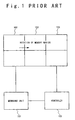
- FIG. 1 shows a conventional memory device to which the conventional data managing method is applied.
- the memory is limited in the permissive number of times of rewrite, and has a managing unit 101, a controller 102 and a plurality of memory regions 103.
- the managing unit 101 manages the number of times of rewrite of each memory region 103.
- the controller 102 selects one for data to be written from the memory regions 103 based on the permissive number of times of rewrite of each memory region 103.
- the controller 102 compares the numbers of times of rewrite of the memory regions 103, and selects the memory region with the minimum number of time of rewrite.
- the rewriting operation is carried out to the memory region with the minimum number of times of rewrite.
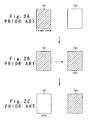
- Figs. 2A to 2C show an operation of the conventional memory device in which the permissive number of times of rewrite is limited. It is supposed that a first semiconductor chip as a first memory region 103 1 of the memory regions 103 is already rewritten five times and a second semiconductor chip as a second memory region 103 2 of the memory regions 103 is not yet used. The number of times of rewrite of the first memory chip 103 1 and that of rewrite of the second memory chip 103 2 are compared with each other, and the second memory chip 103 2 with the smaller number of times is smaller is selected as a memory chip for the data to be rewritten. Contents of the first memory chip 103 1 are copied to the second memory chip 103 2 .
- the second memory chip 103 2 is used.
- the first memory chip 103 1 is collectively erased in units of chips.
- the first memory chip 103 1 is not used until the number of times of rewrite of the second memory chip 103 2 exceeds that of rewrite of the first memory chip 103 1 .
- the change of the memory chip 103 to be used is carried out so as to always use the memory chip with the minimum number of times of rewrite from among the plurality of memory chips 103.
- the memory chips 103 are accessed in the same number of times. If the number of the memory chips 103 is N, the lifetime of the memory chips 103 is elongated to N times.
- JP-A-Heisei 9-265427 a write method of a rewitable ROM is disclosed in Japanese Laid Open Patent application (JP-A-Heisei 9-265427).
- the data region of the ROM is divided into blocks with a predetermined block length. Each of the blocks is allocated with an address.
- a CPU specifies one of the blocks based on a block address and data and writes a file in units of blocks. At this time, the CPU writes the file from an empty block when there is the empty block with a write start mark and from an optimal empty block when there is no empty block with the mark. After completion of the write of the file, the CPU searches an empty block in a downstream direction and writes the write start mark in the searched empty block.
- a semiconductor memory device is disclosed in Japanese Laid Open Patent application (JP-A-Heisei 8-96588).
- the memory device is of a non-volatile type.
- a data storage section has at least one block, which can be independently written and erased, in a data storage region of the non-volatile memories.
- a block selecting section calculates a physical address from a logical address to specify one of the blocks.
- a search section searches an unused block from the data storage section.
- An erasure managing section manages initial erasure of the blocks. Data is written in the selected block and the block selecting section specifies the searched block as an object.
- non-volatile memory it is desirable that the data stored in the non-volatile memory is not damaged even if the power supply to the non-volatile memory is interrupted during the access to the non-volatile memory.
- the non-volatile memory is used as a data memory for an IC card, the sudden interruption of the power supply is assumed to be frequently brought about. For example, if the non-volatile memory is used in a contact type IC card, the contact type IC card may be suddenly pulled out from a power supply terminal by a user.
- a non-contact type IC card to which power is supplied with electric wave is separated from a transmitter of the electric wave, there may be a case that a necessary power supply voltage cannot be kept.
- the interruption of the power supply is assumed to be brought about during the access to the non-volatile memory. If the non-volatile memory is used as the data memory for the IC card, it is important that the data stored in the non-volatile memory is not damaged even if the power supply is interrupted.
- an object of the present invention is to provide the technique for fictionally extending the lifetime of the non-volatile memory in which the permissive number of times of rewrite is limited.
- Another object of the present invention is to provide the technique for simply determining a memory region to be used for rewrite and performing the rotation on the memory region, and thereby fictionally extending the lifetime of the non-volatile memory in which the permissive number of times of rewrite is limited.
- Still another object of the present invention is to provide the technique for reducing the risk that the data stored in the non-volatile memory is damaged if the power supply to the non-volatile memory is interrupted during the access to the non-volatile memory.
- Yet still another object of the present invention is to provide the technique for detecting the interruption of the power supply to the non-volatile memory if the power supply to the non-volatile memory is interrupted.
- a semiconductor device includes a non-volatile memory and a control unit which reserves n memory regions (n is an integer equal to or more than 2) for n of data as first to n-th memory regions in the non-volatile memory and writes the data in the first memory region, when the data is written in the non-volatile memory.
- the control unit sequentially and circularly writes the updated data as the latest data in the n memory regions, and each time the data is updated.
- the control unit may reserve a pointer region in the non-volatile memory to indicate an i-th one (i is an integer between 1 and n) of the first to n-th memory regions in which the latest data is written.
- the control unit may refer to the pointer region to read out the latest data from the i-th memory region.
- the pointer region may include (n-1) bit regions for the n memory regions. It is desirable that a (j-1)-th bit region (j is an integer between 2 and n) of the (n-1) bit regions indicates the j-th memory region in which the latest data has been written.
- the control unit may change a value of the (j-1)-th bit region from a first value to a second value when the latest data is written in the j-th memory region. Also, the control unit may reset values of the (n-1) bit regions to the first value when the latest data is written in the first memory region.
- the pointer region may include n bit regions corresponding to the n memory regions, and an i-th bit region of the n bit regions indicates the i-th memory region in which the latest data has been written.
- the control unit may change a value of the i-th bit region from a first value to a second value and changes a value of the (i-1)-th bit region from the second value to the first value.
- control unit may reserve a power failure check region in the non-volatile memory.
- the power failure check region indicates whether power failure has occurred before the latest data is written in the i-th memory region.
- the control unit may refer to the pointer region and the power failure check region to determine an (i-1)-th memory region if the power failure check region indicates that the power failure has occurred when the latest data is written in the i-th memory region and the i-th memory region if the power failure check region indicates no power failure when the latest data is written in the i-th memory region.
- control unit may read out the latest data from the determined memory region, and writes the updated data as the latest data in the memory region next to the determined memory region.
- control unit may determine n based on information supplied to the control unit.
- the above semiconductor device may be used for an IC card.
- a method of writing and updating data in a non-volatile memory may be achieved by (a) reserving n memory regions (n is an integer equal to or more than 2) for n of data as first to n-th memory regions in a non-volatile memory, when the data is written in the non-volatile memory; by (b) reserving a pointer region in the non-volatile memory, the pointer region indicating that the latest data is written an i-th one (i is an integer between 1 and n) of the first to n-th memory regions; by (c) writing the data in the first memory region as the latest data; by (d) sequentially and circularly writing the latest data in the n memory regions while the i increments by one each time the latest data is updated and the updated data is written as the latest data; and by (e) updating the pointer region to indicate that the latest data has been written in the i-th memory region, when the latest data has been written in the i-th
- the (d) sequentially and circularly writing step may be achieved by (f) referring to the pointer region to determine the i-th memory region, when the latest data is updated; by (g) reading out the latest data from the i-th memory region; and by (h) writing the updated data as the latest data in an (i+1)-th memory region.
- the pointer region may include (n-1) bit regions for the n memory regions.
- the (e) updating step may be achieved by changing a value of the (j-1)-th bit region from a first value to a second value when the latest data is written in the j-th memory region.
- the (e) updating step may further include resetting values of the (n-1) bit regions to the first value when the latest data is written in the first memory region.
- the pointer region may include n bit regions corresponding to the n memory regions.
- the (e) updating step may be achieved by changing a value of the i-th bit region from a first value to a second value and changes a value of the (i-1)-th bit region from the second value to the first value, when the latest data is read out from an (i-1)-th memory region, updated and written in the i-th memory region.
- the method may further include (i) reserving a power failure check region in the non-volatile memory.
- the (d) sequentially and circularly writing step further includes, when the latest data written in the i-th memory region should be further updated, referring to the pointer region and the power failure check region to determine an (i-1)-th memory region if the power failure check region indicates that the power failure has occurred when the latest data is written in the i-th memory region and the i-th memory region if the power failure check region indicates no power failure when the latest data is written in the i-th memory region; reading out the latest data from the determined memory region; and writing the updated data as the latest data in the memory region next to the determined memory region.
- the (a) reserving step may include determining the n based on given information.
- the above method may be achieved based on a program.
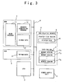
- Fig. 3 shows a semiconductor device according to the first embodiment of the present invention.
- the semiconductor device is used for an IC card.
- the semiconductor device includes a ROM 1, a CPU 2, a RAM 3, a non-volatile memory 4 and a power supply unit 5.
- the ROM 1, the CPU 2, the RAM 3 and the non-volatile memory 4 are connected to each other through a bus 6.
- Power is supplied from the power supply unit 5 through a power supply line (not shown) to the ROM 1, the CPU 2, the RAM 3 and the non-volatile memory 4.
- a power supply unit 5 for converting a power supply voltage supplied from an external portion into a power supply voltage to be used in the semiconductor device is selected as the power supply unit 5.
- the ROM 1 stores therein a main program 11, an address conversion program 12 and in-ROM data 13.
- the main program 11 describes the whole operation of an IC card.
- the semiconductor device is operated in accordance with the main program 11.
- the address conversion program 12 is a program for converting a virtual or logical address into a physical address.
- the logical address is used to specify an address if an access to a memory space is carried out.
- the logical address is converted into the physical address using the address conversion program 12.
- the access is actually carried out to a region of the ROM 1, the RAM 2 and the non-volatile memory 4 which are specified by the physical address.
- the in-ROM data 13 contains only data to be read out, of the data used in the main program 11.
- the CPU 2 executes the main program 11 and the address conversion program 12, and then controls the whole operation of the semiconductor device of the present invention.
- the RAM 3 stores therein in-RAM data 31.
- the in-RAM data 31 contains the data on which a re-written operation is frequently performed, of the data used in the main program 11.
- the data which needs to be stored in the non-volatile manner and needs to be re-written are written to the non-volatile memory 4.
- the data are used in the main program 11.
- the main program 11 it is supposed that data is stored in a logical address X. If the logical address X specifies a region of the non-volatile memory 4, and the region of the non-volatile memory 4 is assigned to store the data of the logical address X.
- the region assigned to store the data used in the main program 11 is hereafter referred to as the data region 7.
- a plurality of data are used in the main program 11, a plurality of data region 7 are assigned in correspondence to them. However, a single data region 7 is shown in Fig. 3.
- the data region 7 is provided with a plurality of memory regions 71 1 to 71 n .
- n is an integer of 2 or more.
- the CPU 2 determines n when an instruction is inputted or information about the data such as a kind of data, and a location of the data in a data stream. However, the value of n may be fixed or predetermined.
- the CPU 2 reserves the data region 7 in the non-volatile memory 4 based on the determined value of n.
- any of the memory regions 71 1 1 to 71 n is circularly selected.
- the data to be stored in the data region 7 is written in the memory region selected from among the memory regions 71 1 to 71 n .
- the data is read out from the data region 7, the data is read out from the memory region, to which the latest writing operation is carried out, of the memory regions 71 1 to 71 n .
- a pointer flag 81 is stored in the pointer flag region 8. If a plurality of data regions 7 are provided in the non-volatile memory 4, one pointer flag 81 is provided for each data region 7.
- Fig. 3 shows only one pointer flag 81.
- the pointer flag 81 specifies one to be accessed of the memory regions 71 1 to 71 n .
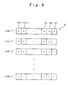
- the pointer flag 81 is provided with (n-1) bits (81 1 to 81 n-1 ) as shown in Fig. 4.
- n is the number of the memory regions 71 1 to 71 n .
- the number of bits 81 1 to 81 n-1 of the pointer flag 81 is smaller by one than the number of the memory regions 71 1 to 71 n .
- a bit 81 k of the pointer flag 81 is represented as the lower order bit as the affix k is smaller.
- the pointer flag 81 of the (n-1) bits is in either one of states 1 to n.
- the state 1 is the state in which all of the bits 81 1 to 81 n-1 are 0.
- the state 2 is the state in which the bit 811 is "1" and the remaining bits 81 2 to 81 n-1 are "0".
- the state k is the state in which the bits 81 1 to 81 k- 1 are "1" and the remaining bits 81 k to 81 n-1 are "0".
- k is an integer between 1 and n.
- the state n is the state in which all of the bits 81 1 to 81 n-1 are "1".
- a memory region to be accessed of the memory regions 71 1 to 71 n is specified based on the state of the pointer flag 81.
- the pointer flag 81 is referred by the CPU 2 using the address conversion program 12, and the memory region to be accessed of the memory regions 71 1 to 71 n is selected.
- a physical address of the selected memory region is calculated by the address conversion program 12. Then, in the non-volatile memory 4, a portion specified by the physical address is accessed.
- the correspondence between the state of the pointer flag 81 and the accessed memory region is as follows. If the pointer flag 81 is in the state 1, the data is read out from the memory region 71 1 , and the data is written to the memory region 71 2 . If the pointer flag 81 is in the state 2, the data is read out from the memory region 71 2 , and the data is written to the memory region 71 3 . Hereafter, similarly, if the pointer flag 81 is in the state k, the data is read out from the memory region 71 k , and the data is written to the memory region 71 k+1 . However, if the pointer flag 81 is in the state n, the data is written to the memory region 71 1 .
- the number n of the memory regions 71 1 to 71 n is selected such that all of the (n-1) bits 81 1 to 81 n-1 contained in the pointer flag 81 can be reset to "0" in response to one command outputted by the CPU 2. This provides the important role so that the data stored in the non-volatile memory 4 is not damaged if the power supply to the respective section of the semiconductor device from the power supply unit 5 is suddenly interrupted, as described later.
- the data region 7 is assigned to store the data of a logical address X in a memory space.
- a data to be firstly stored as the data of the logical address X is supposed to be noted as a data 1.
- the data 1 to be firstly written to the data region 7 is written to the memory region 71 1 without any condition.
- the pointer flag 81 is set in the state 1. That is, all of the bits 81 1 to 81 n-1 included in the pointer flag 81 are reset to "0".
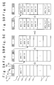
- Fig. 5A shows the states of the data region 7 and the pointer flag 81 after the completion of the process for writing the data 1.
- the CPU 2 refers to the pointer flag 81 using the address conversion program 12, and determines which of the states 1 to n the pointer flag 81 is set to. If the pointer flag 81 is determined to be in the state k (k is an integer between 1 and n), the data to be stored in the data region 7 as the data of the logical address X is written to the memory region 71 k+1 of the memory regions 71 1 to 71 n . After that, the state of the pointer flag 81 is shifted or changed from the state k to the state k+1.
- the data 1 to be firstly stored as the data of the logical address X is written to the memory region 71 1 as shown in Fig. 5A.
- the pointer flag 81 is set in the state 1.
- the address conversion program 12 refers to the pointer flag 81. At this time, the pointer flag 81 is in the state 1. Thus, as shown in Fig. 5B, the memory region 71 2 is selected as the destination to which the data 2 is written. The data 2 is written to the selected memory region 71 2 .
- Fig. 5B shows the states of the data region 7 and the pointer flag 81 after the pointer flag 81 is rewritten.
- the pointer flag 81 is sequentially shifted to the state 4, the state 5, ..., and the state n. After the completion of the process for writing the data n, the pointer flag 81 is in the state n.
- the pointer flag 81 is in the state n as shown in Fig. 5D.
- the memory region 71 1 is selected as the destination to which the data (n+1) is written.
- the data (n+1) is written to the memory region 71 1 , and the pointer flag 81 is shifted from the state n to the state 1.
- the circulation selection of the written memory regions 71 1 to 71 n enables the permissive number of times of rewrite of the data of the logical address X to be apparently greater than the permissive number of times of rewrite which is physically allowed for the non-volatile memory 4.
- Fig. 6 is a flowchart showing the writing operation to be performed on the data region 7 in detail, if the data of the logical address X is updated.
- the program for executing the operation shown in the flowchart of Fig. 6 is written in the address conversion program 12.
- the CPU 2 carries out the operation shown in the flowchart of Fig. 6, in accordance with the address conversion program 12.
- each of the bits 81 1 to 81 n-1 is at "0". The determination is carried out in turn from the lower order bit 81 1 (Step S01).
- Step S02 it is determined whether or not each of the bits 81 1 to 81 n-1 includes the bit of "0" (Step S02).
- Step S03 a value i satisfying the following condition is determined (Step S03).
- the value i indicates a position of a least significant bit for which "0" is set.
- the value i thus determined is any integer between 1 and n-1.
- the fact that the bits 81z to 81 i-1 are "1" and the remaining bits 81 i to 81 n-1 are "0" implies that the pointer flag 81 is in the state i. If the pointer flag 81 is determined to be in the state i, the memory region 71 i+1 of the memory regions 71 1 to 71 n is selected as the destination to which the data is written. The physical address of the selected memory region 71 i+1 is calculated, and the data after the update of the logical address X is written to the region indicated by the physical address of the non-volatile memory 4 (Step S03).
- Step S04 the bit 81 i+1 among the bits 81 1 to 81 n-1 is updated from "0" to "1" (Step S04).
- the pointer flag 81 is shifted from the state i to the state i+1.
- the process for updating the data of the logical address X is ended as mentioned above.
- the head memory region 71 1 of the memory regions 71 1 to 71 n is selected as the destination to which the data is written. This implies that when the pointer flag 81 is in the state n, the memory region 71 1 is selected as the destination to which the data is written.
- the physical address of the selected memory region 71 1 is calculated, and the data after the update of the logical address X is written to the region indicated by the physical address of the non-volatile memory 4 (Step S05).
- Step S06 all of the bits 81 1 to 81 n-1 contained in the pointer flag 81 are reset to "0" (Step S06).
- the bits 81 1 to 81 n-1 are collectively cleared in accordance with one command outputted from the CPU 2. If the address conversion program 12 instructs the CPU 2 to clear the bits 81 1 to 81 n-1 , the CPU 2 outputs the command to instruct the non-volatile memory 4 to clear the bits 81 1 to 81 n-1 . In accordance with the command, the non-volatile memory 4 clears all of the bits 81 1 to 81 n-1 to "0". In this way, the bits 81 1 to 81 n-1 are collectively cleared in accordance with the one command.
- Figs. 7A to 7E are diagrams showing the operation for reading out the data from the data region 7. If the data of the logical address X is read out, the address conversion program 12 firstly refers to the pointer flag 81, and determines which of the states 1 to n the pointer flag 81 is set to.
- the pointer flag 81 is determined to be in the state j (j is an integer between 1 and n) of the states 1 to n, as the data of the logical address X, the data stored in the memory region 71 j among the memory regions 71 1 to 71 n is read out. As mentioned above, immediately after the data is written to the memory region 71 j , the pointer flag 81 is updated to the state j. Thus, the data written in the memory region 71 j is the latest data of the logical address X. Since the data is read out from the memory region 71 j when the pointer flag 81 is in the state j, the latest data of the logical address X is properly read out.
- the pointer flag 81 is in the state 1. At this time, if the data of the logical address X is read out from the data region 7, the memory region 71 1 is selected as the source from which the data is read out. Then, the data of the logical address X is read out from the selected memory region 71 1 .
- the pointer flag 81 is in the state 2.
- the memory region 71 2 is selected as the source from which the data is read out, and the data of the logical address X is read out from the memory region 71 2 .
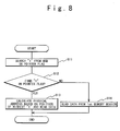
- Fig. 8 is a flowchart showing the operation for reading out the data of the logical address X from the data region 7 in detail.
- the program for executing the operation shown in the flowchart of Fig. 8 is written in the address conversion program 12.
- the CPU 2 executes the operation shown in the flowchart of Fig. 8, in accordance with the address conversion program 12.
- Step S11 it is determined whether or not each of the bits 81 1 to 81 n-1 is "1" (Step S11). The determination is carried out in turn from the high order bit 81 n-1 .
- Step S12 it is determined whether or not each of the bits 81 1 to 81 n-1 includes the bit of "1" (Step S12).
- Step S13 If any of the bits 81 1 to 81 n-1 is set “1”, j' satisfying the following condition is determined (Step S13).
- the value j' indicates the position of the most significant bit of the bits for which "1" is set.
- the bits 81 j'+1 to 81 n-1 of the bits 81 1 to 81 n-1 are "0", and the remaining bits 81 1 to 81 j , are "1".
- all of the bits 81 1 to 81 n-1 are "1"
- it is determined to be j' n-1.
- the value j' thus determined is any integer between 1 and n-1.
- the head memory region 71 1 of the memory regions 71 1 to 71 n is selected as the source from which the data is read out. This implies that when the pointer flag 81 is in the state 1, the memory region 71 1 is selected as the source from which the data is read out.
- the physical address of the selected memory region 71 1 is calculated, and the data of the logical address X is read out from the region indicated by the physical address of the non-volatile memory 4 (Step S14). The process for reading out the data of the logical address X is ended as mentioned above.
- a data region 7 is reserved for the data.
- the reserved data region 7 is comprised of the n memory regions 71 1 to 71 n (n is a natural number of 2 or more). If the data is updated and a data after the update is stored in the data region 7, one of the memory regions 71 1 to 71 n is circularly selected as the destination to which the data is written. The data is written to the selected memory region.
- the state of the pointer flag 81 is circularly shifted between the first to n-th states, in accordance with the selection of the memory regions 71 1 to 71 n .
- the respective bits 81 1 to 81 n-1 are rewritten two times during one round of the selection of the memory regions 71 1 to 71 n .
- the permissive number of times of rewrite of the non-volatile memory 4 is supposed to be N
- the state of the pointer flag 81 can be changed by [n/2] ⁇ N times.
- [x] is the maximum integer that does not exceed x.
- the data stored in the data region 7 can be updated by [n/2] ⁇ N times.
- the permissive number of times of rewrite of the data stored in the data region 7 is greater than the permissive number of times of rewrite which is physically allowed for the non-volatile memory 4.
- the risk that the data stored in the non-volatile memory 4 is damaged is small, even if the power supply to the respective section of the semiconductor device from the power supply unit 5 is suddenly interrupted during the access to the non-volatile memory 4.
- Fig. 9B it is supposed that the power supply from the power supply unit 5 is interrupted when the bit 81 i of the pointer flag 81 is updated from "0" to "1". In this case, whether the bit 81 i of the pointer flag 81 is set to "1" or "0" is determined as a probability.
- the bit 81 i of the pointer flag 81 is determined to be "0"
- this fact implies that the writing process is not normally carried out.
- the pointer flag 81 is kept in the state i.
- the data is read out from the data region 7 after that, the data is read out from the memory region 71 i . Then, the latest data is read out in which the writing process has been normally carried out.
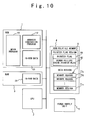
- Fig. 10 shows a semiconductor device according to the second embodiment of the present invention.
- the second embodiment differs from the semiconductor device in the first embodiment in that a power failure check pointer flag 82 is further provided in the pointer flag region 8, in addition to the pointer flag 81.
- the semiconductor device in the second embodiment uses the power failure check pointer flag 82.
- the contents of the main program 11 and the address conversion program 12 stored in the ROM 2 are modified. This modification corresponds to the fact that the power failure check pointer flag 82 is further installed in the pointer flag region 8.
- the configurations of the other portions of the semiconductor device in the second embodiment are the same as those of the semiconductor device in the first embodiment.
- Fig. 11 shows the configuration of the power failure check pointer flag 82.
- the power failure check pointer flag 82 is provided with (n-1) interruption check bits 82 1 to 82 n-1 .
- n is the number of the memory regions 71 1 to 71 n of the data region 7, as mentioned above.
- n is selected such that all of the (n-1) bits 81 1 to 81 n-1 contained in the pointer flag 81 can be collectively cleared to "0" in accordance with the one command outputted by the CPU 2.
- the (n-1) interruption check bits 82 1 to 82 n-1 contained in the power failure check pointer flag 82 can be collectively cleared to "0" in accordance with the command outputted by the CPU 2.
- the power failure check pointer flag 82 is also at any state of the states 1 to n, similarly to the pointer flag 81.
- the state 1 is the state in which all of the interruption check bits 82 1 to 82 n-1 are "0".
- the state 2 is the state at which the interruption check bit 82 1 is "1” and the remaining interruption check bits 82 2 to 82 n-1 are "0".
- the state k is the state at which the interruption check bits 82 1 to 82 k-1 are "1” and the remaining interruption check bits 82 k to 82 n-1 are "0".
- k is an integer between 1 and n.
- the state n is the state in which all of the interruption check bits 82 1 to 82 k-1 are "1".
- the pointer flag 81 and the power failure check pointer flag 82 are both kept at the same state in the usual condition. However, the interruption of the power supply during the writing process to the data region 7 causes a difference to be induced between the pointer flag 81 and the power failure check pointer flag 82. As described later, this difference enables the interruption of the power supply to be detected.
- the operation for writing a data to the data region 7 will be described.
- the data region 7 is assigned to store the data of the logical address X in the memory space.
- data to be firstly stored as the data of the logical address X is supposed to be noted as a data 1.
- the power failure check pointer flag 82 is set in the state 1. That is, all of the interruption check bits 82 1 to 82 n-1 are set to "0".
- the data 1 is written to the data region 7.
- the pointer flag 81 is set in the state 1. That is, all of the bits 81 1 to 81 n-1 included in the pointer flag 81 are set to "0".
- Fig. 12A shows the states of the data region 7, the pointer flag 81 and the power failure check pointer flag 82 after the completion of the process for writing the data 1.
- the address conversion program 12 refers to the pointer flag 81 and the power failure check pointer flag 82, and determines which of the states 1 to n each of the pointer flag 81 and the power failure check pointer flag 82 is set to.
- the pointer flag 81 and the power failure check pointer flag 82 are usually in the states coincident with each other. If the pointer flag 81 and the power failure check pointer flag 82 are determined to be in the state k (k is an integer between 1 and n), the memory region 71 k+1 of the memory regions 71 1 to 71 n is selected as a destination to which the data after the update is written.
- the power failure check pointer flag 82 is shifted from the state k to the state k+1.
- the interruption check bit 82 k of the power failure check pointer flag 82 is shifted from "0" to "1".
- the power failure check pointer flag 82 is shifted from the state n to the state 1. That is, if the pointer flag 81 and the power failure check pointer flag 82 are in the state n, all of the interruption check bits 82 1 to 82 n-1 are cleared to "0".
- the data after the update of the logical address X is written to the memory region 71 k+1 of the memory regions 71 1 to 71 n .
- the data of the logical address X is updated when the pointer flag 81 is in the state n, the data to be stored in the data region 7 as the data of the logical address X is written to the memory region 71 1 .
- the pointer flag 81 is shifted from the state k to the state k+1.
- the bit 81 k of the pointer flag 81 is shifted from "0" to "1".
- the pointer flag 81 is shifted from the state n to the state 1. That is, when the pointer flag 81 is in the state n, $81 1 to 81 n-1 are all cleared to "0".
- the data 1 to be firstly stored as the data of the logical address X is written to the memory region 71 1 as shown in Fig. 12A. Both of the pointer flag 81 and the power failure check pointer flag 82 are set in the state 1.
- the address conversion program 12 refers to the pointer flag 81 and the power failure check pointer flag 82. Both the pointer flag 81 and the power failure check pointer flag 82 are determined to be in the state 1.
- the memory region 71 2 of the memory regions 71 1 to 71 n is selected as the destination to which the data 2 is written.
- the interruption check bit 82 1 of the power failure check pointer flag 82 is updated from "0" to "1". That is, the power failure check pointer flag 82 is shifted from the state 1 to the state 2.
- Fig. 12B the interruption check bit 82 1 of the power failure check pointer flag 82 is updated from "0" to "1". That is, the power failure check pointer flag 82 is shifted from the state 1 to the state 2.
- the data 2 is written to the memory region 71 2 selected as the destination to which the data is written.
- the bit 81 1 in the pointer flag 81 is updated from "0" to "1". That is, the pointer flag 81 is shifted from the state 1 to the state 2.
- the process for writing the data 2 is ended as mentioned above.
- the power failure check pointer flag 82 is sequentially shifted to the state 3, the state 4, ..., and the state n, similarly to the above-mentioned process.
- the data 3, the data 4, ..., and the data n after the update are written to the memory region 71 4 , the memory region 71 5 , ..., the memory region 71 n .
- the pointer flag 81 is shifted sequentially to the state 3, the state 4, ..., the state n.
- the data n is written to the memory region 71 n , as shown in Fig. 13A, and the pointer flag 81 and the power failure check pointer flag 82 are in the state n.
- the pointer flag 81 and the power failure check pointer flag 82 are firstly referred.
- the pointer flag 81 and the power failure check pointer flag 82 are determined to be in the state n.
- the memory region 71 1 of the memory regions 71 1 to 71 n is selected as the destination to which the data is written.
- all of the interruption check bits 82 1 to 82 n-1 of the power failure check pointer flag 82 are cleared to "0", and the power failure check pointer flag 82 is shifted from the state n to the state 1.
- Fig. 13B all of the interruption check bits 82 1 to 82 n-1 of the power failure check pointer flag 82 are cleared to "0", and the power failure check pointer flag 82 is shifted from the state n to the state 1.
- the data (n+1) is written to the memory region 71 1 selected as the destination to which the data is written.
- Fig. 13D all of the bits 81 1 to 81 n-1 of the pointer flag 81 are cleared to "0". That is, the pointer flag 81 is shifted from the state n to the state 1.
- the process for writing the data (n+1) is ended as mentioned above.
- the address conversion program 12 firstly refers to the pointer flag 81, and determines which of the states 1 to n the pointer flag 81 is set to. At this time, the power failure check pointer flag 82 is not referred. As mentioned above, the power failure check pointer flag 82 is updated before the data is written to the memory regions 71 1 to 71 n . There is a case where the power failure check pointer flag 82 does not indicate the memory region of the memory regions 71 1 to 71 n in which latest data of the logical address X has been normally written, because the power supply is interrupted from the power supply unit 5 while the data is written to any of the memory regions 71 1 to 71 n . Thus, when the data of the logical address X is read out, the power failure check pointer flag 82 is not referred.
- the pointer flag 81 is determined to be in the state j of the states 1 to n (j is an integer between 1 and n)
- the data stored in the memory region 71 j of the memory regions 71 1 to 71 n is read out as the data of the logical address X.
- the process for reading out the data of the logical address X based on the state of the pointer flag 81 is the same as that of the first embodiment. Therefore, the detailed description is not carried out.
- the programs for executing the above-mentioned operations are written in the main program 11 and the address conversion program 12 in this embodiment.
- the CPU 2 executes the above-mentioned operations in accordance with the main program 11 and the address conversion program 12.
- the data region 7 is reserved for the data, similarly to the semiconductor device in the first embodiment.
- the reserved data region 7 is comprised of the n memory regions 71 1 to 71 n (n is a natural number of 2 or more). If the data is updated, one of the memory regions 71 1 to 71 n is circularly selected as the destination to which the data is written. The data is written to the selected memory region.
- the permissive number of times of rewrite of the data is fictionally greater than the physically permissive number of times of rewrite of the non-volatile memory 4.
- the risk that the data stored in the non-volatile memory 4 is damaged is small, even if the power supply to the respective sections of the semiconductor device from the power supply unit 5 is suddenly interrupted during the access to the non-volatile memory 4.
- the semiconductor device in this embodiment it is possible to detect the occurrence of the interruption of the power supply if the power supply from the power supply unit 5 is interrupted during the process for writing the data to the data region 7. If the power supply from the power supply unit 5 is interrupted during the update of the power failure check pointer flag 82, the write of the data to the memory regions 71 1 to 71 n and the update of the pointer flag 81, the difference is produced between the state of the pointer flag 81 and the state of the power failure check pointer flag 82. If the power supply from the power supply unit 5 is recovered, the CPU 2 determines whether or not the state of the pointer flag 81 is coincident with the state of the power failure check pointer flag 82, in accordance with the main program 11.
- the CPU 2 Since the state of the pointer flag 81 is not coincident with the state of the power failure check pointer flag 82, the CPU 2 detects the interruption of the power supply from the power supply unit 5 during the process for writing the data to the data region 7. As mentioned above, in the semiconductor device in this embodiment, it is possible to detect the occurrence of the interruption of the power supply.
- Fig. 14 shows a semiconductor device of the third embodiment according to the present invention.
- the pointer flag region 8 is not provided in the non-volatile memory 4.
- flags 72 1 to 72 n are added to the memory regions 71 1 to 71 n of the data region 7, respectively.
- Each of the flags 72 1 to 72 n stores one-bit data.
- the data region 7 to which the flags 72 1 to 72 n are added is hereafter referred as a data region 7'.
- the whole of the flags 72 1 to 72 n is referred to as a flag set 72.
- the contents of the main program 11 and the address conversion program 12 stored in the ROM 2 are modified. This modification corresponds to the fact that the flags 72 1 to 72 n are added to the memory regions 71 1 to 71 n of the data region 7, respectively.
- the flags 72 1 to 72 n indicates which of the memory regions 71 1 to 71 n of the data region 7' is accessed. Only one of the flags 72 1 to 72 n is set to "1", and the other flags are set to "0".
- the number of the combinations with regard to the values of the flags 72 1 to 72 n is n. That is, the number of possible states of the flag set 72 is n.
- the correspondence relation between the values kept in the flags 72 1 to 72 n and the memory regions to be accessed is as follows. If the flag 72 1 of the flags 72 1 to 72 n is "1", the data is read from the memory region 71 1 , and the data is written to the memory region 71 2 . If the flag 72 2 of the flags 72 1 to 72 n is "1", the data is read out from the memory region 71 2 , and the data is written to the memory region 71 3 . Hereafter, similarly, if the flag 72 k of the flags 72 1 to 72 n is "1", the data is read out from the memory region 71 k , and the data is written to the memory region 71 k+1 . However, if the flag 72 n of the flags 72 1 to 72 n is "1", the data is written to the memory region 71 1 .
- the operation for writing data to the data region 7' will be described.
- the data region 7' is assigned to store the data of the logical address X in the memory space.
- the data to be firstly stored as the data of the logical address X' is data 1.
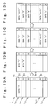
- the data 1 to be firstly stored as the data of the logical address X is written to the data region 7', the following writing process is carried out. At first, the data 1 is written to the memory region 71 1 without any condition. After the data 1 is written to the memory region 71 1 , the flag 72 1 is set to the state "1", and the flags 72 2 to 72 n are remained set to "0". Fig. 15A shows the state of the data region 7' after the completion of the process for writing the data 1.
- the address conversion program 12 refers to the flags 72 1 to 72 n , and determines which of the flags 72 1 to 72 n is "1". If the flag 72 k of the flags 72 1 to 72 n is determined to be "1" (k is an integer between 1 and n), the memory region 71 k+1 of the memory regions 71 1 to 71 n is selected as a destination to which the data after the update is written. However, if the flag 72 n is "1", the memory region 71 1 is selected as the destination to which the data after the update is written.
- the data of the logical address X after the update is written to the selected memory region 71 k+1 .
- the flag 72 n is at "1”
- the data of the logical address X after the update is written to the selected memory region 71 1 .
- the flag 71 k is updated from “1” to “0”, and the flag 71 k+1 is updated from “0” to “1". However, if the flag 72 n is “1", the flag 71 1 is updated from "0" to "1".
- the data 1 to be firstly stored as the data of the logical address X is written to the memory region 71 1 as shown in Fig. 15A.
- the flag 72 1 is set to "1”
- the flags 72 2 to 72 n are set to "0".
- the flags 72 1 to 72 n are referred. If the fact that the flag 72 1 is to "1" and the flags 72 2 to 72 n are "0" is detected, the memory region 71 2 of the memory regions 71 1 to 71 n is selected as the destination to which the data is written. The data 2 is written to the memory region 71 2 selected as the destination to which the data is written. Next, the flag 72 1 is updated to "0", and the flag 72 2 is updated to "1". The process for updating the data of the logical address X from the data 1 to the data 2 is ended as mentioned above.
- Fig. 15B shows the states of the data region 7' and the flags 72 1 to 72 n when the updating process is ended.
- the data of the logical address X is sequentially updated from the data 2 to the data 3, ..., and the data n
- the data 3, the data 4, ..., and the data n after the update are written to the memory region 71 3 , the memory region 71 4 , ..., the memory region 71 n , respectively.
- the flags of "1" of the flags 72 1 to 72 n are changed sequentially to the flag 72 3 , the flag 72 4 , ..., the flag 72 n .
- the data n is written to the memory region 71 n , as shown in Fig. 15C, and the flag 72 n of the flags 72 1 to 72 n is set to "1", and the other flags 72 1 to 72 n-1 are set to "0".
- the flags 72 1 to 72 n are referred, and the memory region 71 1 of the memory regions 71 1 to 71 n is selected as the destination to which the data is written.
- the data (n+1) is written to the memory region 71 1 selected as the destination to which the data is written.
- the flag 72 1 is updated to "1”
- the flag 72 n is updated to "0".
- the updating process for updating the data of the logical address X from the data n to the data (n+1) is ended as mentioned above.
- Fig. 15D shows the states of the data region 7' and the flags 72 1 to 72 n when the updating process is ended.
- the address conversion program 12 firstly refers to the flags 72 1 to 72 n , and determines which of the flags 72 1 to 72 n is "1". At this time, if the flag 72 k of the flags 72 1 to 72 n is determined to be "1", the data stored in the memory region 71 k of the memory regions 71 1 to 71 n is read out as the data of the logical address X. The operation for reading out the data from the data region 7' is ended as mentioned above.
- the programs for executing the above-mentioned operations is written in the main program 11 and the address conversion program 12 in this embodiment.
- the CPU 2 executes the above-mentioned operations in accordance with the main program 11 and the address conversion program 12.
- the data region 7 is reserved for the data, similarly to the semiconductor device in the first or second embodiments.
- the reserved data region 7 is comprised of the n memory regions 71 1 to 71 n (n is a natural number of 2 or more).
- n is a natural number of 2 or more.
- one of the memory regions 71 1 to 71 n is circularly selected as the destination to which the data is written.
- the data is written to the selected memory region.
- the permissive number of times of rewrite of the data is fictionally greater than the physically permissive number of times of rewrite of the non-volatile memory 4.
- the present invention provides the technique for fictionally extending the lifetime of the non-volatile memory in which the permissive number of times of rewrite is limited.
- the present invention provides the technique for simply determining a memory region to be used for the rewrite and performing the rotation on the memory regions, and thereby fictionally extending the lifetime of the non-volatile memory in which the permissive number of times of rewrite is limited.
- the present invention provides the technique for reducing the risk that the data stored in the non-volatile memory is damaged if the power supply to the non-volatile memory is interrupted during the access to the non-volatile memory.
- the present invention provides the technique for detecting the occurrence f the interruption of the power supply to the non-volatile memory if the power supply to the non-volatile memory is interrupted.
Landscapes
- Techniques For Improving Reliability Of Storages (AREA)
- Read Only Memory (AREA)
Abstract
Description
Condition: The
Claims (22)
- A semiconductor device comprising:a non-volatile memory (4); anda control unit (1, 2, 3) which reserves n memory regions (n is an integer equal to or more than 2) (711 to 71n) for n of data as first to n-th memory regions in said non-volatile memory and writes the data in said first memory region, when the data is written in said non-volatile memory, and each time the data is updated, sequentially and circularly writes the updated data as the latest data in said n memory regions.
- The semiconductor device according to claim 1, wherein said control unit reserves a pointer region (81) in said non-volatile memory to indicate an i-th one (i is an integer between 1 and n) of said first to n-th memory regions in which the latest data is written.
- The semiconductor device according to claim 2, wherein said control unit refers to said pointer region to read out the latest data from said i-th memory region.
- The semiconductor device according to claim 2 or 3, wherein when the latest data should be further updated, said control unit refers to said pointer region to read out the latest data from said i-th memory region, writes the updated data as the latest data in an (i+1)-th memory region if 1 ≦ i ≦ n-1, and in said first memory region if i = n, and updates said pointer region to indicate said (i+1)-th memory region or said first memory region.
- The semiconductor device according to any of claims 2 to 4, wherein said pointer region comprises (n-1) bit regions (811 to 81n-1) for said n memory regions, and an (j-1)-th bit region (j is an integer between 2 and n) of said (n-1) bit regions indicates said j-th memory region in which the latest data has been written.
- The semiconductor device according to claim 5, wherein said control unit changes a value of said (j-1)-th bit region from a first value to a second value when the latest data is written in said j-th memory region.
- The semiconductor device according to claim 6, wherein said control unit resets values of said (n-1) bit regions to the first value when the latest data is written in said first memory region.
- The semiconductor device according to any of claims 2 to 4, wherein said pointer region comprises n bit regions (721 to 72n) corresponding to said n memory regions, and an i-th bit region of said n bit regions indicates said i-th memory region in which the latest data has been written.
- The semiconductor device according to claim 8, wherein when the latest data is read out from an (i-1)-th memory region, updated and written in said i-th memory region, said control unit changes a value of said i-th bit region from a first value to a second value and changes a value of said (i-1)-th bit region from the second value to the first value.
- The semiconductor device according to any of claims 2 to 8, wherein said control unit reserves a power failure check region (82) in said non-volatile memory, andsaid power failure check region indicates whether power failure has occurred before the latest data is written in said i-th memory region.
- The semiconductor device according to claim 10, wherein when the latest data written in said i-th memory region should be further updated, said control unit refers to said pointer region and said power failure check region to determine an (i-1)-th memory region if said power failure check region indicates that the power failure has occurred when the latest data is written in said i-th memory region and said i-th memory region if said power failure check region indicates no power failure when the latest data is written in said i-th memory region, reads out the latest data from said determined memory region, and writes the updated data as the latest data in said memory region next to said determined memory region.
- The semiconductor device according to any of claims 1 to 11, wherein said control unit determines said n based on information supplied to said control unit.
- An IC card using the semiconductor device according to any of claims 1 to 12.
- A method of writing and updating data in a non-volatile memory, comprising the steps of:(a) reserving n memory regions (n is an integer equal to or more than 2) for n of data as first to n-th memory regions in a non-volatile memory, when the data is written in said non-volatile memory;(b) reserving a pointer region in said non-volatile memory, said pointer region indicating that the latest data is written an i-th one (i is an integer between 1 and n) of said first to n-th memory regions;(c) writing the data in said first memory region as the latest data;(d) sequentially and circularly writing the latest data in said n memory regions while said i increments by one each time the latest data is updated and the updated data is written as the latest data; and(e) updating said pointer region to indicate that the latest data has been written in said i-th memory region, when the latest data has been written in said i-th memory region.
- The method according to claim 14, wherein said (d) sequentially and circularly writing step comprises the step of:(f) referring to said pointer region to determine said i-th memory region, when said latest data is updated;(g) reading out the latest data from said i-th memory region; and(h) writing the updated data as the latest data in an (i+1)-th memory region.
- The method according to claim 15, wherein said (h) writing step comprises the steps of:writing the latest data in said (i+1)-th memory region if 1 ≦ i ≦ n-1; andwriting the latest data in said first memory region if i = n.
- The method according to any of claims 14 to 16, wherein said pointer region comprises (n-1) bit regions for said n memory regions, andsaid (e) updating step comprises the step of:changing a value of said (j-1)-th bit region from a first value to a second value when the latest data is written in said j-th memory region.
- The method according to claim 17, wherein said (e) updating step further comprises the step of:resetting values of said (n-1) bit regions to the first value when the latest data is written in said first memory region.
- The method according to any of claims 14 to 16, wherein said pointer region comprises n bit regions corresponding to said n memory regions, andsaid (e) updating step comprises the step of:when the latest data is read out from an (i-1)-th memory region, updated and written in said i-th memory region, changing a value of said i-th bit region from a first value to a second value and changes a value of said (i-1)-th bit region from the second value to the first value.
- The method according to any of claims 14 to 19, further comprising the step of:(i) reserving a power failure check region in said non-volatile memory, andwherein said (d) sequentially and circularly writing step further comprises the steps of:when the latest data written in said i-th memory region should be further updated, referring to said pointer region and said power failure check region to determine an (i-1)-th memory region if said power failure check region indicates that the power failure has occurred when the latest data is written in said i-th memory region and said i-th memory region if said power failure check region indicates no power failure when the latest data is written in said i-th memory region;reading out the latest data from said determined memory region; andwriting the updated data as the latest data in said memory region next to said determined memory region.
- The method according to any of claims 14 to 20, wherein said (a) reserving step comprises the step of:determining said n based on given information.
- A program for executing said method according to any of claims 14 to 21.
Applications Claiming Priority (2)
| Application Number | Priority Date | Filing Date | Title |
|---|---|---|---|
| JP2001073170A JP2002278850A (en) | 2001-03-14 | 2001-03-14 | Semiconductor device |
| JP2001073170 | 2001-03-14 |
Publications (2)
| Publication Number | Publication Date |
|---|---|
| EP1241677A1 true EP1241677A1 (en) | 2002-09-18 |
| EP1241677B1 EP1241677B1 (en) | 2006-06-07 |
Family
ID=18930635
Family Applications (1)
| Application Number | Title | Priority Date | Filing Date |
|---|---|---|---|
| EP20020005757 Expired - Lifetime EP1241677B1 (en) | 2001-03-14 | 2002-03-13 | Semiconductor device using non-volatile memory in which data is written circularly |
Country Status (3)
| Country | Link |
|---|---|
| EP (1) | EP1241677B1 (en) |
| JP (1) | JP2002278850A (en) |
| DE (1) | DE60211987T2 (en) |
Cited By (2)
| Publication number | Priority date | Publication date | Assignee | Title |
|---|---|---|---|---|
| WO2004027615A3 (en) * | 2002-09-20 | 2004-07-01 | Sharp Kk | Method of and apparatus for detecting an error in writing to persistent memory |
| EP2383746A1 (en) * | 2010-04-30 | 2011-11-02 | Proton World International N.V. | Method for writing and reading in an atomicity memory |
Families Citing this family (9)
| Publication number | Priority date | Publication date | Assignee | Title |
|---|---|---|---|---|
| KR100490603B1 (en) * | 2002-12-06 | 2005-05-27 | (주) 라모스테크놀러지 | Control method and apparatus for operations of flash memory system |
| NO324607B1 (en) * | 2003-11-24 | 2007-11-26 | Thin Film Electronics Asa | Method of operating a data storage device using passive matrix addressing |
| JP4586469B2 (en) * | 2004-09-15 | 2010-11-24 | ソニー株式会社 | MEMORY CONTROL DEVICE, MEMORY CONTROL METHOD, PROGRAM |
| JP2006085596A (en) * | 2004-09-17 | 2006-03-30 | Mitsubishi Electric Corp | Information recording / reading device |
| JP2006107363A (en) * | 2004-10-08 | 2006-04-20 | Toshiba Corp | Portable electronic device and memory access method used for portable electronic device |
| JP4529765B2 (en) * | 2005-03-31 | 2010-08-25 | コニカミノルタビジネステクノロジーズ株式会社 | Image forming apparatus |
| JP2008191855A (en) * | 2007-02-02 | 2008-08-21 | Sony Corp | Semiconductor memory device and memory control method |
| KR20100013485A (en) * | 2008-07-31 | 2010-02-10 | 삼성전자주식회사 | Memory device and method of wear leveling |
| JP2011198409A (en) * | 2010-03-19 | 2011-10-06 | Toshiba Information Systems (Japan) Corp | Nonvolatile memory |
Citations (5)
| Publication number | Priority date | Publication date | Assignee | Title |
|---|---|---|---|---|
| US4780855A (en) * | 1984-06-21 | 1988-10-25 | Nec Corporation | System for controlling a nonvolatile memory having a data portion and a corresponding indicator portion |
| JPH0421999A (en) * | 1990-05-15 | 1992-01-24 | Mitsubishi Electric Corp | Divided memory write system |
| FR2665791A1 (en) * | 1990-08-13 | 1992-02-14 | Mazingue Didier | Method of updating a EEPROM memory |
| FR2712412A1 (en) * | 1993-11-12 | 1995-05-19 | Peugeot | Safeguarding data in EEPROM microprocessor circuit in motor vehicle |
| FR2730833A1 (en) * | 1995-02-16 | 1996-08-23 | Gemplus Card Int | SECURE UPDATE OF EEPROM MEMORY |
-
2001
- 2001-03-14 JP JP2001073170A patent/JP2002278850A/en not_active Withdrawn
-
2002
- 2002-03-13 EP EP20020005757 patent/EP1241677B1/en not_active Expired - Lifetime
- 2002-03-13 DE DE2002611987 patent/DE60211987T2/en not_active Expired - Fee Related
Patent Citations (5)
| Publication number | Priority date | Publication date | Assignee | Title |
|---|---|---|---|---|
| US4780855A (en) * | 1984-06-21 | 1988-10-25 | Nec Corporation | System for controlling a nonvolatile memory having a data portion and a corresponding indicator portion |
| JPH0421999A (en) * | 1990-05-15 | 1992-01-24 | Mitsubishi Electric Corp | Divided memory write system |
| FR2665791A1 (en) * | 1990-08-13 | 1992-02-14 | Mazingue Didier | Method of updating a EEPROM memory |
| FR2712412A1 (en) * | 1993-11-12 | 1995-05-19 | Peugeot | Safeguarding data in EEPROM microprocessor circuit in motor vehicle |
| FR2730833A1 (en) * | 1995-02-16 | 1996-08-23 | Gemplus Card Int | SECURE UPDATE OF EEPROM MEMORY |
Non-Patent Citations (1)
| Title |
|---|
| PATENT ABSTRACTS OF JAPAN vol. 016, no. 182 (P - 1346) 30 April 1992 (1992-04-30) * |
Cited By (5)
| Publication number | Priority date | Publication date | Assignee | Title |
|---|---|---|---|---|
| WO2004027615A3 (en) * | 2002-09-20 | 2004-07-01 | Sharp Kk | Method of and apparatus for detecting an error in writing to persistent memory |
| US7539905B2 (en) | 2002-09-20 | 2009-05-26 | Sharp Kabushiki Kaisha | Method of and apparatus for detecting an error in writing to persistent memory |
| EP2383746A1 (en) * | 2010-04-30 | 2011-11-02 | Proton World International N.V. | Method for writing and reading in an atomicity memory |
| FR2959586A1 (en) * | 2010-04-30 | 2011-11-04 | Proton World Int Nv | METHOD OF WRITING AND READING IN AN ATOMICITY MEMORY |
| US9959930B2 (en) | 2010-04-30 | 2018-05-01 | Proton World International N.V. | Method for writing into and reading from an atomicity memory using marking pattern |
Also Published As
| Publication number | Publication date |
|---|---|
| EP1241677B1 (en) | 2006-06-07 |
| DE60211987D1 (en) | 2006-07-20 |
| DE60211987T2 (en) | 2007-02-01 |
| JP2002278850A (en) | 2002-09-27 |
Similar Documents
| Publication | Publication Date | Title |
|---|---|---|
| US6687784B2 (en) | Controller for controlling nonvolatile memory unit | |
| JP3215237B2 (en) | Storage device and method for writing / erasing storage device | |
| US7543137B2 (en) | Information processing device and information processing method | |
| US7061812B2 (en) | Memory card | |
| US6154808A (en) | Method and apparatus for controlling data erase operations of a non-volatile memory device | |
| US6098077A (en) | Data management apparatus, data management method, and recording medium | |
| US7070113B2 (en) | Nonvolatile memory card | |
| US6170066B1 (en) | Power-off recovery management for sector based flash media managers | |
| EP0544252A2 (en) | Data management system for programming-limited type semiconductor memory and IC memory card having the data management system | |
| US6865658B2 (en) | Nonvolatile data management system using data segments and link information | |
| US6745278B2 (en) | Computer capable of rewriting an area of a non-volatile memory with a boot program during self mode operation of the computer | |
| EP1241677B1 (en) | Semiconductor device using non-volatile memory in which data is written circularly | |
| US6883060B1 (en) | Microcomputer provided with flash memory and method of storing program into flash memory | |
| US20040139310A1 (en) | Information processing apparatus, memory management apparatus, memory management method, and information processing method | |
| US20020002652A1 (en) | Method of rewriting program in flash microcomputer | |
| US6839798B1 (en) | Flash memory capable of storing frequently rewritten data | |
| KR20010109336A (en) | Method and apparatus to permit adjustable code/data boundary in a nonvolatile memory | |
| US20080250188A1 (en) | Memory Controller, Nonvolatile Storage, Nonvolatile Storage System, and Memory Control Method | |
| JP4999325B2 (en) | Flash memory | |
| JP2000222292A (en) | Data managing method utilizing flash memory | |
| JP4158526B2 (en) | Memory card and data writing method to memory | |
| US6646917B1 (en) | Storage device managing nonvolatile memory by converting logical address to physical address of nonvolatile memory | |
| KR100654344B1 (en) | Memory device and its error recovery method using flash memory | |
| JP2001312891A (en) | Semiconductor memory device | |
| US7346730B2 (en) | Mobile electronic device |
Legal Events
| Date | Code | Title | Description |
|---|---|---|---|
| PUAI | Public reference made under article 153(3) epc to a published international application that has entered the european phase |
Free format text: ORIGINAL CODE: 0009012 |
|
| AK | Designated contracting states |
Kind code of ref document: A1 Designated state(s): AT BE CH CY DE DK ES FI FR GB GR IE IT LI LU MC NL PT SE TR |
|
| AX | Request for extension of the european patent |
Free format text: AL;LT;LV;MK;RO;SI |
|
| 17P | Request for examination filed |
Effective date: 20020905 |
|
| 17Q | First examination report despatched |
Effective date: 20021203 |
|
| RAP1 | Party data changed (applicant data changed or rights of an application transferred) |
Owner name: NEC ELECTRONICS CORPORATION |
|
| AKX | Designation fees paid |
Designated state(s): DE FR |
|
| GRAP | Despatch of communication of intention to grant a patent |
Free format text: ORIGINAL CODE: EPIDOSNIGR1 |
|
| GRAS | Grant fee paid |
Free format text: ORIGINAL CODE: EPIDOSNIGR3 |
|
| GRAA | (expected) grant |
Free format text: ORIGINAL CODE: 0009210 |
|
| AK | Designated contracting states |
Kind code of ref document: B1 Designated state(s): DE FR |
|
| REF | Corresponds to: |
Ref document number: 60211987 Country of ref document: DE Date of ref document: 20060720 Kind code of ref document: P |
|
| ET | Fr: translation filed | ||
| PLBE | No opposition filed within time limit |
Free format text: ORIGINAL CODE: 0009261 |
|
| STAA | Information on the status of an ep patent application or granted ep patent |
Free format text: STATUS: NO OPPOSITION FILED WITHIN TIME LIMIT |
|
| 26N | No opposition filed |
Effective date: 20070308 |
|
| PGFP | Annual fee paid to national office [announced via postgrant information from national office to epo] |
Ref country code: DE Payment date: 20070523 Year of fee payment: 6 |
|
| PGFP | Annual fee paid to national office [announced via postgrant information from national office to epo] |
Ref country code: FR Payment date: 20070328 Year of fee payment: 6 |
|
| REG | Reference to a national code |
Ref country code: FR Ref legal event code: ST Effective date: 20081125 |
|
| PG25 | Lapsed in a contracting state [announced via postgrant information from national office to epo] |
Ref country code: DE Free format text: LAPSE BECAUSE OF NON-PAYMENT OF DUE FEES Effective date: 20081001 |
|
| PG25 | Lapsed in a contracting state [announced via postgrant information from national office to epo] |
Ref country code: FR Free format text: LAPSE BECAUSE OF NON-PAYMENT OF DUE FEES Effective date: 20080331 |