EP1239714A2 - Terminal holding and heat dissipation structure - Google Patents
Terminal holding and heat dissipation structure Download PDFInfo
- Publication number
- EP1239714A2 EP1239714A2 EP02251588A EP02251588A EP1239714A2 EP 1239714 A2 EP1239714 A2 EP 1239714A2 EP 02251588 A EP02251588 A EP 02251588A EP 02251588 A EP02251588 A EP 02251588A EP 1239714 A2 EP1239714 A2 EP 1239714A2
- Authority
- EP
- European Patent Office
- Prior art keywords
- terminal
- soldering
- plate
- substrate
- portions
- Prior art date
- Legal status (The legal status is an assumption and is not a legal conclusion. Google has not performed a legal analysis and makes no representation as to the accuracy of the status listed.)
- Granted
Links
Images


Classifications
-
- B—PERFORMING OPERATIONS; TRANSPORTING
- B60—VEHICLES IN GENERAL
- B60R—VEHICLES, VEHICLE FITTINGS, OR VEHICLE PARTS, NOT OTHERWISE PROVIDED FOR
- B60R16/00—Electric or fluid circuits specially adapted for vehicles and not otherwise provided for; Arrangement of elements of electric or fluid circuits specially adapted for vehicles and not otherwise provided for
- B60R16/02—Electric or fluid circuits specially adapted for vehicles and not otherwise provided for; Arrangement of elements of electric or fluid circuits specially adapted for vehicles and not otherwise provided for electric constitutive elements
- B60R16/023—Electric or fluid circuits specially adapted for vehicles and not otherwise provided for; Arrangement of elements of electric or fluid circuits specially adapted for vehicles and not otherwise provided for electric constitutive elements for transmission of signals between vehicle parts or subsystems
- B60R16/0239—Electronic boxes
-
- H—ELECTRICITY
- H05—ELECTRIC TECHNIQUES NOT OTHERWISE PROVIDED FOR
- H05K—PRINTED CIRCUITS; CASINGS OR CONSTRUCTIONAL DETAILS OF ELECTRIC APPARATUS; MANUFACTURE OF ASSEMBLAGES OF ELECTRICAL COMPONENTS
- H05K3/00—Apparatus or processes for manufacturing printed circuits
- H05K3/30—Assembling printed circuits with electric components, e.g. with resistor
- H05K3/301—Assembling printed circuits with electric components, e.g. with resistor by means of a mounting structure
-
- H—ELECTRICITY
- H05—ELECTRIC TECHNIQUES NOT OTHERWISE PROVIDED FOR
- H05K—PRINTED CIRCUITS; CASINGS OR CONSTRUCTIONAL DETAILS OF ELECTRIC APPARATUS; MANUFACTURE OF ASSEMBLAGES OF ELECTRICAL COMPONENTS
- H05K3/00—Apparatus or processes for manufacturing printed circuits
- H05K3/30—Assembling printed circuits with electric components, e.g. with resistor
- H05K3/306—Lead-in-hole components, e.g. affixing or retention before soldering, spacing means
Definitions
- the present invention relates to a terminal structure of a straight terminal such as a wide terminal for conducting a large current to be attached to a printed circuit board for an electronic control unit (ECU) or the like by soldering.
- the invention relates to a holding structure and a heat dissipating structure thereof.
- a terminal holding structure of this type one disclosed in JP-A-2000-68622 shown in Figs. 20A and 20B is known.
- a pair of upper and lower projecting portions 2 and 3 jutting out laterally with an interval corresponding to the thickness of a printed circuit board 5 therebetween are provided at a proximal portion of a plate-like straight terminal 1, as shown in Figs. 20A and 20B.
- the lower projecting portion 3 jutting out from both lateral sides of the proximal portion of the terminal 1 is inserted through a pair of semicircular slits 6a formed in an inner peripheral surface of the attaching hole 6 at positions opposing each other in the diametrical direction of the attaching hole 6, and the pair of projecting portions 2 and 3 are engaged with peripheral edge portions of the attaching hole 6 by rotating the terminal 1 by a predetermined angle.
- soldered portion solder fillet
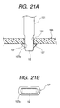
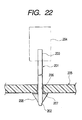
- FIG. 21A Another terminal structures of related art are shown in Figs. 21A, 21B and Fig. 22.
- a soldering portion 102 at a lower end of a plate-like wide terminal 101 for conducting a large current is inserted into a connecting hole 106 formed in a printed circuit board 105, and the soldering portion 102 of the terminal 101 is fixed by soldering to a land portion 107 formed around the connecting hole 106 on the lower surface of the printed circuit board 105.
- the land portion 107 is formed in a substantially annular elliptical shape having an elliptical elongated hole 107a in its center.
- a soldered portion (solder fillet) is denoted by reference numeral 108 in Fig. 21A.
- a soldering portion 202 at a lower end of a straight terminal 201 is inserted into a connecting hole 206 formed in a printed circuit board 205, and the soldering portion 202 of the terminal 201 is fixed by soldering to a land portion 207 formed around the connecting hole 206 on the lower surface of the printed circuit board 205.
- a heat generating component 204 such as a fuse or a relay is detachably connected to an upper end 203 of the terminal 201.
- a soldered portion (solder fillet) is denoted by reference numeral 208 in Fig. 22.
- the holding structure of the terminal 101 since the land portion 107 which is formed on the lower surface of the printed circuit board 105 has in its center the elliptical elongated hole 107a, the durability of the land portion 107 has been inferior and liable to be damaged. Hence, the fabrication cost of the printed circuit board 105 has been high to improve the quality.
- the invention has been devised to overcome the above-described problems, and its object is to provide a terminal structure which makes it possible to alleviate stresses including the mechanical stress and the thermal stress applied to the soldered portion, thereby making it possible to reliably prevent the occurrence of the solder crack.
- a holding structure of a terminal and a substrate wherein a soldering portion of the terminal is inserted into a connecting hole of the substrate, and a land portion provided on the substrate and the soldering portion of the terminal are held by soldering with the terminal which is set upright
- the holding structure comprising: a terminal plate for guiding the soldering portion into the connecting hole to a position opposing the substrate, forming a predetermined clearance; a positioning hole for holding an intermediate portion of the terminal provided in the terminal plate; and a retaining portion retained in the positioning hole of the terminal plate is provided in the intermediate portion of the terminal.
- the retaining portion provided in the intermediate portion of the terminal is retained in the positioning hole of the terminal plate which is disposed at a position opposing the substrate and spaced apart therefrom with a predetermined clearance, when an electric component is attached to or detached from the terminal, a mechanical stress applied to a soldered portion between the soldering portion of the terminal and a land portion on the substrate is alleviated.
- the retaining portion of the terminal which is retained in the positioning hole of the terminal plate is located away from the soldered portion, a thermal stress applied to the soldered portion is alleviated.
- the retaining portion of the terminal and the land portion on the substrate are located away from each other, the land portion is not damaged by the retaining portion of the terminal. For these reasons, the occurrence of the solder crack in the soldered portion is reliably prevented.
- the terminal holding structure according to (1) wherein the positioning hole of the terminal plate is formed on a terminal press-fitting portion projecting upwardly from an upper surface of the terminal plate.
- the positioning hole of the terminal plate is provided in the terminal press-fitting portion projecting upwardly from the upper surface of the terminal plate, a sufficient distance is secured between the retaining portion of the terminal and the soldered portion, thereby alleviating stresses such as the mechanical stress and the thermal stress applied to the soldered portion.
- the environmental heat in the surroundings and the heat generated by such as the self heating of a heat generating component connected to the terminal are dissipated from the retaining portion of the terminal to the terminal plate side, thereby improving the heat dissipating effect.
- a holding structure of a terminal and a substrate comprising: a plurality of soldering portions formed by dividing a soldering proximal portion of the terminal into small portions; wherein the soldering portions are held on a land portion of the substrate by soldering.
- a heat dissipating structure for a terminal wherein one end of the terminal is connectable to a heat generating component and another end of the terminal is soldered in an upright state to a substrate
- heat dissipating structure comprising: a wide flat portion formed by being bent at an intermediate portion of the terminal; a heat insulating plate disposed at a position opposing the substrate with a predetermined clearance; wherein the flat portion of the terminal is made capable of freely abutting against a terminal pressing portion provided on the heat insulating plate.
- the heat dissipating structure for a terminal according to (6) wherein a resin plate cover for covering the heat insulating plate is provided in such a manner as to be spaced apart from the heat insulating plate with a predetermined clearance, and the flat portion of the terminal is capable of being freely clamped by the terminal pressing portion of the heat insulating plate and a terminal pressing portion provided on the plate cover.
- the dynamic stress applied to the soldered portion is alleviated. For these reasons, stresses including the thermal stress and the dynamic stress applied to the soldered portion are alleviated, thereby reliably preventing the occurrence of the solder crack in the soldered portion.
- Fig. 1 is an exploded front elevational view illustrating an electric junction box of an electronic control unit-integrated type.
- Fig. 2 is a front elevational view of the electric junction box.
- Fig. 3 is a plan view of the electric junction box.
- Fig. 4 is a plan view of an electronic control unit incorporated in the electric junction box.
- Fig. 5 is a front elevational view of the electronic control unit.
- Fig. 6 is a cross-sectional view taken along line D - D in Fig. 5.
- Fig. 7 is a cross-sectional view taken along line A - A in Fig. 4.
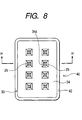
- Fig. 8 is an enlarged plan view of a portion E in Fig. 6.
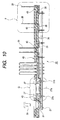
- Fig. 9 is a cross-sectional view taken along line H - H in Fig. 8.
- Fig. 10 is a cross-sectional view taken along line B - B in Fig. 4.
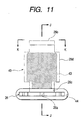
- Fig. 11 is an enlarged plan view of a portion F in Fig. 6.
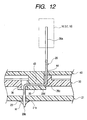
- Fig. 12 is a cross-sectional view taken along line J - J in Fig. 11.
- Fig. 13 is a cross-sectional view taken along line K - K in Fig. 11.
- Fig. 14 is an explanatory diagram of a land portion used in the electronic control unit.
- Fig. 15 is a perspective view illustrating the relationship between the land portion and a terminal.
- Fig. 16 is an enlarged view of a portion G in Fig. 6.
- Fig. 17 is a cross-sectional view taken along line P - P in Fig. 16.
- Fig. 18 is a cross-sectional view taken along line C - C in Fig. 4.
- Fig. 19 is a right-hand side elevational view of the electronic control unit.
- an electric junction box 10 of an electronic control unit-integrated type is mainly comprised of a box-shaped upper casing 11 made of a synthetic resin; a box-shaped main cover 12 made of a synthetic resin and adapted to be fitted to the upper casing 11 engageably and disengageably; a bus bar layer 13 disposed on an upper surface side of the main cover 12; and an electronic control unit (ECU) 20 incorporated between the upper casing 11 and the main cover 12 on the lower side of the bus bar layer 13.
- this electric junction box 10 is used for the main purpose of distributing the power source of an automobile, for instance, and the electronic control unit 20 controls the turning on and off of an engine, lights, wipers, and the like of the automobile, for instance.
- the bus bar layer 13 is arranged such that a plurality of bus bars 15 are routed on an insulating board 14, and their one end sides are formed by being bent upwardly as insulation displacing portions 15a formed in the shape of slit blades and the like.
- These insulation displacing portions 15a and the like of the bus bars 15 respectively project so as to extend to relay fitting portions 12a and fuse fitting portions 12b which are integrally formed projectingly on the upper surface side of the main cover 12 shown in Fig. 3.
- Plug-in relays 16 serving as electronic components are fitted in the relay fitting portions 12a, and fuses 17 serving as electronic components are fitted in the fuse fitting portions 12b.
- the electronic control unit 20 is comprised of a rectangular plate-shaped main board (substrate) 21 which is made of a synthetic resin and on which straight terminals 25 and crank-shaped terminals 26, as well as resistors 27, relays 28, and the like serving as electronic components, are respectively mounted; a substantially plate-shaped terminal plate (heat insulating plate) 30 which is made of a synthetic resin and to a lower surface side of which the main board 21 is fixed by screws 39 or the like so as to oppose the terminal plate 30 and to be spaced apart therefrom with a predetermined clearance with a plurality of hollow cylindrical boss portions 31 interposed therebetween; a plate-shaped plate cover 40 which is made of a synthetic resin and is disposed so as to be located above and oppose a portion of the terminal plate 30 (excluding the area of a frame-shaped holding plate 33) in such a manner as to be spaced apart therefrom with a predetermined clearance in a state in which a plurality of projecting portions 41 such as hook portions
- soldering portions 25a at the lower ends of the straight, rod-shaped terminals 25 are adapted to be respectively guided into connecting holes 21a of the main board 21 by the terminal plate 30.
- the positions of the connecting holes 21a in the main board 21 and positioning holes 34a in the terminal plate 30 for holding intermediate portions 25b of the terminals 25 are aligned, and soldering portions 25a of the terminals 25 are guided and inserted into the connecting holes 21a of the main board 21 at a position opposing the main board 21 and spaced apart therefrom with a predetermined clearance.
- soldering portions 25a of the terminals 25 inserted into the connecting holes 21a of the main board 21 are adapted to be soldered to land portions 22 formed on the lower surface of the main board 21 with the terminals 25 set vertically upright, and are held by the main board 21.
- soldered portions solder fillets
- each terminal 25 has a projecting portion (retaining portion) 25c which is formed integrally in such a manner as to project annularly and which is retained in the positioning hole 34a of the terminal plate 30.
- the positioning holes 34a of the terminal plate 30 are provided in two rows in the center of a terminal press-fitting portion 34 which projects in a block shape upwardly from the upper surface of the terminal plate 30.
- This terminal press-fitting portion 34 projects upwardly of an opening 42 in the plate cover 40, and an upper end 25d of the terminal 25 exposed from the terminal press-fitting portion 34 projects up to a connector fitting portion 12c of the main cover 12.
- An external connector 18 serving as an electric component is adapted to be engaged with this upper end 25d of the terminal 25.
- each terminal 25 is retained by being press fitted to a predetermined position in the positioning hole 34a of the terminal plate 30, and this retained state is such that the projecting portion 25c of the terminal 25 is sufficiently prevented from becoming dislocated by a mechanical stress caused by the attachment or detachment of the external connector 18.
- the terminals 26 for a large current which are cranked in the L-shape and are wide as a whole, have upper ends (one ends) formed as insulation displacing portions 26a in the shape of slit blades, and heat generating components such as the plug-in relays 16 or the fuses 17 and the external connectors 18 are connectable thereto.
- a pair of bifurcated soldering portions 26b at the lower end (the other end) of each terminal 26 are inserted into connecting holes 21b of the main board 21 with the terminals 26 set vertically upright, are soldered to land portions 23 formed on the lower surface of the main board 21, and are held by the main board 21.
- These soldered portions soldered portions (solder fillets) are denoted by reference character H.
- a wide flat portion 26d is formed in an intermediate portion 26c of the terminal 26 by being bent so as to be parallel with the main board 21.
- This flat portion 26d is capable of freely abutting against a terminal pressing portion 35 of the terminal plate 30, which is disposed at a position opposing the main board 21 and spaced apart therefrom with predetermined clearance.
- the wide flat portion 26d of the terminal 26 is capable of freely abutting against a terminal pressing portion 43 which is provided on the resin plate cover 40 covering the terminal plate 30 and spaced apart from the terminal plate 30 with a predetermined clearance. Namely, the wide flat portions 26d of the terminal 26 are respectively clamped by the terminal pressing portions 35 of the terminal plate 30 and the terminal pressing portions 43 of the plate cover 40.
- terminal inserting holes 36 and 44 are respectively formed in the vicinities of the terminal pressing portions 35 and 43 of the terminal plate 30 and the plate cover 40.
- the insulation displacing portions 26a of the terminals 26 exposed from the terminal inserting holes 44 of the plate cover 40 project to the relay fitting portions 12a, the fuse fitting portions 12b, the connector fitting portions 12c, and the like.
- the terminal pressing portion 43 of the plate cover 40 is formed to be wide with the substantially same shape as that of the wide flat portion 26d of the terminal 26.
- the terminal pressing portion 35 of the terminal plate 30 is similarly formed to be wide.
- the lower end of the wide terminal 26 cranked in the L-shape is segmented by being bifurcated as the soldering portions 26b.
- the pair of connecting holes 21b are respectively formed in the main board 21 at positions opposing the pair of soldering portions 26b of the terminal 26.
- a pair of round terminal inserting holes 23a are respectively formed in the land portion 23 at positions opposing the pair of soldering portions 26b of the terminal 26.
- a pair of indented portions 23b are formed on both peripheral sides of a central portion of the land portion 23 located between the pair of terminal inserting holes 23a of the land portion 23.
- a component accommodating portion 37 for accommodating and holding a resistor (heat generating component) 27 is formed at a predetermined position on the terminal plate 30 in a recessed manner.
- each lead portion 27b and a land portion 24 formed on the lower surface side of the main board 21 are held in such a manner as to be capable of being freely fixed by soldering in a state in which the respective lead portions 27b of the resistor 27 are inserted in the inserting holes 37a and 21c of the recessed component accommodating portion 37 and the main board 21, and the component body 27a of the resistor 27 is spaced apart from a bottom surface 37b of the recessed component accommodating portion 37.
- the soldered portion (solder fillet) is denoted by reference character H.
- an opening 45 of the same shape as that of the component accommodating portion 37 is formed in the plate cover 40 at a position opposing the component accommodating portion 37.
- the main board 21, on which heat generating components such as the resistors 27 and the relays 28 are mounted by means of the frame-shaped holding plate 33 integrally formed projectingly on the right side of the terminal plate 30, and the control board 50, on which the control components 51 and 52 such as the microcomputer (CPU) are mounted, are held and laminated in such a manner as to be spaced apart a predetermined distance.
- a heat insulating plate 38 is integrally formed on upper ends of a pair of side wall portions 33a of the holding plate 33.
- An air layer S is formed between the heat insulating plate 38 and the control board 50 in a state in which a plurality of projecting portions 38a integrally formed projectingly on the upper surface of the heat insulating plate 38 are interposed therebetween.
- control board 50 is positioned by means of a plurality of hook portions 33b, which are integrally formed projectingly on the pair of side wall portions 33a of the holding plate 33 and the heat insulating plate 38, and are retained by a plurality of recessed portions 54 formed in the control board 50. Further, the air layer S between the heat insulating plate 38 and the control board 50 is constantly maintained at a fixed value with the projecting portions 38a of the heat insulating plate 38 interposed therebetween.
- the arrangement provided is such that, as shown in Fig. 9, the projecting portion 25c which is integrally formed projectingly on the intermediate portion 25b of each straight, rod-shaped terminal 25 is retained by being press fitted in the positioning hole 34a of the terminal plate 30 disposed at the position opposing the main board 21 and spaced apart therefrom with a predetermined clearance. Accordingly, when the external connector 18 is attached to or detached from the terminal 25, it is possible to alleviate the mechanical stress applied to the soldered portion H between the soldering portion 25a of the terminal 25 and the land portion 22 on the main board 21.
- the projecting portion 25c which serves as a point of fixation of the terminal 25 retained in the positioning hole 34a of the terminal plate 30, is disposed away from the soldered portion H, it is possible to alleviate the thermal stress applied to the soldered portion H. Furthermore, since the projecting portion 25c of the terminal 25 and the land portion 22 on the main board 21 are not located in close proximity to each other in the conventional manner, but are located away from each other, the land portion 22 on the main board 21 is not damaged by the projecting portion 25c of the terminal 25. For these reasons, it is possible to reliably prevent the occurrence of the solder cracks in the soldered portion H.
- the positioning holes 34a of the terminal plate 30, in which the projecting portions 25c of the terminals 25 are retained, are formed in the terminal press-fitting portion 34 projecting upwardly from the upper surface of the terminal plate 30, it is possible to secure a sufficient distance (clearance) from the projecting portion 25c of the respective terminal 25 to the soldered portion H, thereby making it possible to reliably alleviate stresses including the mechanical stress and the thermal stress applied to the soldered portion H.
- the environmental heat in the surroundings including the engine heat, as well as the heat generated by such as the self heating of heat generating components including the relays 28 connected to the terminals 26 in the vicinities of the terminals 25, can be reliably dissipated from the projecting portions 25c of the terminals 25 to the side of the synthetic resin terminal plate 30 serving as the heat insulating plate, thereby making it possible to further improve the heat dissipating effect.
- the arrangement provided is such that, as shown in Figs. 12 and 13, the soldering portion of the wide terminal 26 for large-current use is divided into small portions by being bifurcated as the soldering portions 26b.
- solder stress due to the heat heat generated by such as the self heating of a heat generating component including the relay 16 connected to the insulation displacing portion 26a of the terminal 26
- the soldered portion H between, on the one hand, the pair of soldering portions 26b of the terminal 26 and, on the other hand, the land portion 23 on the main board 21 can be dispersed and alleviated by the pair of soldering portions 26b of the terminal 26.
- the pair of connecting holes 21b are respectively formed in the main board 21 at positions opposing the pair of soldering portions 26b of the terminal 26, and the pair of round terminal inserting holes 23a are respectively formed in the land portion 23 at positions opposing the pair of soldering portions 26b of the terminal 26, a high-quality land portion 23 can be formed simply, thereby making it possible to lower the cost of the overall main board 21.
- the flat portion 26d of the terminal 26 is clamped between the terminal pressing portion 35 of the terminal plate 30 and the terminal pressing portion 43 of the plate cover 40, when the external connector 18 or the like is attached to or detached from the insulation displacing portion 26a of the terminal 26, it is possible to alleviate the dynamic stress applied to the soldered portion H between each of the pair of soldering portions 26b of the terminal 26 and the land portion 23 on the main board 21. For these reasons, it is possible to reliably prevent the occurrence of the solder crack in the soldered portion H.
- the arrangement provided is such that, as shown in Fig. 12, the wide flat portion 26d is formed by being bent at the intermediate portion 26c of the terminal 26, and the terminal plate 30 is disposed at a position opposing the main board 21 and spaced apart therefrom with a predetermined clearance, and the flat portion 26d of the terminal 26 is made capable of freely abutting against the terminal pressing portion 35 provided on the terminal plate 30.
- the environmental heat in the surroundings including the engine heat, which is transmitted to the soldered portion H between the soldering portion 26b of the terminal 26 and the land portion 23 on the main board 21, as well as the heat generated by such as the self heating of the relay 16 or the fuse 17 connected to the insulation displacing portion 26a of the terminal 26, can be dissipated to the terminal pressing portion 35 side of the terminal plate 30 through the flat portion 26d of the terminal 26, thereby making it possible to improve the heat dissipating effect.
- the flat portion 26d of the terminal 26 is made capable of being freely clamped by the terminal pressing portion 35 of the terminal plate 30 and the terminal pressing portion 43 of the plate cover 40 for covering the terminal plate 30, the heat which is caused by the self heating of the relay 15 or the fuse 17 connected to the insulation displacing portion 26a of the terminal 26, and which is transmitted to the soldered portion H, can be efficiently dissipated to the sides of the terminal pressing portions 35 and 43 of the terminal plate 30 serving as the synthetic resin heat insulating plate and the synthetic resin plate cover 40, respectively, through the wide flat portion 26d of the terminal 26, thereby making it possible to further improve the heat dissipating effect of the heat generating components such as the relays 16 and the fuses 17.
- the flat portion 26d of the terminal 26 is arranged to be freely clamped and fixed by the terminal pressing portion 35 of the terminal plate 30 and the terminal pressing portion 43 of the plate cover 40, when the relay 16, the fuse 17, or the like is attached to or detached from the insulation displacing portion 26a of the terminal 26, it is possible to reliably alleviate the dynamic stress applied to the soldered portion H between the soldering portion 26b of the terminal 26 and the land portion 23 on the main board 21.
- the retaining portion provided in the intermediate portion of the terminal is retained in the positioning hole of the terminal plate which is disposed at a position opposing the substrate and spaced apart therefrom with a predetermined clearance, when an electric component is attached to or detached from the terminal, it is possible to alleviate a mechanical stress applied to a soldered portion between the soldering portion of the terminal and a land portion on the substrate.
- the retaining portion of the terminal which is retained in the positioning hole of the terminal plate is located away from the soldered portion, it is possible to alleviate a thermal stress applied to the soldered portion.
- the retaining portion of the terminal and the land portion on the substrate are located away from each other, the land portion on the substrate is prevented from becoming damaged by the retaining portion of the terminal. For these reasons, the occurrence of solder cracks in the soldered portions can be reliably prevented.
- the positioning hole of the terminal plate is provided in the terminal press-fitting portion projecting upwardly from the upper surface of the terminal plate, it is possible to secure a sufficient distance between the retaining portion of the terminal and the soldered portion, thereby making it possible to alleviate stresses such as the mechanical stress and the thermal stress applied to the soldered portion.
- the environmental heat in the surroundings and the heat generated by such as the self heating of a heat generating component connected to the terminal can be dissipated from the retaining portion of the terminal to the terminal plate side, thereby making it possible to improve the heat dissipating effect.
- connecting holes are respectively formed in the substrate at positions opposing the plurality of soldering portions, and round terminal inserting holes are respectively formed in the land portion at positions opposing the plurality of soldering portions, a high-quality substrate can be fabricated at low cost.
- the indented portion is formed in a peripheral side of the central portion of the land portion between the terminal inserting holes, a satisfactory solder fillet can be formed by means of this indented portion, thereby making it possible to improve the durability of the soldered portion.
- the arrangement provided is such that a wide flat portion is formed by being bent at an intermediate portion of the terminal, that a heat insulating plate is disposed at a position opposing the substrate and spaced apart therefrom with a predetermined clearance, and that the flat portion of the terminal is made capable of freely abutting against a terminal pressing portion provided on the heat insulating plate.
- heat which is caused by the self heating of a heat generating component connected to one end side of the terminal, and which is transmitted to the soldered portion between the other end side of the terminal and the substrate, can be dissipated to the terminal pressing portion side of the heat insulating plate through the wide flat portion at the intermediate portion of the terminal, thereby making it possible to further improve the heat dissipating effect.
- the wide flat portion at the intermediate portion of the terminal abuts against the terminal pressing portion of the heat insulating plate and is located away from the soldered portion, it is possible to alleviate the thermal stress applied to the soldered portion. For these reasons, the occurrence of a solder crack in the soldered portion can be prevented.
- the flat portion of the terminal is capable of being freely clamped by the terminal pressing portion provided on the heat insulating plate and the terminal pressing portion provided on the plate cover for covering the heat insulating plate, the heat which is caused by the self heating of a heat generating component connected to one end side of the terminal, and which is transmitted to the soldered portion between the other end side of the terminal and the substrate, can be efficiently dissipated to the sides of the respective terminal pressing portions of the heat insulating plate and the plate cover, respectively, through the flat portion of the terminal, thereby making it possible to further improve the heat dissipating effect.
- the wide flat portion at the intermediate portion of the terminal is made capable of being freely clamped and fixed by the terminal pressing portion of the heat insulating plate and the terminal pressing portion of the plate cover, when the heat generating component is attached to or detached from one end side of the terminal, the dynamic stress applied to the soldered portion can be alleviated. For these reasons, stresses including the thermal stress and the dynamic stress applied to the soldered portion can be alleviated, thereby making it possible to reliably prevent the occurrence of the solder crack in the soldered portion.
Abstract
Description
- The present invention relates to a terminal structure of a straight terminal such as a wide terminal for conducting a large current to be attached to a printed circuit board for an electronic control unit (ECU) or the like by soldering. Particularly, the invention relates to a holding structure and a heat dissipating structure thereof.
- As a terminal holding structure of this type, one disclosed in JP-A-2000-68622 shown in Figs. 20A and 20B is known. In this holding structure, a pair of upper and lower projecting
portions circuit board 5 therebetween are provided at a proximal portion of a plate-likestraight terminal 1, as shown in Figs. 20A and 20B. - Further, when the
terminal 1 is inserted into an attachinghole 6 of the printedcircuit board 5, the lower projectingportion 3 jutting out from both lateral sides of the proximal portion of theterminal 1 is inserted through a pair ofsemicircular slits 6a formed in an inner peripheral surface of the attachinghole 6 at positions opposing each other in the diametrical direction of the attachinghole 6, and the pair of projectingportions hole 6 by rotating theterminal 1 by a predetermined angle. In the state in which the printedcircuit board 5 is clamped by the pair of projectingportions terminal 1, the proximal portion of theterminal 1 and aland portion 7 formed around the attachinghole 6 of the printedcircuit board 5 are soldered so as to mount theterminal 1 in a state of being set vertically upright on the printedcircuit board 5. This soldered portion (solder fillet) is denoted byreference numeral 8. - However, with the above-described conventional structure for holding the
terminal 1 on the printedcircuit board 5, since soldering is effected in such a manner as to completely cover the pair of projectingportions terminal 1 for clamping the printed circuit board 5 (i.e., the distance between each of the pair of projectingportions terminal 1 and the solderedportion 8 is very small), when an electric component such as an external connector is attached to or detached from theterminal 1, a large mechanical stress is directly applied to the solderedportion 8 from the vertical direction through the pair of projectingportions terminal 1. Hence, a solder crack has been liable to occur in the solderedportion 8. In addition, a large thermal stress is directly applied to the solderedportion 8 through the pair of projectingportions terminal 1 due to the environmental heat in the surroundings and the heat generated by such as the self heating of an electronic component including a fuse or a relay connected to theterminal 1. Hence, a solder crack has been liable to occur in the solderedportion 8. Furthermore, since the structure adopted is such that theland portion 7 on the printedcircuit board 5 is clamped by the pair of projectingportions terminal 1, theland portion 7 has been liable to be damaged by the pair of projectingportions terminal 1. - Another terminal structures of related art are shown in Figs. 21A, 21B and Fig. 22. In the holding structure shown as in Fig. 21A, a
soldering portion 102 at a lower end of a plate-likewide terminal 101 for conducting a large current is inserted into a connectinghole 106 formed in a printedcircuit board 105, and the solderingportion 102 of theterminal 101 is fixed by soldering to aland portion 107 formed around the connectinghole 106 on the lower surface of the printedcircuit board 105. As shown in Fig. 21B, theland portion 107 is formed in a substantially annular elliptical shape having an ellipticalelongated hole 107a in its center. A soldered portion (solder fillet) is denoted byreference numeral 108 in Fig. 21A. - In the terminal structure shown in Fig. 22, a
soldering portion 202 at a lower end of astraight terminal 201 is inserted into a connectinghole 206 formed in a printedcircuit board 205, and thesoldering portion 202 of theterminal 201 is fixed by soldering to aland portion 207 formed around the connectinghole 206 on the lower surface of the printedcircuit board 205. Aheat generating component 204 such as a fuse or a relay is detachably connected to anupper end 203 of theterminal 201. A soldered portion (solder fillet) is denoted byreference numeral 208 in Fig. 22. - However, with the above-described conventional structures for attaching the
terminals circuit boards - Further, in the holding structure of the
terminal 101, since theland portion 107 which is formed on the lower surface of the printedcircuit board 105 has in its center the ellipticalelongated hole 107a, the durability of theland portion 107 has been inferior and liable to be damaged. Hence, the fabrication cost of the printedcircuit board 105 has been high to improve the quality. - In the holding structure of the
terminal 201, when theheat generating component 204 is attached to or detached from theupper end 203 of theterminal 201, a large mechanical stress is directly applied from the vertical direction to the solderedportion 208 through thesoldering portion 202 of theterminal 201. Hence, a solder crack has been liable to occur in the solderedportion 208. - Accordingly, the invention has been devised to overcome the above-described problems, and its object is to provide a terminal structure which makes it possible to alleviate stresses including the mechanical stress and the thermal stress applied to the soldered portion, thereby making it possible to reliably prevent the occurrence of the solder crack.
- (1) In the invention, there is provided a holding structure of a terminal and a substrate, wherein a soldering portion of the terminal is inserted into a connecting hole of the substrate, and a land portion provided on the substrate and the soldering portion of the terminal are held by soldering with the terminal which is set upright, the holding structure comprising: a terminal plate for guiding the soldering portion into the connecting hole to a position opposing the substrate, forming a predetermined clearance; a positioning hole for holding an intermediate portion of the terminal provided in the terminal plate; and a retaining portion retained in the positioning hole of the terminal plate is provided in the intermediate portion of the terminal.
- With this terminal holding structure, since the retaining portion provided in the intermediate portion of the terminal is retained in the positioning hole of the terminal plate which is disposed at a position opposing the substrate and spaced apart therefrom with a predetermined clearance, when an electric component is attached to or detached from the terminal, a mechanical stress applied to a soldered portion between the soldering portion of the terminal and a land portion on the substrate is alleviated. In addition, since the retaining portion of the terminal which is retained in the positioning hole of the terminal plate is located away from the soldered portion, a thermal stress applied to the soldered portion is alleviated. Furthermore, since the retaining portion of the terminal and the land portion on the substrate are located away from each other, the land portion is not damaged by the retaining portion of the terminal. For these reasons, the occurrence of the solder crack in the soldered portion is reliably prevented.
- (2) In the invention, there is provided the terminal holding structure according to (1), wherein the positioning hole of the terminal plate is formed on a terminal press-fitting portion projecting upwardly from an upper surface of the terminal plate.
- With this terminal holding structure, since the positioning hole of the terminal plate is provided in the terminal press-fitting portion projecting upwardly from the upper surface of the terminal plate, a sufficient distance is secured between the retaining portion of the terminal and the soldered portion, thereby alleviating stresses such as the mechanical stress and the thermal stress applied to the soldered portion. In addition, the environmental heat in the surroundings and the heat generated by such as the self heating of a heat generating component connected to the terminal are dissipated from the retaining portion of the terminal to the terminal plate side, thereby improving the heat dissipating effect.
- In the invention, there is provided a holding structure of a terminal and a substrate, comprising: a plurality of soldering portions formed by dividing a soldering proximal portion of the terminal into small portions; wherein the soldering portions are held on a land portion of the substrate by soldering.
- With this terminal holding structure, since a plurality of soldering portions are formed by dividing the soldering portion of the terminal into small portions, a solder stress due to heat applied to the soldered portion between each of the plurality of soldering portions of the terminal and the land portion of the substrate is alleviated by the division of the terminal into small portions, thereby reliably preventing the occurrence of a solder crack in the soldered portion.
- (4) In the invention, there is provided the terminal holding structure according to (3), wherein connecting holes are respectively formed in the substrate at positions opposing the plurality of soldering portions, and round terminal inserting holes are respectively formed in the land portion at positions opposing the plurality of soldering portions.
- With this terminal holding structure, since connecting holes are respectively formed in the substrate at positions opposing the plurality of soldering portions, and round terminal inserting holes are respectively formed in the land portion at positions opposing the plurality of soldering portions, a high-quality substrate is fabricated at low cost.
- (5) In the invention, there is provided the terminal holding structure according to (4), wherein an indented portion is formed in a peripheral side of a central portion of the land portion located between the terminal inserting holes.
- With this terminal holding structure, since the indented portion is formed in a peripheral side of the central portion of the land portion between the terminal inserting holes, a satisfactory solder fillet is formed by means of this indented portion, thereby improving the durability of the soldered portion.
- (6) In the invention, there is provided a heat dissipating structure for a terminal, wherein one end of the terminal is connectable to a heat generating component and another end of the terminal is soldered in an upright state to a substrate, heat dissipating structure comprising: a wide flat portion formed by being bent at an intermediate portion of the terminal; a heat insulating plate disposed at a position opposing the substrate with a predetermined clearance; wherein the flat portion of the terminal is made capable of freely abutting against a terminal pressing portion provided on the heat insulating plate.
- With this heat dissipating structure for a terminal, since heat which is caused by the self heating of a heat generating component connected to one end side of the terminal, and which is transmitted to the soldered portion between the other end side of the terminal and the substrate, is dissipated from the wide flat portion formed by being bent at the intermediate portion of the terminal to the terminal pressing portion side of the heat insulating plate, thereby improving the heat dissipating effect. In addition, since the wide flat portion at the intermediate portion of the terminal abuts against the terminal pressing portion of the heat insulating plate disposed at a position opposing the substrate and spaced apart therefrom with a predetermined clearance, and is located away from the soldered portion, the thermal stress applied to the soldered portion is alleviated. For these reasons, the occurrence of a solder crack in the soldered portion is prevented.
- (7) In the invention, the heat dissipating structure for a terminal according to (6), wherein a resin plate cover for covering the heat insulating plate is provided in such a manner as to be spaced apart from the heat insulating plate with a predetermined clearance, and the flat portion of the terminal is capable of being freely clamped by the terminal pressing portion of the heat insulating plate and a terminal pressing portion provided on the plate cover.
- With this heat dissipating structure for a terminal, since the flat portion of the terminal is capable of being freely clamped by the terminal pressing portion of the heat insulating plate and the terminal pressing portion of the plate cover for covering the heat insulating plate, the heat which is caused by the self heating of a heat generating component connected to one end side of the terminal, and which is transmitted to the soldered portion between the other end side of the terminal and the substrate, is efficiently dissipated from the flat portion of the terminal to the sides of the respective terminal pressing portions of the heat insulating plate and the plate cover, respectively, thereby further improving the heat dissipating effect. In addition, since the flat portion of the terminal is clamped and fixed by the terminal pressing portion of the heat insulating plate and the terminal pressing portion of the plate cover, when the heat generating component is attached to or detached from one end side of the terminal, the dynamic stress applied to the soldered portion is alleviated. For these reasons, stresses including the thermal stress and the dynamic stress applied to the soldered portion are alleviated, thereby reliably preventing the occurrence of the solder crack in the soldered portion.
-
- Fig. 1 is an exploded front elevational view illustrating an electric junction box of an electronic control unit-integrated type;
- Fig. 2 is a front elevational view of the electric junction box;
- Fig. 3 is a plan view of the electric junction box;
- Fig. 4 is a plan view of an electronic control unit incorporated in the electric junction box;
- Fig. 5 is a front elevational view of the electronic control unit;
- Fig. 6 is a cross-sectional view taken along line D - D in Fig. 5;
- Fig. 7 is a cross-sectional view taken along line A - A in Fig. 4;
- Fig. 8 is an enlarged plan view of a portion E in Fig. 6;
- Fig. 9 is a cross-sectional view taken along line H - H in Fig. 8;
- Fig. 10 is a cross-sectional view taken along line B - B in Fig. 4;
- Fig. 11 is an enlarged plan view of a portion F in Fig. 6;
- Fig. 12 is a cross-sectional view taken along line J - J in Fig. 11;
- Fig. 13 is a cross-sectional view taken along line K - K in Fig. 11;
- Fig. 14 is an explanatory diagram of a land portion used in the electronic control unit;
- Fig. 15 is a perspective view illustrating the relationship between the land portion and a terminal;
- Fig. 16 is an enlarged view of a portion G in Fig. 6;
- Fig. 17 is a cross-sectional view taken along line P - P in Fig. 16;
- Fig. 18 is a cross-sectional view taken along line C - C in Fig. 4;
- Fig. 19 is a right-hand side elevational view of the electronic control unit;
- Fig. 20A is a vertical front cross-sectional view illustrating a state of soldering between a terminal and a substrate according to a conventional example;
- Fig. 20B is a vertical side cross-sectional view of that state;
- Fig. 21A is a cross-sectional view illustrating a state of soldering between a terminal and a substrate according to a conventional example;
- Fig. 21B is an explanatory diagram of the land portion formed on the substrate; and
- Fig. 22 is a cross-sectional view illustrating a state of soldering between a terminal and a substrate according to a conventional example.
-
- Referring now to the drawings, a description will be given of an embodiment of the invention.
- Fig. 1 is an exploded front elevational view illustrating an electric junction box of an electronic control unit-integrated type. Fig. 2 is a front elevational view of the electric junction box. Fig. 3 is a plan view of the electric junction box. Fig. 4 is a plan view of an electronic control unit incorporated in the electric junction box. Fig. 5 is a front elevational view of the electronic control unit. Fig. 6 is a cross-sectional view taken along line D - D in Fig. 5. Fig. 7 is a cross-sectional view taken along line A - A in Fig. 4. Fig. 8 is an enlarged plan view of a portion E in Fig. 6. Fig. 9 is a cross-sectional view taken along line H - H in Fig. 8. Fig. 10 is a cross-sectional view taken along line B - B in Fig. 4. Fig. 11 is an enlarged plan view of a portion F in Fig. 6. Fig. 12 is a cross-sectional view taken along line J - J in Fig. 11. Fig. 13 is a cross-sectional view taken along line K - K in Fig. 11. Fig. 14 is an explanatory diagram of a land portion used in the electronic control unit. Fig. 15 is a perspective view illustrating the relationship between the land portion and a terminal. Fig. 16 is an enlarged view of a portion G in Fig. 6. Fig. 17 is a cross-sectional view taken along line P - P in Fig. 16. Fig. 18 is a cross-sectional view taken along line C - C in Fig. 4. Fig. 19 is a right-hand side elevational view of the electronic control unit.
- As shown in Figs. 1 to 3, an
electric junction box 10 of an electronic control unit-integrated type is mainly comprised of a box-shapedupper casing 11 made of a synthetic resin; a box-shapedmain cover 12 made of a synthetic resin and adapted to be fitted to theupper casing 11 engageably and disengageably; abus bar layer 13 disposed on an upper surface side of themain cover 12; and an electronic control unit (ECU) 20 incorporated between theupper casing 11 and themain cover 12 on the lower side of thebus bar layer 13. It should be noted that thiselectric junction box 10 is used for the main purpose of distributing the power source of an automobile, for instance, and theelectronic control unit 20 controls the turning on and off of an engine, lights, wipers, and the like of the automobile, for instance. - As shown in Fig. 1, the
bus bar layer 13 is arranged such that a plurality ofbus bars 15 are routed on an insulatingboard 14, and their one end sides are formed by being bent upwardly asinsulation displacing portions 15a formed in the shape of slit blades and the like. Theseinsulation displacing portions 15a and the like of the bus bars 15 respectively project so as to extend to relayfitting portions 12a and fusefitting portions 12b which are integrally formed projectingly on the upper surface side of themain cover 12 shown in Fig. 3. Plug-inrelays 16 serving as electronic components are fitted in the relayfitting portions 12a, and fuses 17 serving as electronic components are fitted in thefuse fitting portions 12b. - As shown in Figs. 1, 4, 5, 10, and 19, the electronic control unit 20 is comprised of a rectangular plate-shaped main board (substrate) 21 which is made of a synthetic resin and on which straight terminals 25 and crank-shaped terminals 26, as well as resistors 27, relays 28, and the like serving as electronic components, are respectively mounted; a substantially plate-shaped terminal plate (heat insulating plate) 30 which is made of a synthetic resin and to a lower surface side of which the main board 21 is fixed by screws 39 or the like so as to oppose the terminal plate 30 and to be spaced apart therefrom with a predetermined clearance with a plurality of hollow cylindrical boss portions 31 interposed therebetween; a plate-shaped plate cover 40 which is made of a synthetic resin and is disposed so as to be located above and oppose a portion of the terminal plate 30 (excluding the area of a frame-shaped holding plate 33) in such a manner as to be spaced apart therefrom with a predetermined clearance in a state in which a plurality of projecting portions 41 such as hook portions fitting in a plurality of recessed portions 32 of the terminal plate 30 are interposed therebetween; and a rectangular plate-shaped control board 50 which is laminated and held on the main board 21 in such a manner as to be spaced apart therefrom by a predetermined distance with the holding plate 33 of the terminal plate 30 disposed therebetween, a plurality of control components 51 and 52 such as a microcomputer (CPU) being mounted on the control board 50 which is connected to the main board 21 by means of a jumper wire 53 and unillustrated terminals and the like.
- As shown in Figs. 6 to 9, when the
main board 21 and theterminal plate 30 are assembled together,soldering portions 25a at the lower ends of the straight, rod-shapedterminals 25 are adapted to be respectively guided into connectingholes 21a of themain board 21 by theterminal plate 30. Namely, when themain board 21 and theterminal plate 30 are assembled, the positions of the connectingholes 21a in themain board 21 andpositioning holes 34a in theterminal plate 30 for holdingintermediate portions 25b of theterminals 25 are aligned, andsoldering portions 25a of theterminals 25 are guided and inserted into the connectingholes 21a of themain board 21 at a position opposing themain board 21 and spaced apart therefrom with a predetermined clearance. - Then, the
soldering portions 25a of theterminals 25 inserted into the connectingholes 21a of themain board 21 are adapted to be soldered to landportions 22 formed on the lower surface of themain board 21 with theterminals 25 set vertically upright, and are held by themain board 21. These soldered portions (solder fillets) are denoted by reference character H. - In addition, the
intermediate portion 25b of each terminal 25 has a projecting portion (retaining portion) 25c which is formed integrally in such a manner as to project annularly and which is retained in thepositioning hole 34a of theterminal plate 30. Further, thepositioning holes 34a of theterminal plate 30 are provided in two rows in the center of a terminal press-fittingportion 34 which projects in a block shape upwardly from the upper surface of theterminal plate 30. This terminal press-fittingportion 34 projects upwardly of anopening 42 in theplate cover 40, and anupper end 25d of the terminal 25 exposed from the terminal press-fittingportion 34 projects up to a connectorfitting portion 12c of themain cover 12. Anexternal connector 18 serving as an electric component is adapted to be engaged with thisupper end 25d of the terminal 25. - It should be noted that the projecting
portion 25c of each terminal 25 is retained by being press fitted to a predetermined position in thepositioning hole 34a of theterminal plate 30, and this retained state is such that the projectingportion 25c of the terminal 25 is sufficiently prevented from becoming dislocated by a mechanical stress caused by the attachment or detachment of theexternal connector 18. - As shown in Fig. 4 and Figs. 10 to 13, the
terminals 26 for a large current, which are cranked in the L-shape and are wide as a whole, have upper ends (one ends) formed asinsulation displacing portions 26a in the shape of slit blades, and heat generating components such as the plug-inrelays 16 or the fuses 17 and theexternal connectors 18 are connectable thereto. In addition, a pair ofbifurcated soldering portions 26b at the lower end (the other end) of each terminal 26 are inserted into connectingholes 21b of themain board 21 with theterminals 26 set vertically upright, are soldered to landportions 23 formed on the lower surface of themain board 21, and are held by themain board 21. These soldered portions (solder fillets) are denoted by reference character H. - In addition, as shown in Figs. 11 and 12, a wide
flat portion 26d is formed in anintermediate portion 26c of the terminal 26 by being bent so as to be parallel with themain board 21. Thisflat portion 26d is capable of freely abutting against aterminal pressing portion 35 of theterminal plate 30, which is disposed at a position opposing themain board 21 and spaced apart therefrom with predetermined clearance. Meanwhile, the wideflat portion 26d of the terminal 26 is capable of freely abutting against aterminal pressing portion 43 which is provided on the resin plate cover 40 covering theterminal plate 30 and spaced apart from theterminal plate 30 with a predetermined clearance. Namely, the wideflat portions 26d of the terminal 26 are respectively clamped by theterminal pressing portions 35 of theterminal plate 30 and the terminalpressing portions 43 of theplate cover 40. - It should be noted that terminal inserting
holes pressing portions terminal plate 30 and theplate cover 40. In addition, theinsulation displacing portions 26a of theterminals 26 exposed from theterminal inserting holes 44 of theplate cover 40 project to the relayfitting portions 12a, thefuse fitting portions 12b, the connectorfitting portions 12c, and the like. Further, as shown by a hatched portion in Fig. 11, theterminal pressing portion 43 of theplate cover 40 is formed to be wide with the substantially same shape as that of the wideflat portion 26d of the terminal 26. As shown in Fig. 13, theterminal pressing portion 35 of theterminal plate 30 is similarly formed to be wide. - In addition, as shown in Figs. 13 and 15, the lower end of the
wide terminal 26 cranked in the L-shape is segmented by being bifurcated as thesoldering portions 26b. In addition, the pair of connectingholes 21b are respectively formed in themain board 21 at positions opposing the pair ofsoldering portions 26b of the terminal 26. Further, as shown in Figs. 13 to 15, a pair of roundterminal inserting holes 23a are respectively formed in theland portion 23 at positions opposing the pair ofsoldering portions 26b of the terminal 26. Further, a pair ofindented portions 23b are formed on both peripheral sides of a central portion of theland portion 23 located between the pair of terminal insertingholes 23a of theland portion 23. - As shown in Figs. 6, 10, 16, and 17, a
component accommodating portion 37 for accommodating and holding a resistor (heat generating component) 27 is formed at a predetermined position on theterminal plate 30 in a recessed manner. A pair of insertingholes 37a and a pair of insertingholes 21c, into both of which a pair oflead portions 27b projecting from both sides of acomponent body 27a of theresistor 27 are inserted, are respectively formed in the recessedcomponent accommodating portion 37 and themain board 21. - Further, each
lead portion 27b and aland portion 24 formed on the lower surface side of themain board 21 are held in such a manner as to be capable of being freely fixed by soldering in a state in which therespective lead portions 27b of theresistor 27 are inserted in the insertingholes component accommodating portion 37 and themain board 21, and thecomponent body 27a of theresistor 27 is spaced apart from abottom surface 37b of the recessedcomponent accommodating portion 37. The soldered portion (solder fillet) is denoted by reference character H. Incidentally, anopening 45 of the same shape as that of thecomponent accommodating portion 37 is formed in theplate cover 40 at a position opposing thecomponent accommodating portion 37. - As shown in Figs. 5 to 7, 18, and 19, the
main board 21, on which heat generating components such as theresistors 27 and therelays 28 are mounted by means of the frame-shapedholding plate 33 integrally formed projectingly on the right side of theterminal plate 30, and thecontrol board 50, on which thecontrol components plate 33, aheat insulating plate 38 is integrally formed on upper ends of a pair ofside wall portions 33a of the holdingplate 33. An air layer S is formed between theheat insulating plate 38 and thecontrol board 50 in a state in which a plurality of projectingportions 38a integrally formed projectingly on the upper surface of theheat insulating plate 38 are interposed therebetween. - In addition, the
control board 50 is positioned by means of a plurality ofhook portions 33b, which are integrally formed projectingly on the pair ofside wall portions 33a of the holdingplate 33 and theheat insulating plate 38, and are retained by a plurality of recessedportions 54 formed in thecontrol board 50. Further, the air layer S between theheat insulating plate 38 and thecontrol board 50 is constantly maintained at a fixed value with the projectingportions 38a of theheat insulating plate 38 interposed therebetween. - According to the
electric junction box 10 of the electronic control unit-integrated type in accordance with the above-described embodiment, the arrangement provided is such that, as shown in Fig. 9, the projectingportion 25c which is integrally formed projectingly on theintermediate portion 25b of each straight, rod-shapedterminal 25 is retained by being press fitted in thepositioning hole 34a of theterminal plate 30 disposed at the position opposing themain board 21 and spaced apart therefrom with a predetermined clearance. Accordingly, when theexternal connector 18 is attached to or detached from the terminal 25, it is possible to alleviate the mechanical stress applied to the soldered portion H between thesoldering portion 25a of the terminal 25 and theland portion 22 on themain board 21. In addition, since the projectingportion 25c, which serves as a point of fixation of the terminal 25 retained in thepositioning hole 34a of theterminal plate 30, is disposed away from the soldered portion H, it is possible to alleviate the thermal stress applied to the soldered portion H. Furthermore, since the projectingportion 25c of the terminal 25 and theland portion 22 on themain board 21 are not located in close proximity to each other in the conventional manner, but are located away from each other, theland portion 22 on themain board 21 is not damaged by the projectingportion 25c of the terminal 25. For these reasons, it is possible to reliably prevent the occurrence of the solder cracks in the soldered portion H. - In particular, as shown in Fig. 9, since the
positioning holes 34a of theterminal plate 30, in which the projectingportions 25c of theterminals 25 are retained, are formed in the terminal press-fittingportion 34 projecting upwardly from the upper surface of theterminal plate 30, it is possible to secure a sufficient distance (clearance) from the projectingportion 25c of therespective terminal 25 to the soldered portion H, thereby making it possible to reliably alleviate stresses including the mechanical stress and the thermal stress applied to the soldered portion H. In addition, the environmental heat in the surroundings including the engine heat, as well as the heat generated by such as the self heating of heat generating components including therelays 28 connected to theterminals 26 in the vicinities of theterminals 25, can be reliably dissipated from the projectingportions 25c of theterminals 25 to the side of the syntheticresin terminal plate 30 serving as the heat insulating plate, thereby making it possible to further improve the heat dissipating effect. - According to the
electric junction box 10 of the electronic control unit-integrated type in accordance with the above-described embodiment, the arrangement provided is such that, as shown in Figs. 12 and 13, the soldering portion of thewide terminal 26 for large-current use is divided into small portions by being bifurcated as thesoldering portions 26b. Accordingly, the solder stress due to the heat (heat generated by such as the self heating of a heat generating component including therelay 16 connected to theinsulation displacing portion 26a of the terminal 26) which is applied to the soldered portion H between, on the one hand, the pair ofsoldering portions 26b of the terminal 26 and, on the other hand, theland portion 23 on themain board 21 can be dispersed and alleviated by the pair ofsoldering portions 26b of the terminal 26. Hence, it is possible to reliably prevent the occurrence of a solder crack in the soldered portion H. - In addition, since the pair of connecting
holes 21b are respectively formed in themain board 21 at positions opposing the pair ofsoldering portions 26b of the terminal 26, and the pair of roundterminal inserting holes 23a are respectively formed in theland portion 23 at positions opposing the pair ofsoldering portions 26b of the terminal 26, a high-quality land portion 23 can be formed simply, thereby making it possible to lower the cost of the overallmain board 21. - Further, as shown in Figs. 14 and 15, since the pair of substantially U-shaped
indented portions 23b are respectively formed on both peripheral sides of the central portion of theland portion 23 located between the pair of terminal insertingholes 23a of theland portion 23, a change takes place in the surface tension of the solder in the soldered portion H around the outer periphery of theland portion 23 by means of the pair ofindented portions 23b. In consequence, it is possible to form a satisfactory solder shape (fillet shape), thereby making it possible to improve the durability of the soldered portion H. - Further, as shown in Figs. 12 and 13, since the
flat portion 26d, which serves as a point of fixation of the terminal 26 clamped between the terminal pressingportion 35 of theterminal plate 30 and theterminal pressing portion 43 of theplate cover 40, is disposed away from the soldered portion H, it is possible to alleviate the thermal stress applied to the soldered portion H. Furthermore, since theflat portion 26d of the terminal 26 is clamped between the terminal pressingportion 35 of theterminal plate 30 and theterminal pressing portion 43 of theplate cover 40, when theexternal connector 18 or the like is attached to or detached from theinsulation displacing portion 26a of the terminal 26, it is possible to alleviate the dynamic stress applied to the soldered portion H between each of the pair ofsoldering portions 26b of the terminal 26 and theland portion 23 on themain board 21. For these reasons, it is possible to reliably prevent the occurrence of the solder crack in the soldered portion H. - According to the
electric junction box 10 of the electronic control unit-integrated type in accordance with the above-described embodiment, the arrangement provided is such that, as shown in Fig. 12, the wideflat portion 26d is formed by being bent at theintermediate portion 26c of the terminal 26, and theterminal plate 30 is disposed at a position opposing themain board 21 and spaced apart therefrom with a predetermined clearance, and theflat portion 26d of the terminal 26 is made capable of freely abutting against theterminal pressing portion 35 provided on theterminal plate 30. Accordingly, the environmental heat in the surroundings including the engine heat, which is transmitted to the soldered portion H between thesoldering portion 26b of the terminal 26 and theland portion 23 on themain board 21, as well as the heat generated by such as the self heating of therelay 16 or the fuse 17 connected to theinsulation displacing portion 26a of the terminal 26, can be dissipated to theterminal pressing portion 35 side of theterminal plate 30 through theflat portion 26d of the terminal 26, thereby making it possible to improve the heat dissipating effect. In consequence, it is possible to alleviate the thermal stress applied to the soldered portion H, and prevent the occurrence of the solder crack in the soldered portion H. - In particular, since the
flat portion 26d of the terminal 26 is made capable of being freely clamped by theterminal pressing portion 35 of theterminal plate 30 and theterminal pressing portion 43 of theplate cover 40 for covering theterminal plate 30, the heat which is caused by the self heating of therelay 15 or the fuse 17 connected to theinsulation displacing portion 26a of the terminal 26, and which is transmitted to the soldered portion H, can be efficiently dissipated to the sides of the terminalpressing portions terminal plate 30 serving as the synthetic resin heat insulating plate and the syntheticresin plate cover 40, respectively, through the wideflat portion 26d of the terminal 26, thereby making it possible to further improve the heat dissipating effect of the heat generating components such as therelays 16 and the fuses 17. - In addition, since the
flat portion 26d of the terminal 26 is arranged to be freely clamped and fixed by theterminal pressing portion 35 of theterminal plate 30 and theterminal pressing portion 43 of theplate cover 40, when therelay 16, the fuse 17, or the like is attached to or detached from theinsulation displacing portion 26a of the terminal 26, it is possible to reliably alleviate the dynamic stress applied to the soldered portion H between thesoldering portion 26b of the terminal 26 and theland portion 23 on themain board 21. Furthermore, since it is possible to secure a sufficient distance (clearance) to the soldered portion H from theflat portion 26d serving as a point of fixation of the terminal 26 which is clamped between the terminal pressingportion 35 of theterminal plate 30 and theterminal pressing portion 43 of theplate cover 40, it is possible to reliably alleviate the thermal stress applied to the soldered portion H.
For these reasons, stresses including the thermal stress and the dynamic stress applied to the soldered portion H can be more reliably alleviated in a limited space (heightwise direction) of theelectronic control unit 20, thereby making it possible to more reliably prevent the occurrence of the solder crack in the soldered portion H. - It should be noted that, in accordance with the above-described embodiment, although a description has been given of the electronic control unit-integrated type electric junction box incorporating an electronic control unit, it goes without saying that this embodiment is also applicable to an electronic control unit separate from the electric junction box, an electric junction box not incorporating the electronic control unit, and so on.
- As described above, in accordance with the invention according to
claim 1, since the retaining portion provided in the intermediate portion of the terminal is retained in the positioning hole of the terminal plate which is disposed at a position opposing the substrate and spaced apart therefrom with a predetermined clearance, when an electric component is attached to or detached from the terminal, it is possible to alleviate a mechanical stress applied to a soldered portion between the soldering portion of the terminal and a land portion on the substrate. In addition, since the retaining portion of the terminal which is retained in the positioning hole of the terminal plate is located away from the soldered portion, it is possible to alleviate a thermal stress applied to the soldered portion. Furthermore, since the retaining portion of the terminal and the land portion on the substrate are located away from each other, the land portion on the substrate is prevented from becoming damaged by the retaining portion of the terminal. For these reasons, the occurrence of solder cracks in the soldered portions can be reliably prevented. - In accordance with the invention according to
claim 2, since the positioning hole of the terminal plate is provided in the terminal press-fitting portion projecting upwardly from the upper surface of the terminal plate, it is possible to secure a sufficient distance between the retaining portion of the terminal and the soldered portion, thereby making it possible to alleviate stresses such as the mechanical stress and the thermal stress applied to the soldered portion. In addition, the environmental heat in the surroundings and the heat generated by such as the self heating of a heat generating component connected to the terminal can be dissipated from the retaining portion of the terminal to the terminal plate side, thereby making it possible to improve the heat dissipating effect. - As described above, in accordance with the invention according to
claim 3, since a plurality of soldering portions are formed by dividing the soldering portion of the terminal into small portions, a solder stress due to heat applied to the soldered portion between each of the plurality of soldering portions of the terminal and the land portion of the substrate can be alleviated by the division of the terminal into small portions, thereby making it possible to reliably prevent the occurrence of a solder crack in the soldered portion. - In accordance with the invention according to claim 4, since connecting holes are respectively formed in the substrate at positions opposing the plurality of soldering portions, and round terminal inserting holes are respectively formed in the land portion at positions opposing the plurality of soldering portions, a high-quality substrate can be fabricated at low cost.
- In accordance with the invention according to
claim 5, since the indented portion is formed in a peripheral side of the central portion of the land portion between the terminal inserting holes, a satisfactory solder fillet can be formed by means of this indented portion, thereby making it possible to improve the durability of the soldered portion. - As described above, in accordance with the invention according to
claim 6, the arrangement provided is such that a wide flat portion is formed by being bent at an intermediate portion of the terminal, that a heat insulating plate is disposed at a position opposing the substrate and spaced apart therefrom with a predetermined clearance, and that the flat portion of the terminal is made capable of freely abutting against a terminal pressing portion provided on the heat insulating plate. Therefore, heat which is caused by the self heating of a heat generating component connected to one end side of the terminal, and which is transmitted to the soldered portion between the other end side of the terminal and the substrate, can be dissipated to the terminal pressing portion side of the heat insulating plate through the wide flat portion at the intermediate portion of the terminal, thereby making it possible to further improve the heat dissipating effect. In addition, since the wide flat portion at the intermediate portion of the terminal abuts against the terminal pressing portion of the heat insulating plate and is located away from the soldered portion, it is possible to alleviate the thermal stress applied to the soldered portion. For these reasons, the occurrence of a solder crack in the soldered portion can be prevented. - In accordance with the invention according to
claim 7, since the flat portion of the terminal is capable of being freely clamped by the terminal pressing portion provided on the heat insulating plate and the terminal pressing portion provided on the plate cover for covering the heat insulating plate, the heat which is caused by the self heating of a heat generating component connected to one end side of the terminal, and which is transmitted to the soldered portion between the other end side of the terminal and the substrate, can be efficiently dissipated to the sides of the respective terminal pressing portions of the heat insulating plate and the plate cover, respectively, through the flat portion of the terminal, thereby making it possible to further improve the heat dissipating effect. In addition, since the wide flat portion at the intermediate portion of the terminal is made capable of being freely clamped and fixed by the terminal pressing portion of the heat insulating plate and the terminal pressing portion of the plate cover, when the heat generating component is attached to or detached from one end side of the terminal, the dynamic stress applied to the soldered portion can be alleviated. For these reasons, stresses including the thermal stress and the dynamic stress applied to the soldered portion can be alleviated, thereby making it possible to reliably prevent the occurrence of the solder crack in the soldered portion.
Claims (7)
- A holding structure of a terminal and a substrate, wherein a soldering portion of said terminal is inserted into a connecting hole of said substrate, and a land portion provided on said substrate and said soldering portion of said terminal are held by soldering in a state that said terminal is set upright, said holding structure comprising:a terminal plate for guiding said soldering portion into said connecting hole to a position opposing said substrate, forming a predetermined clearance;a positioning hole for holding an intermediate portion of said terminal provided in said terminal plate; anda retaining portion retained in said positioning hole of said terminal plate is provided in said intermediate portion of said terminal.
- The terminal holding structure according to claim 1, wherein said positioning hole of said terminal plate is formed on a terminal press-fitting portion projecting upwardly from an upper surface of said terminal plate.
- A holding structure of a terminal and a substrate, comprising: a plurality of soldering portions formed by dividing a soldering proximal portion of said terminal into small portions;
wherein said soldering portions are held on a land portion of said substrate by soldering. - The terminal holding structure according to claim 3, wherein connecting holes are respectively formed in said substrate at positions opposing said plurality of soldering portions, and round terminal inserting holes are respectively formed in said land portion at positions opposing said plurality of soldering portions.
- The terminal holding structure according to claim 4, wherein an indented portion is formed in a peripheral side of a central portion of said land portion located between said terminal inserting holes.
- A heat dissipating structure for a terminal, wherein one end of said terminal is connectable to a heat generating component and another end of said terminal is soldered in an upright state to a substrate, heat dissipating structure comprising:wherein said flat portion of said terminal is made capable of freely abutting against a terminal pressing portion provided on said heat insulating plate.a wide flat portion formed by being bent at an intermediate portion of said terminal;a heat insulating plate disposed at a position opposing said substrate with a predetermined clearance;
- The heat dissipating structure for a terminal according to claim 6, wherein a resin plate cover for covering said heat insulating plate is provided in such a manner as to be spaced apart from said heat insulating plate with a predetermined clearance, and said flat portion of said terminal is capable of being freely clamped by said terminal pressing portion of said heat insulating plate and a terminal pressing portion provided on said plate cover.
Applications Claiming Priority (6)
| Application Number | Priority Date | Filing Date | Title |
|---|---|---|---|
| JP2001063154A JP2002270263A (en) | 2001-03-07 | 2001-03-07 | Holding structure of terminal |
| JP2001063146 | 2001-03-07 | ||
| JP2001063146A JP2002270986A (en) | 2001-03-07 | 2001-03-07 | Holding structure for terminal |
| JP2001063141 | 2001-03-07 | ||
| JP2001063154 | 2001-03-07 | ||
| JP2001063141A JP2002271063A (en) | 2001-03-07 | 2001-03-07 | Heat radiating structure for terminal |
Publications (3)
| Publication Number | Publication Date |
|---|---|
| EP1239714A2 true EP1239714A2 (en) | 2002-09-11 |
| EP1239714A3 EP1239714A3 (en) | 2003-10-22 |
| EP1239714B1 EP1239714B1 (en) | 2011-07-27 |
Family
ID=27346184
Family Applications (1)
| Application Number | Title | Priority Date | Filing Date |
|---|---|---|---|
| EP02251588A Expired - Lifetime EP1239714B1 (en) | 2001-03-07 | 2002-03-06 | Terminal holding and heat dissipation structure |
Country Status (2)
| Country | Link |
|---|---|
| US (1) | US6942499B2 (en) |
| EP (1) | EP1239714B1 (en) |
Families Citing this family (17)
| Publication number | Priority date | Publication date | Assignee | Title |
|---|---|---|---|---|
| JP2003208939A (en) * | 2002-01-16 | 2003-07-25 | Yazaki Corp | Mounting method and mounting structure of terminal |
| JP4055662B2 (en) * | 2003-06-13 | 2008-03-05 | 住友電装株式会社 | Electrical junction box |
| JP4148110B2 (en) * | 2003-11-26 | 2008-09-10 | 住友電装株式会社 | Circuit structure |
| JP4506456B2 (en) * | 2004-12-24 | 2010-07-21 | 住友電装株式会社 | Board terminal mounting structure on circuit board |
| JP4586745B2 (en) * | 2006-02-27 | 2010-11-24 | 住友電装株式会社 | Terminal mounting structure on board |
| US7561430B2 (en) * | 2007-04-30 | 2009-07-14 | Watlow Electric Manufacturing Company | Heat management system for a power switching device |
| JP4721363B2 (en) * | 2007-07-17 | 2011-07-13 | 住友電装株式会社 | Connection structure of substrate and terminal material |
| JP5141917B2 (en) * | 2009-06-25 | 2013-02-13 | 住友電装株式会社 | Mounting board |
| JP5493920B2 (en) * | 2010-01-29 | 2014-05-14 | オムロン株式会社 | Mounting component, electronic device and mounting method |
| JP5590462B2 (en) | 2010-12-14 | 2014-09-17 | 住友電装株式会社 | Mounting board |
| US9402320B2 (en) * | 2012-11-15 | 2016-07-26 | International Business Machines Corporation | Electronic component assembly |
| JP6007358B2 (en) * | 2014-02-27 | 2016-10-12 | 日信工業株式会社 | Circuit board and vehicle brake hydraulic pressure control device |
| JP5995113B2 (en) * | 2014-07-02 | 2016-09-21 | 株式会社オートネットワーク技術研究所 | Electrical junction box |
| JP6076953B2 (en) | 2014-11-21 | 2017-02-08 | 矢崎総業株式会社 | Board terminal |
| JP6076952B2 (en) | 2014-11-21 | 2017-02-08 | 矢崎総業株式会社 | Board terminal and board with terminal |
| JP6120822B2 (en) * | 2014-11-28 | 2017-04-26 | 矢崎総業株式会社 | Electrical junction box |
| JP2018032770A (en) * | 2016-08-25 | 2018-03-01 | アイシン精機株式会社 | Board fixing structure |
Family Cites Families (16)
| Publication number | Priority date | Publication date | Assignee | Title |
|---|---|---|---|---|
| DE7811673U1 (en) | 1978-04-18 | 1978-08-10 | Siemens Ag, 1000 Berlin Und 8000 Muenchen | Arrangement for connecting a block-shaped capacitor to a printed circuit board |
| JPS6016110A (en) * | 1983-07-05 | 1985-01-26 | 住友電気工業株式会社 | Device for mutually connecting wire ring harness |
| JPS63107159A (en) * | 1986-10-24 | 1988-05-12 | Toshiba Corp | Semiconductor device |
| JPH08124635A (en) | 1994-10-24 | 1996-05-17 | Matsushita Electric Works Ltd | Connector |
| JP2924672B2 (en) | 1994-11-16 | 1999-07-26 | 住友電装株式会社 | Electrical junction box |
| JPH08171950A (en) | 1994-12-16 | 1996-07-02 | Mitsubishi Electric Corp | Connector device for printed board |
| JPH09186475A (en) | 1995-12-28 | 1997-07-15 | Sumitomo Wiring Syst Ltd | Branched connection box |
| JP3694136B2 (en) | 1997-02-10 | 2005-09-14 | 株式会社オートネットワーク技術研究所 | Connector terminal structure for printed circuit boards |
| FR2762148B1 (en) * | 1997-04-11 | 1999-05-28 | Framatome Connectors Int | METHOD FOR OBTAINING AN INPUT / OUTPUT CONNECTOR FOR A PORTABLE COMMUNICATION DEVICE AND CONNECTOR OBTAINED BY SAID METHOD |
| US6126457A (en) * | 1997-10-17 | 2000-10-03 | General Motors Corporation | Routed wire electrical center adapter |
| FR2771591B1 (en) * | 1997-11-24 | 2002-10-18 | Valeo Electronique | MANAGEMENT MODULE FOR A MOTOR VEHICLE INTERIOR |
| US6315615B1 (en) * | 1998-03-31 | 2001-11-13 | Berg Technology, Inc. | Electrical connector with terminal location control feature |
| JP3417546B2 (en) * | 1998-08-10 | 2003-06-16 | 矢崎総業株式会社 | Electrical junction box |
| JP2000068622A (en) | 1998-08-20 | 2000-03-03 | Harness Syst Tech Res Ltd | Terminal mounting structure to printed board |
| JP2000223861A (en) | 1999-02-01 | 2000-08-11 | Matsushita Electric Ind Co Ltd | Soldering structure of electronic apparatus |
| JP3355146B2 (en) | 1999-03-11 | 2002-12-09 | 株式会社オートネットワーク技術研究所 | Circuit connection structure in junction block |
-
2002
- 2002-03-06 US US10/091,183 patent/US6942499B2/en not_active Expired - Lifetime
- 2002-03-06 EP EP02251588A patent/EP1239714B1/en not_active Expired - Lifetime
Non-Patent Citations (1)
| Title |
|---|
| None |
Also Published As
| Publication number | Publication date |
|---|---|
| EP1239714A3 (en) | 2003-10-22 |
| US20020124994A1 (en) | 2002-09-12 |
| EP1239714B1 (en) | 2011-07-27 |
| US6942499B2 (en) | 2005-09-13 |
Similar Documents
| Publication | Publication Date | Title |
|---|---|---|
| EP1239714B1 (en) | Terminal holding and heat dissipation structure | |
| US7189081B2 (en) | Method of mounting terminal and terminal mounting structure | |
| US6671173B2 (en) | Substrate-stacking structure | |
| JP2009189193A (en) | Electrical junction box | |
| JP2006093404A (en) | Electrical connection box | |
| JP5348495B2 (en) | Circuit structure and electrical junction box | |
| US6643134B2 (en) | Holding and heat dissipation structure for heat generation part | |
| JP2007188697A (en) | Fastening fixture, surface mounting component equipped with same, and mounting structure using fastening fixture | |
| JP5605635B2 (en) | Circuit structure and electrical junction box | |
| JP2002270263A (en) | Holding structure of terminal | |
| EP1239713B1 (en) | Substrate-stacking structure | |
| EP1239715A2 (en) | Holding and heat dissipation structure for heat generation part | |
| JP2002270986A (en) | Holding structure for terminal | |
| JP5644223B2 (en) | Electrical junction box | |
| JP2016208674A (en) | Electric component unit and wire harness | |
| JP2002271063A (en) | Heat radiating structure for terminal | |
| JP5582347B2 (en) | Circuit structure and electrical junction box | |
| JP2002271002A (en) | Protective structure of component mounted board | |
| JP6010819B2 (en) | Connector board fixing structure | |
| JP2004104911A (en) | Electric connection box | |
| JPH0711484Y2 (en) | Device for connecting and fixing chip parts | |
| JP2021099909A (en) | Board connector, electronic component unit, and wiring harness | |
| JP3971622B2 (en) | Electrical junction box | |
| JP2021099910A (en) | Electric connection box and wiring harness | |
| JP2014023245A (en) | Electronic unit |
Legal Events
| Date | Code | Title | Description |
|---|---|---|---|
| PUAI | Public reference made under article 153(3) epc to a published international application that has entered the european phase |
Free format text: ORIGINAL CODE: 0009012 |
|
| AK | Designated contracting states |
Kind code of ref document: A2 Designated state(s): AT BE CH CY DE DK ES FI FR GB GR IE IT LI LU MC NL PT SE TR |
|
| AX | Request for extension of the european patent |
Free format text: AL;LT;LV;MK;RO;SI |
|
| PUAL | Search report despatched |
Free format text: ORIGINAL CODE: 0009013 |
|
| AK | Designated contracting states |
Kind code of ref document: A3 Designated state(s): AT BE CH CY DE DK ES FI FR GB GR IE IT LI LU MC NL PT SE TR |
|
| AX | Request for extension of the european patent |
Extension state: AL LT LV MK RO SI |
|
| RIC1 | Information provided on ipc code assigned before grant |
Ipc: 7B 60R 16/02 B Ipc: 7H 05K 3/34 B Ipc: 7H 05K 7/02 A |
|
| 17P | Request for examination filed |
Effective date: 20040407 |
|
| AKX | Designation fees paid |
Designated state(s): DE FR GB |
|
| RAP1 | Party data changed (applicant data changed or rights of an application transferred) |
Owner name: YAZAKI CORPORATION |
|
| 17Q | First examination report despatched |
Effective date: 20091211 |
|
| R17C | First examination report despatched (corrected) |
Effective date: 20100304 |
|
| GRAP | Despatch of communication of intention to grant a patent |
Free format text: ORIGINAL CODE: EPIDOSNIGR1 |
|
| GRAS | Grant fee paid |
Free format text: ORIGINAL CODE: EPIDOSNIGR3 |
|
| GRAA | (expected) grant |
Free format text: ORIGINAL CODE: 0009210 |
|
| AK | Designated contracting states |
Kind code of ref document: B1 Designated state(s): DE FR GB |
|
| REG | Reference to a national code |
Ref country code: GB Ref legal event code: FG4D |
|
| REG | Reference to a national code |
Ref country code: DE Ref legal event code: R096 Ref document number: 60240601 Country of ref document: DE Effective date: 20110915 |
|
| PLBE | No opposition filed within time limit |
Free format text: ORIGINAL CODE: 0009261 |
|
| STAA | Information on the status of an ep patent application or granted ep patent |
Free format text: STATUS: NO OPPOSITION FILED WITHIN TIME LIMIT |
|
| 26N | No opposition filed |
Effective date: 20120502 |
|
| REG | Reference to a national code |
Ref country code: DE Ref legal event code: R097 Ref document number: 60240601 Country of ref document: DE Effective date: 20120502 |
|
| REG | Reference to a national code |
Ref country code: FR Ref legal event code: PLFP Year of fee payment: 15 |
|
| REG | Reference to a national code |
Ref country code: FR Ref legal event code: PLFP Year of fee payment: 16 |
|
| REG | Reference to a national code |
Ref country code: FR Ref legal event code: PLFP Year of fee payment: 17 |
|
| PGFP | Annual fee paid to national office [announced via postgrant information from national office to epo] |
Ref country code: GB Payment date: 20190306 Year of fee payment: 18 Ref country code: DE Payment date: 20190219 Year of fee payment: 18 |
|
| PGFP | Annual fee paid to national office [announced via postgrant information from national office to epo] |
Ref country code: FR Payment date: 20190213 Year of fee payment: 18 |
|
| REG | Reference to a national code |
Ref country code: DE Ref legal event code: R119 Ref document number: 60240601 Country of ref document: DE |
|
| PG25 | Lapsed in a contracting state [announced via postgrant information from national office to epo] |
Ref country code: FR Free format text: LAPSE BECAUSE OF NON-PAYMENT OF DUE FEES Effective date: 20200331 Ref country code: DE Free format text: LAPSE BECAUSE OF NON-PAYMENT OF DUE FEES Effective date: 20201001 |
|
| GBPC | Gb: european patent ceased through non-payment of renewal fee |
Effective date: 20200306 |
|
| PG25 | Lapsed in a contracting state [announced via postgrant information from national office to epo] |
Ref country code: GB Free format text: LAPSE BECAUSE OF NON-PAYMENT OF DUE FEES Effective date: 20200306 |