EP1237357A2 - Digital camera with improved dynamic using CMOS image sensor and method for driving the CMOS image sensor - Google Patents
Digital camera with improved dynamic using CMOS image sensor and method for driving the CMOS image sensor Download PDFInfo
- Publication number
- EP1237357A2 EP1237357A2 EP02004563A EP02004563A EP1237357A2 EP 1237357 A2 EP1237357 A2 EP 1237357A2 EP 02004563 A EP02004563 A EP 02004563A EP 02004563 A EP02004563 A EP 02004563A EP 1237357 A2 EP1237357 A2 EP 1237357A2
- Authority
- EP
- European Patent Office
- Prior art keywords
- sample value
- signal
- image sensor
- sample
- value
- Prior art date
- Legal status (The legal status is an assumption and is not a legal conclusion. Google has not performed a legal analysis and makes no representation as to the accuracy of the status listed.)
- Withdrawn
Links
Images

Classifications
-
- H—ELECTRICITY
- H04—ELECTRIC COMMUNICATION TECHNIQUE
- H04N—PICTORIAL COMMUNICATION, e.g. TELEVISION
- H04N23/00—Cameras or camera modules comprising electronic image sensors; Control thereof
- H04N23/70—Circuitry for compensating brightness variation in the scene
- H04N23/76—Circuitry for compensating brightness variation in the scene by influencing the image signals
-
- H—ELECTRICITY
- H04—ELECTRIC COMMUNICATION TECHNIQUE
- H04N—PICTORIAL COMMUNICATION, e.g. TELEVISION
- H04N25/00—Circuitry of solid-state image sensors [SSIS]; Control thereof
- H04N25/50—Control of the SSIS exposure
- H04N25/57—Control of the dynamic range
- H04N25/58—Control of the dynamic range involving two or more exposures
- H04N25/587—Control of the dynamic range involving two or more exposures acquired sequentially, e.g. using the combination of odd and even image fields
- H04N25/589—Control of the dynamic range involving two or more exposures acquired sequentially, e.g. using the combination of odd and even image fields with different integration times, e.g. short and long exposures
-
- H—ELECTRICITY
- H04—ELECTRIC COMMUNICATION TECHNIQUE
- H04N—PICTORIAL COMMUNICATION, e.g. TELEVISION
- H04N25/00—Circuitry of solid-state image sensors [SSIS]; Control thereof
- H04N25/60—Noise processing, e.g. detecting, correcting, reducing or removing noise
- H04N25/616—Noise processing, e.g. detecting, correcting, reducing or removing noise involving a correlated sampling function, e.g. correlated double sampling [CDS] or triple sampling
Definitions
- the invention relates to a digital camera with a CMOS image sensor with a plurality of pixels within one exposure period each store a charge dependent on the brightness, the under Control is output by a control device as a pixel signal, with a correction device after a pixel RESET of the image sensor one towards the beginning and one towards the end of the exposure period the first and second sample values acquired for the pixels Difference forms and the second reduced by the first sample Outputs the sample as a useful signal.
- the invention also relates to a method for actuating a CMOS image sensor.
- CCD image sensors known for a long time.
- CMOS image sensors that but poorer brightness dynamics compared to CCD image sensors exhibit.
- brightness dynamics means that Ratio of the saturation signal amplitude of the exposed image sensor and its noise signal amplitude when the sensor is not exposed. If at this If nothing else is said, the comments concern any one Pixel of the image sensor, in which a large number of pixels in rows and columns is arranged.
- the Image sensor a certain amount of charge within a certain Exposure period accumulated.
- the cargo is transported using a Capacitor converted into a voltage.
- the one-pixel recordable The amount of charge is limited. With given Exposure period there is a certain brightness at which the accumulated Amount of charge just reached the upper limit. At higher brightness the upper limit for the amount of charge that can be accumulated already reached earlier so that the one obtained at the end of the exposure period Level of the useful signal is no longer meaningful about the recorded Amount of light is.
- RESET noise also known as kTC noise or Known kTC noise.
- the Pixel is given a RESET signal, which was previously stored in the pixel Derives charges. But also immediately after a RESET process the pixel in question provides a signal, namely the noise signal.
- This kTC noise represents the predominant noise component.
- CMOS image sensors there is also the switching noise of the column multiplexer added. With an exposed sensor comes the photon noise added.
- CMOS image sensor In addition to the noise signals mentioned, there is a CMOS image sensor a constant source of interference. This has the Form of dark value offsets. This disorder is not entirely correct often referred to as "fixed pattern noise", although it is not a statistical source of interference, but a constant source of interference over time is. These disturbances differ from pixel to pixel and can be easily taken into account, as detailed below is performed.
- the invention has for its object a digital camera of the beginning specified type, which is a compared to the status of Technology has increased brightness dynamics.
- a procedure is to be specified that is a prerequisite for improving the dynamics of a CMOS image sensor.
- the image component contained in the delayed first sampling signal is lost in the subtraction process, but it is Loss negligible with regard to the multiplied brightness dynamics, as will be explained in more detail below.
- an exposed image sensor is important add the photon noise to the different noise components.
- at strong brightness especially when the CMOS image sensor tends to be saturated, is the proportion of photon noise so large that, in contrast, the - independent of the brightness - kTC noise goes down. For this reason, the kTC noise plays a lower level for image signals that are created by high brightness Importance.
- the first scanning signal can be used in such situations as Source of information. It is true that the first scanning signal still with the - negligible at high brightness RESET noise afflicted, but it also contains an information signal component, the signal amplitude is falsified by the fact that the exposure period for the first scan signal only the delay period equivalent. Because the original exposure period on the one hand and the Delay time span on the other hand are known, you can do that multiply the first scanning signal by a corresponding factor, so extrapolate the first sample to a value corresponding to a signal at full original exposure time.
- the first sample in a preferred embodiment of the invention to actually be able to use the second sample with compare to a threshold. If the sample is higher than that Threshold, you can get the first sample with a corresponding one Scaling factor (derived from the ratio of the actual Multiply the exposure period by the delay period) and take the value obtained in this way as a useful signal.
- a threshold derived from the ratio of the actual Multiply the exposure period by the delay period
- the "fixed pattern noise” mentioned above which is strictly speaking represents a constant source of interference and no statistical noise, is taken into account according to the invention in that a dark value offset memory is provided, and that of the first sample one a pixel belonging to this pixel in the dark value offset memory previously stored offset value is subtracted. you can be taken once before putting the digital camera into operation unexposed sensor for the pixels of the CMOS image sensor the offset values then save them each time the image is output from the first Subtract samples of corresponding pixels. Saving the Dark value offsets can also be repeated from time to time Update values.
- the invention also provides a method of driving a CMOS image sensor according to the so-called CDS process, in which Pixel of the image sensor towards the beginning and towards the end of an exposure period are sampled, and by subtracting the first sample a useful signal is obtained from the second sample, wherein it is provided according to the invention that the first sample value is opposite the RESET after a predetermined delay period usable image information is obtained.
- Figure 1 shows an electrical circuit 1 of a digital camera with a CMOS image sensor 2, which is controlled by a control device 8, and which is followed by an analog-digital converter 4.
- the analog-digital converter 4 sets the analog signals from the output of the CMOS image sensor 2 into digital values, which are then controlled by the Control device 8 can be stored in a dark image memory 10.
- the stored values in the dark image memory 10 correspond to the digitized voltage values for the individual pixels of the CMOS sensor element 2. These voltage values are after a RESET signal obtained by a first scan, controlled by the control device 8th.
- the one at a second scan at the end of an exposure period obtained and digitized samples are taken from the subtractor 6 to a difference signal formed by those in the dark image memory 10 stored first samples pixel by pixel and digitally from the digital second samples are subtracted, again under Control by the control device 8.
- the difference signal at the output of the subtractor 6 is via a first input of a switch 12 fed to a useful signal output A.
- the first samples stored in the dark image memory 10 are also fed to a multiplier 14 where the samples be multiplied by a scaling factor F.
- each pixel value is removed from the dark image memory 100 corrected for the aforementioned "fixed pattern noise".
- a dark value offset memory (11) for each pixel the CMOS image sensor 2 before starting up the digital camera Offset values are saved for the individual pixels of the CMOS image sensor 2 are different.
- Each time the image memory is read out 10 also becomes the values from the dark value offset memory read out synchronously.
- the values from memories 10 and 11 will be subtracted from a subtractor 13, and the difference value, ie the first sample from the image memory freed from the "fixed pattern noise" 10 is fed to multiplier 14 by the scaling factor F to be multiplied.
- the multiplied first samples become a second input of the switch 12 supplied.
- the position of the switch 12 is from the Control device 8 selected, depending on an expected value for the second sample. This expected value is from the control device 8 calculated from the respective first sample values. Is the Amplitude of the respective first sample value so large that of the second Sample can be expected to be above a saturation threshold Th is, the control device 8 switches the switch 12 in the lower position, accordingly at the useful signal output A. Useful signal is output, which is obtained by multiplying the first Sample with the factor F is obtained.
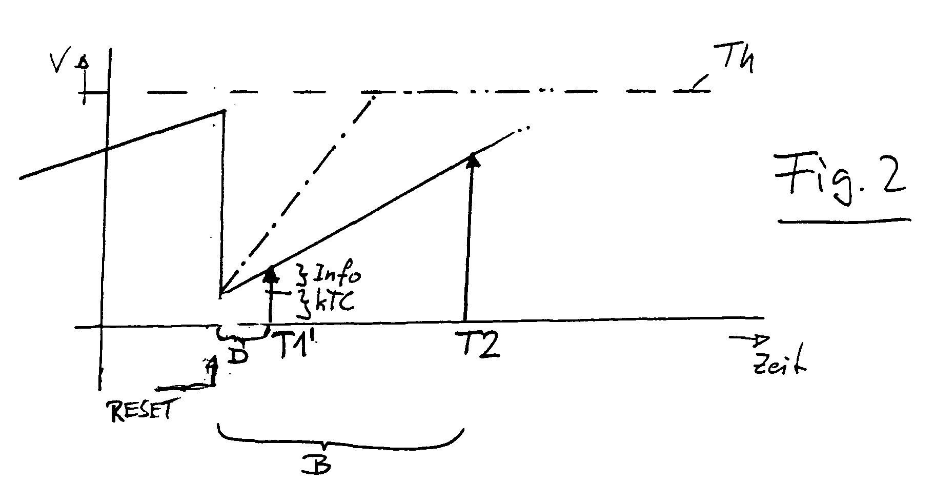
- FIG. 2 shows a scanning process in detail.
- CDS method Correlated Double Sampling
- a charge accumulates in one of the pixels a capacitor, not shown here, converted into a voltage V. becomes.
- the CMOS image sensor 2 of Figure 1 by one of the Controller 8 output RESET pulse reset pixel by pixel.
- the voltage V drops in accordance with FIG. 3 abruptly to a certain value, which is designated here with kTC and mainly corresponds to the noise signal amplitude to the RESET noise.
- the time now rises T1 continues to sense voltage V already sensed for the first time, depending the brightness to which the pixel is exposed.
- Exposure period B is a second sample of the voltage V to a point in time T2.
- the signal amplitude at time T2 is also afflicted with the noise signal amplitude kTC.
- the pixel under consideration is also by the RESET pulse reset so that the voltage value to a noise signal amplitude decreases, also designated kTC in FIG.
- the first scan takes place not at or immediately after the RESET pulse, but around a predetermined delay period D is delayed at the time T1 '.
- the exposure of the pixel has already changed a certain amount of charge accumulated, that of a certain voltage corresponds to "Info" in FIG. 2 in order to clarify that the signal sampled at time T1 'information about the brightness contains.
- the correction is made by subtracting the samples at T2 and T1 ', the difference signal obtained is from Noise signal component kTC exempt, but is compared to that in Figure 3 case slightly lower, namely by the value that in Figure 2 is labeled "Info".
- output A in FIG a difference signal formed by subtracting the first sample at T1 'from the second sample at T2', or a signal which is obtained from only the first sample at T1 '.
- the switch 12 shown in Figure 1 enables only the two alternatives “Differential signal” on the one hand or "derived from the first sample Useful signal "on the other hand.
- the switch 12 according to FIG. 1 can be replaced by a circuit, which is a smooth transition between the two operating modes mentioned allows.
- a circuit which is a smooth transition between the two operating modes mentioned allows.
- a weighted average be formed with the weight near the area low brightness for the "difference signal” is greater than for that useful signal derived from the first sample. Near the area the brightness distribution is then reversed. hereby you get a smooth transition between the two modes.
Landscapes
- Engineering & Computer Science (AREA)
- Multimedia (AREA)
- Signal Processing (AREA)
- Transforming Light Signals Into Electric Signals (AREA)
- Solid State Image Pick-Up Elements (AREA)
Abstract
Bei einem CMOS-Bildsensor wird zur Verminderung des RESET-Rauschens
ein korreliertes Doppelabtasten (Correlated Double Sampling;
CDS) durchgeführt: für die Pixel erfolgt nach dem RESET das Erfassen
eines ersten Abtastsignals, am Ende eines Belichtungszeitraums wird ein
zweiter Abtastwert ermittelt, und es wird ein von dem RESET-Rauschen
im wesentlichen befreites Differenzsignal gebildet, indem von dem zweiten
Abtastwert der erste Abtastwert subtrahiert wird. Um die mangelhafte
Helligkeitsdynamik zu verbessern, wird erfindungsgemäß das erste
Abtastsignal erst nach einem gewissen Verzögerungsintervall gewonnen,
so daß auch dieses Signal nicht nur eine Rauschkomponente, sondern
auch Helligkeitsinformation enthält. Übersteigt das zweite Abtastsignal
die Sättigungsgrenze, so wird als Nutzsignal lediglich das entsprechend
skalierte erste Abtastsignal hergenommen. Zwar ist in diesem Fall das
Nutzsignal mit dem RESET-Rauschen behaftet, allerdings fällt dieses bei
großen Helligkeiten kaum ins Gewicht. Man erzielt eine Vervielfachung
der Helligkeitsdynamik eines CMOS-Bildsensors.
Description
Die Erfindung betrifft eine Digitalkamera mit einem CMOS-Bildsensor mit einer Mehrzahl von Pixeln, die innerhalb eines Belichtungszeitraums jeweils eine von der Helligkeit abhängige Ladung speichern, die unter Steuerung durch eine Steuereinrichtung als Pixelsignal ausgegeben wird, mit einer Korrektureinrichtung, die nach einem Pixel-RESET des Bildsensors aus einem gegen Anfang und einem gegen Ende des Belichtungszeitraums für die Pixel erfaßten ersten bzw. zweiten Abtastwert die Differenz bildet und den um den ersten Abtastwert verminderten zweiten Abtastwert als Nutzsignal ausgibt.The invention relates to a digital camera with a CMOS image sensor with a plurality of pixels within one exposure period each store a charge dependent on the brightness, the under Control is output by a control device as a pixel signal, with a correction device after a pixel RESET of the image sensor one towards the beginning and one towards the end of the exposure period the first and second sample values acquired for the pixels Difference forms and the second reduced by the first sample Outputs the sample as a useful signal.
Außerdem betrifft die Erfindung ein Verfahren zum Ansteuern eines CMOS-Bildsensors.The invention also relates to a method for actuating a CMOS image sensor.
Für beispielsweise digitale Kameras und dergleichen sind CCD-Bildsensoren seit längerer Zeit bekannt. Es gibt ferner CMOS-Bildsensoren, die aber gegenüber CCD-Bildsensoren eine schlechtere Helligkeitsdynamik aufweisen. Unter dem Begriff Helligkeitsdynamik versteht man das Verhältnis aus Sättigungssignalamplitude des belichteten Bildsensors und seiner Rauschsignalamplitude bei unbelichtetem Sensor. Wenn an dieser Stelle nichts anderes gesagt ist, so betreffen die Anmerkungen ein beliebiges Pixel des Bildsensors, bei dem eine Vielzahl von Pixeln in Reihen und Spalten angeordnet ist. For example, digital cameras and the like are CCD image sensors known for a long time. There are also CMOS image sensors that but poorer brightness dynamics compared to CCD image sensors exhibit. The term brightness dynamics means that Ratio of the saturation signal amplitude of the exposed image sensor and its noise signal amplitude when the sensor is not exposed. If at this If nothing else is said, the comments concern any one Pixel of the image sensor, in which a large number of pixels in rows and columns is arranged.
Bei den hier in Rede stehenden Bildsensoren wird in jedem Pixel des Bildsensors eine gewisse Ladungsmenge innerhalb eines bestimmten Belichtungszeitraums angesammelt. Die Ladung wird mit Hilfe eines Kondensators in eine Spannung umgesetzt. Die von einem Pixel aufnehmbare Ladungsmenge ist nach oben begrenzt. Bei vorgegebenem Belichtungszeitraum gibt es eine gewisse Helligkeit, bei der die angesammelte Ladungsmenge gerade die Obergrenze erreicht. Bei größerer Helligkeit wird die Obergrenze für die ansammelbare Ladungsmenge bereits früher erreicht, so daß der am Ende des Belichtungszeitraums erhaltene Pegel des Nutzsignals nicht mehr aussagekräftig über die aufgenommene Lichtmenge ist.In the image sensors in question, the Image sensor a certain amount of charge within a certain Exposure period accumulated. The cargo is transported using a Capacitor converted into a voltage. The one-pixel recordable The amount of charge is limited. With given Exposure period there is a certain brightness at which the accumulated Amount of charge just reached the upper limit. At higher brightness the upper limit for the amount of charge that can be accumulated already reached earlier so that the one obtained at the end of the exposure period Level of the useful signal is no longer meaningful about the recorded Amount of light is.
Es gibt mehrere Rauschquellen für einen unbelichteten Sensor. Neben dem (thermischen) Systemrauschen und dem Dunkelstromrauschen gibt es noch das sogenannte RESET-Rauschen, auch als kTC-Rauschen oder kTC-Noise bekannt. Zu Beginn eines Belichtungszeitraumes wird auf die Pixel ein RESET-Signal gegeben, welches bis dahin in dem Pixel gespeicherte Ladungen ableitet. Aber auch unmittelbar nach einem RESET-Vorgang liefert das betreffende Pixel ein Signal, nämlich das Rauschsignal. Dieses kTC-Rauschen stellt den überwiegenden Rauschanteil dar. Bei CMOS-Bildsensoren kommt noch das Umschaltrauschen des Spalten-Multiplexers hinzu. Bei einem belichteten Sensor kommt noch das Photonenrauschen hinzu.There are several sources of noise for an unexposed sensor. Next the (thermal) system noise and the dark current noise it is the so-called RESET noise, also known as kTC noise or Known kTC noise. At the beginning of an exposure period, the Pixel is given a RESET signal, which was previously stored in the pixel Derives charges. But also immediately after a RESET process the pixel in question provides a signal, namely the noise signal. This kTC noise represents the predominant noise component. With CMOS image sensors there is also the switching noise of the column multiplexer added. With an exposed sensor comes the photon noise added.
Zusätzlich zu den genannten Rauschsignalen kommt bei einem CMOS-Bildsensor noch eine zeitlich konstante Störquelle hinzu. Diese hat die Form von Dunkelwert-Offsets. Nicht ganz korrekt wird diese Störung häufig auch als "fixed pattern noise" bezeichnet, wenngleich es sich nicht um eine statistische Störquelle, sondern um eine zeitlich konstante Störquelle handelt. Diese Störungen sind von Pixel zu Pixel unterschiedlich und lassen sich in einfacher Weise berücksichtigen, wie unten näher ausgeführt wird.In addition to the noise signals mentioned, there is a CMOS image sensor a constant source of interference. This has the Form of dark value offsets. This disorder is not entirely correct often referred to as "fixed pattern noise", although it is not a statistical source of interference, but a constant source of interference over time is. These disturbances differ from pixel to pixel and can be easily taken into account, as detailed below is performed.
Um eine Verfälschung des Nutzsignals bei Bildsensoren durch das RESET-Rauschen zu unterdrücken, ist es bekannt, den am Ende des Belichtungszeitraums gewonnenen Signal-Abtastwert zu korrigieren, indem man von diesem Abtastwert einen Rausch-Abtastwert subtrahiert. Zu diesem Zweck wird direkt nach dem RESET-Signal ein erster Abtastwert gewonnen, der in erster Linie dem RESET-Rauschen entspricht. Von dem am Ende des Belichtungszeitraums gewonnenen zweiten Abtastwert wird dann der erste Abtastwert subtrahiert. Da beide Abtastwerte mit dem gleichen RESET-Rauschen behaftet sind, ist das Differenzsignal im wesentlichen von dem RESET-Rauschen befreit.To falsify the useful signal in image sensors due to the RESET noise to suppress it is known to occur at the end of the exposure period correct the signal sample obtained by using subtracts a noise sample from this sample. To this For this purpose, a first sample value is obtained directly after the RESET signal, which corresponds primarily to the RESET noise. From the on Second sample obtained at the end of the exposure period then subtract the first sample. Since both samples with the same RESET noise, the difference signal is in essentially freed from the RESET noise.
Zum Stand der Technik wird zum Beispiel auf die US-Patentschriften 5 742 047; 6 111 242; 6 115 066 und 5 877 715 verwiesen. Das oben beschriebene Verfahren der Differenzbildung zur Korrektur des Nutzsignals ist dort auch für CMOS-Bildsensoren beschrieben. Man kann die Subtraktion anhand von Analogsignalen durchführen, möglich ist aber auch ein digitales Verarbeiten der Signale, insbesondere bei CMOS-Bildsensoren, da bei diesen Sensoren für jedes Pixel ein eigener Ladungs-Spannungs-Wandlerkondensator vorhanden ist. Zweckmäßig ist dann ein Bildspeicher zur Speicherung der gesamten Dunkelbildinformation für alle Pixel in digitaler Form. Das mit Hilfe eines Analog-Digital-Wandlers digitalisierte gespeicherte Dunkelbild wird dann pixelweise von dem digitalen Bild entsprechend der am Ende des Belichtungszeitraums durchgeführten Abtastung subtrahiert. The prior art is referred to, for example, US Pat. No. 5 742 047; 6,111,242; 6 115 066 and 5 877 715. The above described method of difference formation for correcting the useful signal is also described there for CMOS image sensors. You can do that Carry out subtraction using analog signals, but is possible also digital processing of the signals, especially in the case of CMOS image sensors, because with these sensors there is a separate charge-voltage converter capacitor for each pixel is available. Is expedient then an image memory for storing all of the dark image information for all pixels in digital form. With the help of an analog-digital converter digitized stored dark image is then pixel by pixel the digital image corresponding to that at the end of the exposure period performed subtracted.
Das oben angesprochene Verfahren mit Korrektur durch Subtraktion zweier Abtastwerte ist aus dem Stand der Technik bekannt, es wird dort mit Correlated Double Sampling (CDS) bezeichnet. Aus dem angegebenen Stand der Technik ist dieses CDS-Verfahren für CMOS-Bildsensoren bereits bekannt. Allerdings ist der für das digitale CDS-Verfahren erforderliche Aufwand derart groß, daß man üblicherweise darauf verzichtet. Aus diesem Grund haben bildgebende Systeme mit CMOS-Sensoren den Ruf geringer Dynamik.The method mentioned above with correction by subtraction two samples are known from the prior art, it is there referred to as Correlated Double Sampling (CDS). From the specified This CDS method for CMOS image sensors is state of the art already known. However, that is required for the digital CDS process The effort is so great that you usually do without it. For this reason, imaging systems with CMOS sensors have the Reputation of low dynamics.
Der Erfindung liegt die Aufgabe zugrunde, eine Digitalkamera der eingangs genannten Art anzugeben, die eine im Vergleich zum Stand der Technik gesteigerte Helligkeitsdynamik besitzt.The invention has for its object a digital camera of the beginning specified type, which is a compared to the status of Technology has increased brightness dynamics.
Außerdem soll ein Verfahren angegeben werden, das eine Voraussetzung für die Verbesserung der Dynamik eines CMOS-Bildsensors schafft.In addition, a procedure is to be specified that is a prerequisite for improving the dynamics of a CMOS image sensor.
Bei einer Digitalkamera der oben genannten Art wird dies dadurch erreicht, daß die Steuereinrichtung die Abtastung für den ersten Abtastwert gegenüber dem RESET um eine vorgegebene Verzögerungszeitspanne verzögert.With a digital camera of the type mentioned above, this is achieved by that the controller scans for the first sample compared to the RESET by a predetermined delay period delayed.
Die Erfindung basiert auf einigen grundlegenden Erkenntnissen, die im folgenden näher diskutiert werden sollen:The invention is based on some basic knowledge, which in the following should be discussed in more detail:
Erstens: im Stand der Technik wird davon ausgegangen, daß mit dem ersten Abtastwert ein bloßes Rausch-Signal gewonnen wird, welches keinerlei Bildinformation enthält, und daß man durch Subtrahieren dieses reinen Rausch-Signals von dem zweiten Abtastwert dann im wesentlichen die reine Bildinformation erhält. Das durch kTC-Noise verursachte Rausch-Signal ist ein Zufallssignal, welches eine beim RESET-Vorgang eingefrorene Amplitude hat, die während des gesamten nachfolgenden Belichtungszeitraums unverändert bleibt. Dementsprechend enthält also auch ein gegenüber dem RESET verzögert gewonnenes erstes Abtastsignal exakt den durch kTC-Rauschen verursachten Rauschsignalanteil, der dem im RESET-Zeitpunkt gewonnenen Rausch-Signal entspricht. Durch Subtrahieren des - erfindungsgemäß gegenüber dem RESET verzögert gewonnenen - ersten Abtastsignals von dem zweiten Abtastsignal erhält man also ebenfalls ein von dem kTC-Rauschen befreites Nutzsignal.First: in the prior art it is assumed that with the first sample, a mere noise signal is obtained, which contains no image information, and that by subtracting this pure noise signal from the second sample then essentially receives the pure image information. That caused by kTC noise Noise signal is a random signal, which one during the RESET process has frozen amplitude throughout the subsequent Exposure period remains unchanged. Accordingly, contains also a first sampling signal obtained with a delay compared to the RESET exactly the amount of noise signal caused by kTC noise, the corresponds to the noise signal obtained at the RESET time. By Subtract the - delayed according to the RESET obtained - receives the first scanning signal from the second scanning signal a useful signal also freed from the kTC noise.
Der in dem verzögert gewonnenen ersten Abtastsignal enthaltene Bildanteil geht zwar bei dem Subtraktionsvorgang verloren, jedoch ist dieser Verlust vernachlässigbar im Hinblick auf die vervielfachte Helligkeitsdynamik, wie weiter unten noch näher ausgeführt wird.The image component contained in the delayed first sampling signal is lost in the subtraction process, but it is Loss negligible with regard to the multiplied brightness dynamics, as will be explained in more detail below.
Zweitens: wie oben erwähnt, kommt bei einem belichteten Bildsensor zu den verschiedenen Rauschanteilen noch das Photonenrauschen hinzu. Bei starker Helligkeit, insbesondere bei Helligkeiten, bei denen der CMOS-Bildsensor zur Sättigung neigt, ist der Anteil des Photonenrauschens derart groß, daß demgegenüber das - von der Helligkeit unabhängige - kTC-Rauschen untergeht. Aus diesem Grund spielt das kTC-Rauschen bei Bildsignalen, die durch große Helligkeit zustandekommen, eine untergeordnete Bedeutung.Second, as mentioned above, an exposed image sensor is important add the photon noise to the different noise components. at strong brightness, especially when the CMOS image sensor tends to be saturated, is the proportion of photon noise so large that, in contrast, the - independent of the brightness - kTC noise goes down. For this reason, the kTC noise plays a lower level for image signals that are created by high brightness Importance.
Wenn man von dem am Ende des Belichtungszeitraums gewonnenen zweiten Abtastwert den ersten Abtastwert subtrahiert, so erhält man zwar ein von dem RESET-Rauschen befreites Signal, allerdings ist dieses Signal im Vergleich zum Stand der Technik, bei dem der erste Abtastwert unmittelbar nach dem RESET erfaßt wird, etwas verringert, und zwar um die Bildinformations-Komponente. Wenn man - wie in einer bevorzugten Ausführungsform der Erfindung vorgesehen - die Verzögerungszeitspanne so wählt, daß sie etwa 1% bis 20%, vorzugsweise 2% bis 10% des gesamten Belichtungszeitraums entspricht, so verringert sich im Normalbetrieb die Amplitude des Nutzsignals aufgrund der Subtraktion um etwa diesen prozentualen Anteil.If one of the ones obtained at the end of the exposure period second sample subtracts the first sample, you get a signal freed from the RESET noise, but this is Signal compared to the prior art, in which the first sample immediately after the RESET is detected, slightly decreased, and namely the image information component. If you - like in a preferred embodiment of the invention provided - the delay period so chosen that it is about 1% to 20%, preferably 2% corresponds to up to 10% of the entire exposure period, so decreases in normal operation the amplitude of the useful signal due to the subtraction by about this percentage.
Im Gegenzug wird allerdings ein erheblicher Vorteil erreicht, nämlich eine vergrößerte Helligkeitsdynamik des Bildsensors. Wenn bei großer Helligkeit ein Pixel sehr schnell in Sättigung geht, das heißt seine obere mögliche Ladungsgrenze erreicht, so ist das von diesem Pixel stammende Nutzsignal unbrauchbar, da das Sättigungssignal praktisch keine Information mehr darüber enthält, wie stark die Belichtung innerhalb der Belichtungszeitspanne war.In return, however, a significant advantage is achieved, namely an increased brightness dynamic of the image sensor. If large Brightness a pixel goes into saturation very quickly, that is its top possible charge limit is reached, then this is from this pixel Usable signal useless, since the saturation signal practically no information contains more about how strong the exposure is within the exposure period was.
Erfindungsgemäß kann in solchen Situationen das erste Abtastsignal als Informationsquelle herangezogen werden. Zwar ist das erste Abtastsignal noch mit dem - bei großen Helligkeiten vernachlässigbaren-RESET-Rauschen behaftet, allerdings enthält es auch einen Informationssignalanteil, wobei die Signalamplitude dadurch verfälscht ist, daß der Belichtungszeitraum für das erste Abtastsignal nur der Verzögerungszeitspanne entspricht. Da der ursprüngliche Belichtungszeitraum einerseits und die Verzögerungszeitspanne andererseits jedoch bekannt sind, kann man das erste Abtastsignal mit einem entsprechenden Faktor multiplizieren, um so den ersten Abtastwert auf einen Wert zu extrapolieren, der einem Signal bei voller ursprünglicher Belichtungszeit entspricht.According to the invention, the first scanning signal can be used in such situations as Source of information. It is true that the first scanning signal still with the - negligible at high brightness RESET noise afflicted, but it also contains an information signal component, the signal amplitude is falsified by the fact that the exposure period for the first scan signal only the delay period equivalent. Because the original exposure period on the one hand and the Delay time span on the other hand are known, you can do that multiply the first scanning signal by a corresponding factor, so extrapolate the first sample to a value corresponding to a signal at full original exposure time.
Die obigen Betrachtungen zeigen auch, daß man wegen der geringen Signalamplitude des ersten Absatzwerts einen erheblichen Spielraum hat, bis zu dem hin man dieses erste Abtastsignal auch bei extrem großen Helligkeiten als Informationssignal nutzen kann. Wenn die Verzögerungszeitspanne zum Beispiel 10% des eigentlichen Belichtungszeitraums entspricht, so kann man unter der Annahme, daß der zweite Abtastwert gerade der Sättigungssignalamplitude entspricht, die Helligkeitsdynamik des Bildsensors um circa den Faktor 10 verbessern. Erst bei einer derart starken Helligkeit würde auch der erste Abtastwert die Sättigungsgrenze erreichen.The above considerations also show that because of the small Signal amplitude of the first sales value has considerable scope, up to which you can get this first scanning signal even with extremely large ones Can use brightness as an information signal. If the delay period for example 10% of the actual exposure period corresponds, so one can assume that the second sample corresponds exactly to the saturation signal amplitude, the brightness dynamics the image sensor by about a factor of 10. Only at; only when Such a high brightness would also make the first sample the saturation limit to reach.
Um den ersten Abtastwert in einer bevorzugten Ausgestaltung der Erfindung tatsächlich nutzen zu können, kann man den zweiten Abtastwert mit einem Schwellenwert vergleichen. Ist der Abtastwert höher als der Schwellenwert, kann man den ersten Abtastwert mit einem entsprechenden Skalierungs-Faktor (abgeleitet von dem Verhältnis des eigentlichen Belichtungszeitraums zu der Verzögerungszeitspanne) multiplizieren und den so gewonnenen Wert als Nutzsignal hernehmen.Around the first sample in a preferred embodiment of the invention to actually be able to use the second sample with compare to a threshold. If the sample is higher than that Threshold, you can get the first sample with a corresponding one Scaling factor (derived from the ratio of the actual Multiply the exposure period by the delay period) and take the value obtained in this way as a useful signal.
Alternativ kann man aus dem ersten Abtastwert unter Heranziehung des Skalierungs-Faktors einen Erwartungswert für den zweiten Abtastwert ermitteln. Wenn dieser Erwartungswert über einem gewissen Schwellenwert liegt, kann man dann aus dem ersten Abtastwert in der oben beschriebenen Weise das Nutzsignal ermitteln.Alternatively, one can from the first sample using the Scaling factor an expected value for the second sample determine. If this expected value is above a certain threshold is then from the first sample in the one described above Determine the useful signal.
Die erfindungsgemäße Digitalkamera kann also - bei geringen und mittleren
Helligkeiten - einerseits wie eine herkömmliche Kamera arbeiten,
sie arbeitet - bei mittleren und größeren Helligkeiten - in einer neuen
Betriebsweise, bei der das durch das CDS-Verfahren ermittelte Nutzsignal
ersetzt wird durch ein nur aus dem ersten Abtastwert abgeleitetes
Nutzsignal.
In der Praxis kann es möglicherweise zu unerwünschten Bildkanten oder
-stufen kommen, nämlich dann, wenn ein plötzlicher Übergang von der
einen zur anderen Betriebsweise stattfindet. Aus diesem Grund ist erfindungsgemäß
vorgesehen, daß der Übergang zwischen den beiden oben
erwähnten Betriebsarten allmählich oder fließend erfolgt. Dementsprechend
wird abhängig von der aus dem ersten und/oder dem zweiten
Abtastwert hergeleiteten Helligkeit als Nutzsignal ausgegeben:
Das oben angesprochene "fixed pattern noise", welches genau genommen eine zeitlich konstante Störquelle und kein statistisches Rauschen darstellt, wird erfindungsgemäß dadurch berücksichtigt, daß ein Dunkelwert-Offset-Speicher vorgesehen ist, und daß von dem ersten Abtastwert eines jeweiligen Pixels ein zu diesem Pixel gehöriger, in dem Dunkelwert-Offset-Speicher vorab gespeicherter Offsetwert subtrahiert wird. Man kann einmal vor Inbetriebnahme der Digitalkamera durch Aufnahme bei unbelichtetem Sensor für die Pixel des CMOS-Bildsensors die Offset-Werte speichern, um sie dann bei jeder Bildausgabe von den ersten Abtastwerten entsprechender Pixel zu subtrahieren. Das Speichern der Dunkelwert-Offsets läßt sich auch von Zeit zu Zeit wiederholen um die Werte zu aktualisieren. The "fixed pattern noise" mentioned above, which is strictly speaking represents a constant source of interference and no statistical noise, is taken into account according to the invention in that a dark value offset memory is provided, and that of the first sample one a pixel belonging to this pixel in the dark value offset memory previously stored offset value is subtracted. you can be taken once before putting the digital camera into operation unexposed sensor for the pixels of the CMOS image sensor the offset values then save them each time the image is output from the first Subtract samples of corresponding pixels. Saving the Dark value offsets can also be repeated from time to time Update values.
Die Erfindung schafft außerdem ein Verfahren zum Ansteuern eines CMOS-Bildsensors nach dem sogenannten CDS-Verfahren, bei dem Pixel des Bildsensors gegen Anfang und gegen Ende eines Belichtungszeitraums abgetastet werden, und durch Subtrahieren des ersten Abtastwerts von dem zweiten Abtastwert ein Nutzsignal gewonnen wird, wobei erfindungsgemäß vorgesehen ist, daß der erste Abtastwert gegenüber dem RESET nach einer vorbestimmten Verzögerungszeitspanne mit verwertbarer Bildinformation gewonnen wird.The invention also provides a method of driving a CMOS image sensor according to the so-called CDS process, in which Pixel of the image sensor towards the beginning and towards the end of an exposure period are sampled, and by subtracting the first sample a useful signal is obtained from the second sample, wherein it is provided according to the invention that the first sample value is opposite the RESET after a predetermined delay period usable image information is obtained.
Im folgenden wird ein Ausführungsbeispiel der Erfindung anhand der
Zeichnung näher erläutert. Es zeigen:
Figur 1 zeigt eine elektrische Schaltung 1 einer Digitalkamera mit einem
CMOS-Bildsensor 2, der von einer Steuereinrichtung 8 gesteuert wird,
und dem ein Analog-Digital-Wandler 4 nachgeschaltet ist. Der Analog-Digital-Wandler
4 setzt die Analogsignale vom Ausgang des CMOS-Bildsensors
2 in Digitalwerte um, die dann unter Steuerung durch die
Steuereinrichtung 8 in einem Dunkelbild-Speicher 10 gespeichert werden.
Die gespeicherten Werte in dem Dunkelbild-Speicher 10 entsprechen den
digitalisierten Spannungswerten für die einzelnen Pixel des CMOS-Sensorelements
2. Diese Spannungswerte werden nach einem RESET-Signal
durch eine erste Abtastung gewonnen, gesteuert durch die Steuereinrichtung
8.Figure 1 shows an electrical circuit 1 of a digital camera with a
Die bei einer zweiten Abtastung am Ende eines Belichtungszeitraums
gewonnenen und digitalisierten Abtastwerte werden von dem Subtrahierer
6 zu einem Differenzsignal gebildet, indem die in dem Dunkelbild-Speicher
10 gespeicherten ersten Abtastwerte pixelweise und digital von den
digitalen zweiten Abtastwerten subtrahiert werden, wiederum unter
Steuerung durch die Steuereinrichtung 8. Das Differenzsignal am Ausgang
des Subtrahierers 6 wird über einen ersten Eingang eines Schalters
12 einem Nutzsignal-Ausgang A zugeleitet.The one at a second scan at the end of an exposure period
obtained and digitized samples are taken from the subtractor
6 to a difference signal formed by those in the
Die in dem Dunkelbild-Speicher 10 gespeicherten ersten Abtastwerte
werden außerdem einem Multiplizierer 14 zugeleitet, wo die Abtastwerte
mit einem Skalierungs-Faktor F multipliziert werden.The first samples stored in the
Vor dem Multiplizieren wird jeder Pixelwert aus dem Dunkelbild-Speicher
100 bezüglich des vorerwähnten "fixed pattern noise" korrigiert.
Hierzu werden in einem Dunkelwert-Offset-Speicher (11) für jedes Pixel
des CMOS-Bildsensors 2 vor der Inbetriebnahme der Digitalkamera
Offset-Werte gespeichert, die für die einzelnen Pixel des CMOS-Bildsensors
2 unterschiedlich sind. Bei jedem Auslesevorgang für den Bildspeicher
10 werden auch die Werte aus dem Dunkelwert-Offset-Speicher
synchron ausgelesen. Die Werte aus den Speichern 10 und 11 werden
von einem Subtrahierer 13 subtrahiert, und der Differenzwert, also der
von dem "fixed pattern noise" befreite erste Abtastwert aus dem Bildspeicher
10 wird dem Multiplizierer 14 zugeleitet, um mit dem Skalierungs-Faktor
F multipliziert zu werden.Before multiplying, each pixel value is removed from the dark image memory
100 corrected for the aforementioned "fixed pattern noise".
For this purpose, in a dark value offset memory (11) for each pixel
the
Die multiplizierten ersten Abtastwerte werden einem zweiten Eingang
des Schalters 12 zugeführt. Die Stellung des Schalters 12 wird von der
Steuereinrichtung 8 ausgewählt, abhängig von einem Erwartungswert für
den zweiten Abtastwert. Dieser Erwartungswert wird von der Steuereinrichtung
8 aus den jeweiligen ersten Abtastwerten errechnet. Ist die
Amplitude des jeweiligen ersten Abtastwerts so groß, daß von dem zweiten
Abtastwert erwartet werden kann, daß dieser über einem Sättigungs-Schwellenwert
Th liegt, so schaltet die Steuereinrichtung 8 den Schalter
12 in die untere Stellung, demzufolge am Nutzsignal-Ausgang A ein
Nutzsignal ausgegeben wird, welches durch Multiplizieren des ersten
Abtastwerts mit dem Faktor F gewonnen wird.The multiplied first samples become a second input
of the
Figur 2 zeigt einen Abtastvorgang im einzelnen. Bevor auf Figur 2 näher eingegangen wird, soll anhand der Figur 3 der Stand der Technik erläutert werden. Es wird hier insbesondere Bezug genommen auf die eingangs genannten US-Patentschriften, die hier als durch Bezugnahme inkorporiert angesehen werden, insbesondere bezüglich des "Correlated Double Sampling"-Verfahrens (CDS-Verfahrens).Figure 2 shows a scanning process in detail. Before moving on to Figure 2 the state of the art will be explained with reference to FIG become. In particular, reference is made here to the above U.S. Patents referred to herein as by reference be considered incorporated, especially with regard to the "Correlated Double Sampling "method (CDS method).
Gemäß Figur 3 sammelt sich in einem der Pixel eine Ladung, die von
einem hier nicht dargestellten Kondensator in eine Spannung V umgesetzt
wird. Je größer die Helligkeit ist, welcher das betrachtete Pixel ausgesetzt
ist, desto steiler steigt die Spannung an. Zu einem gegebenen Zeitpunkt
wird der CMOS-Bildsensor 2 nach Figur 1 durch einen von der
Steuereinrichtung 8 ausgegebenen RESET-Impuls pixelweise zurückgesetzt.
Hierdurch werden sämtliche Restladungen aus den einzelnen Pixeln
abgeleitet.According to FIG. 3, a charge accumulates in one of the pixels
a capacitor, not shown here, converted into a voltage V.
becomes. The greater the brightness, which the viewed pixel is exposed to
the steeper the voltage rises. At a given time
is the
Aufgrund des RESET-Impulses sinkt die Spannung V gemäß Figur 3 schlagartig auf einen gewissen Wert ab, der hier mit kTC bezeichnet ist und der Rauschsignalamplitude entspricht, hauptsächlich zurückzuführen auf das RESET-Rauschen.Due to the RESET pulse, the voltage V drops in accordance with FIG. 3 abruptly to a certain value, which is designated here with kTC and mainly corresponds to the noise signal amplitude to the RESET noise.
Gemäß der durchgezogenen Linie in Figur 3 steigt nun die im Zeitpunkt T1 bereits zum ersten Mal abgetastete Spannung V weiter an, abhängig von der Helligkeit, der das Pixel ausgesetzt ist. Nach einem gegebenen Belichtungszeitraum B erfolgt eine zweite Abtastung der Spannung V zu einem Zeitpunkt T2. Die Signalamplitude im Zeitpunkt T2 ist ebenfalls mit der Rauschsignalamplitude kTC behaftet. Durch Subtraktion des bei T1 gewonnenen ersten Abtastwerts von dem bei T2 gewonnenen zweiten Abtastwert wird die Rauschsignalkomponente beseitigt.According to the solid line in FIG. 3, the time now rises T1 continues to sense voltage V already sensed for the first time, depending the brightness to which the pixel is exposed. After a given Exposure period B is a second sample of the voltage V to a point in time T2. The signal amplitude at time T2 is also afflicted with the noise signal amplitude kTC. By subtracting the T1 sampled first from the second sampled at T2 Sample, the noise signal component is eliminated.
Wie weiterhin in Figur 3 durch ein strichpunktierte Linie dargestellt ist, würde bei etwas erhöhter Helligkeit an dem betrachteten Pixel die Spannung nach etwa zwei Drittel des Belichtungszeitraums B bereits die Sättigungsgrenze Th erreichen. Ein zum Zeitpunkt T2 gewonnener Abtastwert wäre dann unbrauchbar.As further shown in FIG. 3 by a dash-dotted line, would the voltage at the pixel under consideration with somewhat increased brightness after about two thirds of the exposure period B the Reach the saturation limit Th. A sample obtained at time T2 would then be unusable.
Gemäß Figur 2 wird ebenfalls das betrachtete Pixel durch den RESET-Impuls zurückgesetzt, so daß der Spannungswert auf eine Rauschsignalamplitude abnimmt, in Figur 2 ebenfalls mit kTC bezeichnet.According to Figure 2, the pixel under consideration is also by the RESET pulse reset so that the voltage value to a noise signal amplitude decreases, also designated kTC in FIG.
Im Gegensatz zum Stand der Technik erfolgt aber die erste Abtastung nicht bei dem oder unmittelbar nach dem RESET-Impuls, sondern um eine vorbestimmte Verzögerungszeitspanne D verzögert im Zeitpunkt T1'. Zu diesem Zeitpunkt hat sich durch die Belichtung des Pixels bereits eine gewisse Ladungsmenge angesammelt, die einer gewissen Spannung entspricht, in Figur 2 mit "Info" bezeichnet, um zu verdeutlichen, daß das im Zeitpunkt T1' abgetastete Signal Information über die Helligkeit enthält.In contrast to the prior art, however, the first scan takes place not at or immediately after the RESET pulse, but around a predetermined delay period D is delayed at the time T1 '. At this point the exposure of the pixel has already changed a certain amount of charge accumulated, that of a certain voltage corresponds to "Info" in FIG. 2 in order to clarify that the signal sampled at time T1 'information about the brightness contains.
Wenn nun gemäß Figur 2 die Korrektur durch Subtraktion der Abtastwerte bei T2 und T1' erfolgt, ist das gewonnene Differenzsignal von der Rauschsignalkomponente kTC befreit, ist aber im Vergleich zu dem in Figur 3 dargestellten Fall etwas geringer, nämlich um den Wert, der in Figur 2 mit "Info" bezeichnet ist.If, according to FIG. 2, the correction is made by subtracting the samples at T2 and T1 ', the difference signal obtained is from Noise signal component kTC exempt, but is compared to that in Figure 3 case slightly lower, namely by the value that in Figure 2 is labeled "Info".
Es soll nun der Fall betrachtet werden, daß die Helligkeit an dem betreffenden Pixel so groß ist, daß die Signalspannung V entsprechend der strichpunktierten Linie sehr stark steigt. Das im Zeitpunkt T2 gewonnene zweite Abtastsignal wäre dann unbrauchbar. Erfindungsgemäß wird nun ausschließlich das im Zeitpunkt T1' erhaltene erste Abtastsignal als Nutzsignal verwendet. Es erfolgt eine Multiplikation mit einem Skalierungsfaktor F, der etwa den Wert B/D besitzt, um den Umstand zu berücksichtigen, daß die Belichtungszeit im Zeitpunkt T1' gegenüber der eigentlichen Belichtungszeit stark verkürzt ist und diese Verkürzung kompensiert werden muß.Let us now consider the case where the brightness of the subject Pixel is so large that the signal voltage V corresponding to the dash-dotted line rises very sharply. The one obtained at time T2 the second scanning signal would then be unusable. According to the invention only the first scanning signal received at time T1 'as Useful signal used. It is multiplied by a scaling factor F, which has approximately the value B / D, to the circumstance take into account that the exposure time at time T1 'compared to actual exposure time is greatly shortened and this shortening must be compensated.
Am Ausgang A in Figur 1 erhält man also je nach Helligkeit entweder ein Differenzsignal, gebildet durch Subtrahieren des ersten Abtastwerts bei T1' von dem zweiten Abtastwert bei T2', oder ein Signal, welches aus lediglich dem ersten Abtastwert bei T1' gewonnen wird. Depending on the brightness, output A in FIG a difference signal formed by subtracting the first sample at T1 'from the second sample at T2', or a signal which is obtained from only the first sample at T1 '.
Aus Figur 2 ist ersichtlich, daß die Helligkeitsdynamik des Bildsensors gemäß der Erfindung im Vergleich zum Stand der Technik um ein Vielfaches verbessert ist; denn die Spannung V müßte extrem steil ansteigen, um bis zu dem Zeitpunkt T1' der ersten Abtastung den oberen Sättigungswert Th zu erreichen.From Figure 2 it can be seen that the brightness dynamics of the image sensor according to the invention compared to the prior art many times over is improved; because the voltage V should rise extremely steep, by the time T1 'of the first scan the upper saturation value To reach th.
Der in Figur 1 dargestellte Schalter 12 ermöglicht nur die beiden Alternativen
"Differenzsignal" einerseits oder "aus erstem Abtastwert abgeleitetes
Nutzsignal" andererseits. Um Bildkanten oder -stufen zu vermeiden,
kann man den Schalter 12 nach Figur 1 durch eine Schaltung ersetzen,
welche einen fließenden Übergang zwischen den beiden genannten Betriebsarten
ermöglicht. In einem mittleren Helligkeitsbereich kann aus
den beiden Nutzsignal-Arten "Differenzsignal" einerseits und "aus erstem
Abtastwert hergeleitetes Nutzsignal" andererseits ein gewichteter Mittelwert
gebildet werden, wobei das Gewicht in der Nähe des Bereichs
geringer Helligkeit für das "Differenzsignal" größer ist als für das aus
dem ersten Abtastwert hergeleitete Nutzsignal. In der Nähe des Bereichs
großer Helligkeit ist die Gewichtsverteilung dann umgekehrt. Hierdurch
erhält man einen fließenden Übergang zwischen den beiden Betriebsarten.The
Claims (7)
Applications Claiming Priority (2)
| Application Number | Priority Date | Filing Date | Title |
|---|---|---|---|
| DE10110108A DE10110108A1 (en) | 2001-03-02 | 2001-03-02 | Digital camera with CMOS image sensor with improved dynamics and method for controlling a CMOS image sensor |
| DE10110108 | 2001-03-02 |
Publications (2)
| Publication Number | Publication Date |
|---|---|
| EP1237357A2 true EP1237357A2 (en) | 2002-09-04 |
| EP1237357A3 EP1237357A3 (en) | 2003-12-10 |
Family
ID=7676087
Family Applications (1)
| Application Number | Title | Priority Date | Filing Date |
|---|---|---|---|
| EP02004563A Withdrawn EP1237357A3 (en) | 2001-03-02 | 2002-02-27 | Digital camera with improved dynamic using CMOS image sensor and method for driving the CMOS image sensor |
Country Status (3)
| Country | Link |
|---|---|
| US (1) | US7221396B2 (en) |
| EP (1) | EP1237357A3 (en) |
| DE (1) | DE10110108A1 (en) |
Cited By (6)
| Publication number | Priority date | Publication date | Assignee | Title |
|---|---|---|---|---|
| WO2004074789A1 (en) * | 2003-02-17 | 2004-09-02 | Raytheon Company | Multi-mode dual integration detector circuit |
| DE10307744A1 (en) * | 2003-02-24 | 2004-09-02 | Carl Zeiss Jena Gmbh | Electromagnetic radiation intensity determination method in which measurements of radiation originating from particular locations are normalized based on the length of an intensity recording exposure |
| WO2007135161A1 (en) * | 2006-05-23 | 2007-11-29 | Thomson Licensing | Image sensor circuit |
| WO2010066850A1 (en) * | 2008-12-12 | 2010-06-17 | E2V Semiconductors | Image sensor with double charge transfer for large dynamic range and method of reading |
| CN110807812A (en) * | 2019-09-29 | 2020-02-18 | 浙江大学 | A system error calibration method for digital image sensor based on prior noise model |
| CN115684128A (en) * | 2022-10-28 | 2023-02-03 | 嘉庚创新实验室 | Raman spectrum signal noise reduction processing method and device and Raman spectrometer |
Families Citing this family (20)
| Publication number | Priority date | Publication date | Assignee | Title |
|---|---|---|---|---|
| US6963369B1 (en) * | 2002-04-01 | 2005-11-08 | Pixim, Inc. | Method for capturing and storing image information for multiple sampling operations in a digital pixel sensor |
| US6894264B2 (en) * | 2002-10-15 | 2005-05-17 | Applera Corporation | System and methods for dynamic range extension using variable length integration time sampling |
| US7480532B2 (en) * | 2003-10-22 | 2009-01-20 | Cvrx, Inc. | Baroreflex activation for pain control, sedation and sleep |
| JP4093220B2 (en) * | 2004-10-05 | 2008-06-04 | コニカミノルタホールディングス株式会社 | Solid-state imaging device and imaging device including the solid-state imaging device |
| US7554588B2 (en) * | 2005-02-01 | 2009-06-30 | TransChip Israel, Ltd. | Dual exposure for image sensor |
| US8081837B2 (en) * | 2006-02-07 | 2011-12-20 | Intel Corporation | Image sensor array leakage and dark current compensation |
| US7948532B2 (en) * | 2006-05-19 | 2011-05-24 | Jai Corporation | Solid-state image-pickup device signal processing apparatus with signal compensation circuit |
| JP2009538075A (en) * | 2006-05-24 | 2009-10-29 | トムソン ライセンシング | Circuit and method for reading and resetting pixels of an image sensor |
| US7969490B2 (en) | 2006-08-25 | 2011-06-28 | Micron Technology, Inc. | Method, apparatus, and system providing an imager with pixels having extended dynamic range |
| US7714903B2 (en) * | 2006-08-29 | 2010-05-11 | Zoran Corporation | Wide dynamic range image capturing system method and apparatus |
| US8687087B2 (en) * | 2006-08-29 | 2014-04-01 | Csr Technology Inc. | Digital camera with selectively increased dynamic range by control of parameters during image acquisition |
| US7791657B2 (en) * | 2007-03-07 | 2010-09-07 | Teledyne Licensing, Llc | Dynamic range enhancement scheme for imagers |
| US20090073293A1 (en) * | 2007-06-27 | 2009-03-19 | Yoel Yaffe | CMOS image sensors with increased dynamic range and methods of operating the same |
| US7948542B2 (en) * | 2007-07-05 | 2011-05-24 | Teledyne Licensing, Llc | Fast-settling line driver design for high resolution video IR and visible imagers |
| JP2009077345A (en) * | 2007-09-25 | 2009-04-09 | Olympus Corp | Solid-state imaging device |
| US9131142B2 (en) | 2009-07-17 | 2015-09-08 | Nikon Corporation | Focusing device and camera |
| DE102010050229A1 (en) | 2010-10-30 | 2012-05-03 | Viimagic Gmbh | Method for reading complementary metal oxide semiconductor image sensor with global shutter in digital camera for moving image recording, involves multiple reading of signal voltage buffered in pixel cell |
| US9965696B2 (en) * | 2015-12-31 | 2018-05-08 | James Alves | Digital camera control system |
| CN106961563B (en) * | 2017-03-24 | 2020-07-28 | 长春长光辰芯光电技术有限公司 | Low-noise wide-dynamic-range image sensor related multi-sampling circuit |
| CN115567789B (en) * | 2022-08-31 | 2023-12-12 | 成都微光集电科技有限公司 | Image signal processing method |
Family Cites Families (17)
| Publication number | Priority date | Publication date | Assignee | Title |
|---|---|---|---|---|
| US4399464A (en) * | 1981-05-04 | 1983-08-16 | General Dynamics, Pomona Division | Signal processor for an array of CID radiation detector elements |
| US4647975A (en) * | 1985-10-30 | 1987-03-03 | Polaroid Corporation | Exposure control system for an electronic imaging camera having increased dynamic range |
| US5162914A (en) * | 1987-06-09 | 1992-11-10 | Canon Kabushiki Kaisha | Image sensing device with diverse storage fumes used in picture composition |
| US5517242A (en) * | 1993-06-29 | 1996-05-14 | Kabushiki Kaisha Toyota Chuo Kenkyusho | Image sensing device having expanded dynamic range |
| DE69628187D1 (en) * | 1995-11-07 | 2003-06-18 | California Inst Of Techn | IMAGE SENSOR WITH LINEAR OUTPUT WITH LARGE DYNAMIC RANGE |
| US5742047A (en) * | 1996-10-01 | 1998-04-21 | Xerox Corporation | Highly uniform five volt CMOS image photodiode sensor array with improved contrast ratio and dynamic range |
| DE19742058C2 (en) * | 1996-11-15 | 2001-03-29 | Foveonics Inc | Method for operating an active pixel sensor cell |
| US5777715A (en) * | 1997-01-21 | 1998-07-07 | Allen Vision Systems, Inc. | Low vision rehabilitation system |
| US5877715A (en) | 1997-06-12 | 1999-03-02 | International Business Machines Corporation | Correlated double sampling with up/down counter |
| US6115066A (en) * | 1997-06-12 | 2000-09-05 | International Business Machines Corporation | Image sensor with direct digital correlated sampling |
| US6008486A (en) * | 1997-12-31 | 1999-12-28 | Gentex Corporation | Wide dynamic range optical sensor |
| US6111242A (en) * | 1998-01-02 | 2000-08-29 | Intel Corporation | Imaging system with gain and error correction circuitry |
| US6493030B1 (en) * | 1998-04-08 | 2002-12-10 | Pictos Technologies, Inc. | Low-noise active pixel sensor for imaging arrays with global reset |
| US7397506B2 (en) * | 1998-08-06 | 2008-07-08 | Intel Corporation | Reducing the effect of noise in an imaging system |
| JP4116254B2 (en) * | 1998-09-30 | 2008-07-09 | ミクロナス ゲゼルシャフト ミット ベシュレンクテル ハフツング | Method and apparatus for correcting exposure dependent noise in image sensors capable of addressing lines and columns |
| JP2002528970A (en) * | 1998-10-19 | 2002-09-03 | ベン−グリオン ユニバーシィティー オブ ザ ネゲブ | Optical imager using adaptive real-time extension of dynamic range |
| US6888572B1 (en) * | 2000-10-26 | 2005-05-03 | Rockwell Science Center, Llc | Compact active pixel with low-noise image formation |
-
2001
- 2001-03-02 DE DE10110108A patent/DE10110108A1/en not_active Ceased
-
2002
- 2002-02-27 EP EP02004563A patent/EP1237357A3/en not_active Withdrawn
- 2002-03-01 US US10/084,967 patent/US7221396B2/en not_active Expired - Fee Related
Cited By (9)
| Publication number | Priority date | Publication date | Assignee | Title |
|---|---|---|---|---|
| WO2004074789A1 (en) * | 2003-02-17 | 2004-09-02 | Raytheon Company | Multi-mode dual integration detector circuit |
| US7586074B2 (en) | 2003-02-17 | 2009-09-08 | Raytheon Company | Multi-mode high capacity dual integration direct injection detector input circuit |
| DE10307744A1 (en) * | 2003-02-24 | 2004-09-02 | Carl Zeiss Jena Gmbh | Electromagnetic radiation intensity determination method in which measurements of radiation originating from particular locations are normalized based on the length of an intensity recording exposure |
| WO2007135161A1 (en) * | 2006-05-23 | 2007-11-29 | Thomson Licensing | Image sensor circuit |
| WO2010066850A1 (en) * | 2008-12-12 | 2010-06-17 | E2V Semiconductors | Image sensor with double charge transfer for large dynamic range and method of reading |
| FR2939999A1 (en) * | 2008-12-12 | 2010-06-18 | E2V Semiconductors | DUAL LOAD TRANSFER IMAGE SENSOR FOR HIGH DYNAMIC AND READING METHOD |
| CN110807812A (en) * | 2019-09-29 | 2020-02-18 | 浙江大学 | A system error calibration method for digital image sensor based on prior noise model |
| CN110807812B (en) * | 2019-09-29 | 2022-04-05 | 浙江大学 | Digital image sensor system error calibration method based on prior noise model |
| CN115684128A (en) * | 2022-10-28 | 2023-02-03 | 嘉庚创新实验室 | Raman spectrum signal noise reduction processing method and device and Raman spectrometer |
Also Published As
| Publication number | Publication date |
|---|---|
| US20020122126A1 (en) | 2002-09-05 |
| US7221396B2 (en) | 2007-05-22 |
| DE10110108A1 (en) | 2002-09-19 |
| EP1237357A3 (en) | 2003-12-10 |
Similar Documents
| Publication | Publication Date | Title |
|---|---|---|
| EP1237357A2 (en) | Digital camera with improved dynamic using CMOS image sensor and method for driving the CMOS image sensor | |
| DE68928999T2 (en) | BROAD DYNAMIC CAMERA | |
| DE69920687T2 (en) | IMAGE SENSOR WITH EXTENDED DYNAMIC RANGE | |
| DE69625398T2 (en) | Black pattern correction for a charge transfer sensor | |
| DE60311107T2 (en) | LINEAR LOGARITHMIC ACTIVE PIXEL WITH GREAT DYNAMIC RANGE | |
| DE69616467T2 (en) | Solid-state image recording device with detection circuit of defective picture elements with high accuracy and low energy consumption | |
| DE69515833T2 (en) | Electronic camera with fast automatic focusing of the image on an image sensor | |
| DE69330151T2 (en) | Improved control of electronic shutter speed in a video camera | |
| DE69704896T2 (en) | Camera with digital and analog clamp circuit | |
| DE4041312C2 (en) | Electronic camera device for delivering an image signal with a wide dynamic range | |
| DE102009053281B4 (en) | image sensor | |
| DE3609887A1 (en) | CIRCUIT FOR THE ADAPTIVE CONTROL OF A RECURSIVE FILTER FOR VIDEO SIGNALS | |
| DE602005005553T2 (en) | Imaging device and imaging method | |
| DE102006011702A1 (en) | A system and method for subtracting dark noise from an image using an estimated dark noise scaling factor | |
| DE68915497T2 (en) | Endoscope with an adjustment device for the lighting ratio between a moving and a still image. | |
| DE112006003593B4 (en) | Image signal processing method and image signal processing device | |
| DE3542101A1 (en) | ARRANGEMENT FOR MEASURING THE DARK CURRENT IN SOLID-SCREEN CONVERTERS | |
| DE69910838T2 (en) | Reduction of streak-like interference in CMOS image sensors | |
| DE102010051986B4 (en) | Image sensor | |
| DE112004002663T5 (en) | Image subtraction of lighting artifacts | |
| EP2567539A1 (en) | Image sensor and method for recording an image | |
| DE69620572T2 (en) | CIRCUIT FOR DARK SHADING CORRECTION | |
| DE69119300T2 (en) | Color image capture device | |
| DE102011081405B4 (en) | Image sensor, imaging device and method for an image sensor | |
| DE69630074T2 (en) | Video device with a single multiport field memory |
Legal Events
| Date | Code | Title | Description |
|---|---|---|---|
| PUAI | Public reference made under article 153(3) epc to a published international application that has entered the european phase |
Free format text: ORIGINAL CODE: 0009012 |
|
| AK | Designated contracting states |
Kind code of ref document: A2 Designated state(s): AT BE CH CY DE DK ES FI FR GB GR IE IT LI LU MC NL PT SE TR |
|
| AX | Request for extension of the european patent |
Free format text: AL;LT;LV;MK;RO;SI |
|
| PUAL | Search report despatched |
Free format text: ORIGINAL CODE: 0009013 |
|
| AK | Designated contracting states |
Kind code of ref document: A3 Designated state(s): AT BE CH CY DE DK ES FI FR GB GR IE IT LI LU MC NL PT SE TR |
|
| AX | Request for extension of the european patent |
Extension state: AL LT LV MK RO SI |
|
| 17P | Request for examination filed |
Effective date: 20040609 |
|
| AKX | Designation fees paid |
Designated state(s): AT BE CH CY DE DK ES FI FR GB GR IE IT LI LU MC NL PT SE TR |
|
| 17Q | First examination report despatched |
Effective date: 20070531 |
|
| STAA | Information on the status of an ep patent application or granted ep patent |
Free format text: STATUS: THE APPLICATION IS DEEMED TO BE WITHDRAWN |
|
| 18D | Application deemed to be withdrawn |
Effective date: 20071011 |