EP1237267A2 - Converter - Google Patents
Converter Download PDFInfo
- Publication number
- EP1237267A2 EP1237267A2 EP02100196A EP02100196A EP1237267A2 EP 1237267 A2 EP1237267 A2 EP 1237267A2 EP 02100196 A EP02100196 A EP 02100196A EP 02100196 A EP02100196 A EP 02100196A EP 1237267 A2 EP1237267 A2 EP 1237267A2
- Authority
- EP
- European Patent Office
- Prior art keywords
- voltage
- circuit
- converter
- switching elements
- control signals
- Prior art date
- Legal status (The legal status is an assumption and is not a legal conclusion. Google has not performed a legal analysis and makes no representation as to the accuracy of the status listed.)
- Withdrawn
Links
- 230000003111 delayed effect Effects 0.000 claims description 8
- 239000003990 capacitor Substances 0.000 description 4
- 230000006978 adaptation Effects 0.000 description 2
- 230000001934 delay Effects 0.000 description 1
- 238000009499 grossing Methods 0.000 description 1
- 239000004065 semiconductor Substances 0.000 description 1
- 238000004804 winding Methods 0.000 description 1
Images

Classifications
-
- H—ELECTRICITY
- H02—GENERATION; CONVERSION OR DISTRIBUTION OF ELECTRIC POWER
- H02M—APPARATUS FOR CONVERSION BETWEEN AC AND AC, BETWEEN AC AND DC, OR BETWEEN DC AND DC, AND FOR USE WITH MAINS OR SIMILAR POWER SUPPLY SYSTEMS; CONVERSION OF DC OR AC INPUT POWER INTO SURGE OUTPUT POWER; CONTROL OR REGULATION THEREOF
- H02M3/00—Conversion of DC power input into DC power output
- H02M3/22—Conversion of DC power input into DC power output with intermediate conversion into AC
- H02M3/24—Conversion of DC power input into DC power output with intermediate conversion into AC by static converters
- H02M3/28—Conversion of DC power input into DC power output with intermediate conversion into AC by static converters using discharge tubes with control electrode or semiconductor devices with control electrode to produce the intermediate AC
- H02M3/325—Conversion of DC power input into DC power output with intermediate conversion into AC by static converters using discharge tubes with control electrode or semiconductor devices with control electrode to produce the intermediate AC using devices of a triode or a transistor type requiring continuous application of a control signal
- H02M3/335—Conversion of DC power input into DC power output with intermediate conversion into AC by static converters using discharge tubes with control electrode or semiconductor devices with control electrode to produce the intermediate AC using devices of a triode or a transistor type requiring continuous application of a control signal using semiconductor devices only
- H02M3/337—Conversion of DC power input into DC power output with intermediate conversion into AC by static converters using discharge tubes with control electrode or semiconductor devices with control electrode to produce the intermediate AC using devices of a triode or a transistor type requiring continuous application of a control signal using semiconductor devices only in push-pull configuration
- H02M3/3376—Conversion of DC power input into DC power output with intermediate conversion into AC by static converters using discharge tubes with control electrode or semiconductor devices with control electrode to produce the intermediate AC using devices of a triode or a transistor type requiring continuous application of a control signal using semiconductor devices only in push-pull configuration with automatic control of output voltage or current
-
- H—ELECTRICITY
- H02—GENERATION; CONVERSION OR DISTRIBUTION OF ELECTRIC POWER
- H02M—APPARATUS FOR CONVERSION BETWEEN AC AND AC, BETWEEN AC AND DC, OR BETWEEN DC AND DC, AND FOR USE WITH MAINS OR SIMILAR POWER SUPPLY SYSTEMS; CONVERSION OF DC OR AC INPUT POWER INTO SURGE OUTPUT POWER; CONTROL OR REGULATION THEREOF
- H02M3/00—Conversion of DC power input into DC power output
- H02M3/22—Conversion of DC power input into DC power output with intermediate conversion into AC
- H02M3/24—Conversion of DC power input into DC power output with intermediate conversion into AC by static converters
- H02M3/28—Conversion of DC power input into DC power output with intermediate conversion into AC by static converters using discharge tubes with control electrode or semiconductor devices with control electrode to produce the intermediate AC
-
- H—ELECTRICITY
- H02—GENERATION; CONVERSION OR DISTRIBUTION OF ELECTRIC POWER
- H02M—APPARATUS FOR CONVERSION BETWEEN AC AND AC, BETWEEN AC AND DC, OR BETWEEN DC AND DC, AND FOR USE WITH MAINS OR SIMILAR POWER SUPPLY SYSTEMS; CONVERSION OF DC OR AC INPUT POWER INTO SURGE OUTPUT POWER; CONTROL OR REGULATION THEREOF
- H02M1/00—Details of apparatus for conversion
- H02M1/0003—Details of control, feedback or regulation circuits
- H02M1/0012—Control circuits using digital or numerical techniques
Definitions
- the invention relates to a converter for converting a DC voltage (DC: direct current) into a DC output voltage, especially with TV or computer screens according to the preamble of claim 1.
- DC direct current
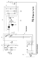
- Such a converter is known, for example, from US Pat. No. 5,777,859 with a data sheet for the high-performance resonance control devices MC 33067 and MC 34067 from Motorola Inc. from 1996 and in Fig. 6 shown.
- the converter of FIG. 6 comprises a first rectifier means 2 for converting an input voltage U in to a DC voltage U Bat.
- the rectifier device 2 is formed by a full-wave diode bridge rectifier 2-1 and a downstream smoothing capacitor C EL .
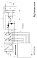
- the converter further comprises a bridge circuit 7 with controllable switching elements S1, S2 for converting the DC voltage U Bat into an AC voltage U ⁇ (AC: alternating current), which is switched by a downstream circuit 3 into an output DC voltage U out of the converter is transformed.
- AC alternating current
- the circuit 3 comprises a resonance power converter 3-1 and a second rectifier 3-2 connected downstream.
- the power converter 3-1 has a series circuit parallel to its input, which consists of a capacitor Cs and two coils Ls, Lp.
- the primary side of a transformer 13 with the primary number of turns n1 is connected in parallel with the coil Lp.
- the transformer On the secondary side, the transformer has n2 windings, to which a capacitor Cp is connected in parallel.
- a voltage across the capacitor Cp forms the output voltage of the power converter 3-1.
- the second rectifier 3-2 which is constructed analogously to the full rectifier 2, receives the output voltage of the power converter 3-1 at its input and generates the output voltage of the converter U out at its output.
- This DC output voltage U out is usually output to a load 17 which is connected to the converter.
- the converter further comprises a control circuit 5 'which generates the control signals in response to a first feedback signal which represents the magnitude of the DC output voltage U out of the converter.
- the efficiency of the resonance power converter 3-1 drops significantly when it is connected to input voltages, i.e. AC voltages U ⁇ is operated over a large voltage range are distributed; in this case there are undesirable losses in the Power converter 3-1 due to circulating reactive power.
- the full bridge circuit 7 comprises two parallel branches, each with two controllable switching elements S1 ... S4 connected in series.
- the input voltage DC voltage U Bat is fed to the full bridge circuit 7 in parallel with its branches, while it provides the AC voltage U ⁇ between the two switching elements of the two parallel branches.
- a control circuit 5 generates control signals for driving each of the controllable switching elements S1, S2 according to a first converter operating mode, hereinafter referred to as “half-bridge mode” or according to a second, hereinafter referred to as “full-bridge mode". Switching between the two modes is carried out by the control circuit 5 in accordance with a second feedback signal, which represents the magnitude of the DC voltage U Bat .
- the bridge circuit 7 operates in the full bridge mode with a phase edge of 180 °. In contrast, at higher DC voltages of, for example, 200 to 380 V, the bridge circuit 7 operates in the half-bridge mode.
- a corresponding switchover of the operating modes ensures that the value range of the input voltage AC voltage U ⁇ of the resonance power converter 3-1 is halved in a suitable manner compared to the pure DC voltage U Bat .
- the switchover from the full-bridge mode to the half-bridge mode or vice versa only during a dead time interval, during which at least one of the switching elements of the full-bridge circuit is load-free, i.e. switched off is.
- the converter has a first comparator circuit to generate a comparison signal as a binary signal according to the result of a comparison of the DC voltage with a first and a second Equivalent stress.
- This first comparator circuit is advantageously a Schmitt trigger formed which a hysteresis loop based on the first and the second Defined comparison voltage, whereby the generated comparison signal compared to smaller ones Fluctuations in the DC voltage is kept stable.
- controller has at least one adaptation circuit has, for performing a level adjustment of the control signals for the switching elements the full bridge circuit to predetermined level requirements.
- FIG. 1 essentially shows that already described above with reference to FIG. 7 Converter.
- the same reference numerals in the two figures denote the same components of the two converters.
- the converter according to the present invention and the known converter according to FIG. 7 differ, however, by the structure of the control circuit according to FIG. 5.
- the control circuit 5 comprises a first comparator circuit 32 for generating a binary comparison signal and a second comparator circuit 22 for generating a fourth control signal 24 for driving the switching element S4 and for generating a third control signal 25 to control the third switching element S3. All switching elements S1-S4 are preferably designed as power semiconductors.
- the control circuit 5 further comprises a logic circuit 34 for generating a delayed first control signal 35 for driving the first switching element S1 the full bridge circuit 7 and for generating a delayed second control signal 36 for driving the second switching element S2.
- the generation of the first and second Control signals 35, 36 are carried out by processing the third and fourth control signals, such as they are output from the second comparator circuit 22 in response to the binary comparison signal 33.
- the control circuit 5 further comprises a delay circuit 26 for delaying the third and fourth control signals by at least approximately a time period which corresponds to the processing time of a signal by the Logic circuit 34 corresponds, so that the respective control signals at the outputs of the Logic circuit 34 and the delay circuit 26 matched to one another in time are.
- the control circuit 5 also comprises two matching circuits 29 and 37 for performing level adjustment of the delayed first, second, third and / or fourth control signal to predetermined by the associated switching elements S1 ... S4 Level requirements.
- the DC voltage of the converter is applied to the inverting input of a first operational amplifier 32-1 and the non-inverting input of a second operational amplifier 32-2.
- the first operational amplifier 32-1 compares the DC voltage with a first predetermined reference voltage V ref 1 , which is present at its non-inverting input
- the second operational amplifier 32-2 compares the DC voltage with a second predetermined reference voltage V ref 2 , which is applied to its inverting input.
- the output of the second operational amplifier 32-2 is connected to an input of a NAND gate 32-3, on the second input of which the output of the first comparator circuit 32 is fed back.
- the output of this first NAND gate 32-3 forms, together with the output of the first operational amplifier 32-1, the inputs for a second NAND gate 32-4, the output of which also forms the output of the first comparator circuit 32.
- the circuit arrangement of the first comparator circuit 32 described forms a Schmitt trigger which defines a hysteresis loop via the two internal reference voltages V ref 1 , V ref 2 .
- the state and the changes in the DC input voltage U Bat are compared with the defined hysteresis loop.
- the binary comparison signal 33 is at the output of the first comparator circuit 32, on the basis of which a switchover between the operating modes of the full-bridge circuit 7 takes place.
- the full bridge circuit 7 switched to the full-bridge mode when the comparison signal 33 has assumed the binary value zero; on the other hand, the full bridge circuit 7 in switched to half-bridge mode when the binary comparison signal has the binary value 1 has accepted.
- the second comparator circuit 22 generates the third and fourth control signals according to FIGS. 4a and 4b in accordance with the result of a comparison of the DC output voltage U out of the converter with a predetermined third comparison voltage V ref 3 .
- the binary comparison signal 33 and the third 25 and fourth 24 control signals form the input signals to the logic circuit 34 shown in FIG. 2.
- the third and fourth control signals are applied to the inputs of a NOR gate 34-1, the output of which to the clock input C one D flip-flops 34-2 is connected.
- the D input of this flip-flop 34-2 is operated by the binary comparison signal 33.
- the logic circuit 34 further comprises an AND gate 34-3, the first input of which is operated by the inverted output signal of the flip-flop 34-2 and the second input of which is operated by the fourth control signal 24.
- the delayed second control signal 36 is output at the output of this AND gate 34-3.
- the logic circuit 34 further comprises an OR gate 34-4, the first input of which is connected to the non-inverting output Q of the flip-flop 34-2 and which receives the third control signal 25 at its second input.
- the delayed first control signal 35 is output at the output of this OR gate 34-4.
- the generation of the first and second control signals by the logic circuit 34 requires a certain additional time compared to the generation of the third and fourth control signals at the output of the second comparator circuit 22.
- the control circuit 5 further comprises the delay circuit 26, which has the third and fourth control signals so delayed that these two signals are in the correct time ratio to the first and second control signals.
- the delay circuit 26 delays the third and fourth control signals by the time it takes for the logic circuit 34 to generate the first and second control signals from the third and fourth control signals.
- both the third and fourth control signals 25, 24 according to FIG. 2 are carried out by a series connection of two NAND elements 26-1... 26-4.
- Fig. 3 shows a second embodiment of the logic circuit 34, in which the previously described functions of the NOR gate 34-1, the AND gate 34-3 and the OR gate 34-4 can be realized by pure NAND elements.
- This special design the logic circuit 34 has the advantage that then, in particular due to the used in both logic circuit 34 and delay circuit 26 Series connection of NAND elements a better adaptation of the respective delay times both circuits is possible. A more precise result Synchronization or timing of the control signals with one another enables one more exact, i.e. Timing more precise control of the switching elements S1-S4.
- 4 shows the curves of the binary control signals during a switching period 1 / f s in the event that the full-bridge circuit 7 is operated in the half-bridge operating mode.
- 4a and 4b show the fourth and third control signals at the output of the second comparator circuit 22.
- 4c shows the course of a binary signal at the output of the NOR gate 34-1, which is fed as a clock signal to the C input of the flip-flop 34-2 in the logic circuit 34.
- the signals in Figures 4d-4g correspond to the fourth, third, first and second Control signal 30, 31, 38, 39 after level adjustment at the output of control circuit 5.
- the signal 30 in FIG. 4d that is to say the fourth control signal for actuating the switching element S4 essentially corresponds to the signal 24 from FIG. 4a, but is delayed by a delay time t delay compared to this.
- the time delay was brought about by the delay circuit 26 as described above.
- the signal 31 shown in FIG. 4e that is to say the third control signal for actuating the switching element S3 it is time-delayed by the same delay time t delay compared to the signal 25 in FIG. 4b.
- FIGS. 4d and 4e A comparison of the signal profiles in FIGS. 4d and 4e shows that in the half-bridge mode the two switching elements S3 and S4 are alternately switched on and off with an interruption, ie a dead time t tot . During this dead time, the two switching elements S3 and S4 are switched off. Furthermore, FIGS. 4f and 4g show that the switching element S1 is continuously switched on in the half-bridge mode, while at the same time the switching element S2 is continuously switched off.
- FIG. 5 shows the curves of the control signals in the event that the full-bridge circuit 7 is operated in the full-bridge mode, that is to say at low DC input voltages.
- the waveforms shown in FIGS. 5a-5e correspond to those waveforms as described above with reference to FIGS. 4a-4e.
- the switching elements S3 and S4 apart from the dead times are switched on and off alternately.
- the signal profiles in FIGS. 5f and 5g show that in full bridge mode, the switching elements S1 and S2 are also switched on and off alternately, taking into account the dead time t tot . More specifically, as a comparison of FIGS. 5g with 5d and 5f with 5e shows, the switching element S2 is controlled in parallel with the switching element S4 and the switching element S1 in parallel with the switching element S3.
- the switching elements S1 ... S4 are always switched off when the operating mode changes. In this way, the load on the switching elements and also on the passive components of the resonance power converter 3-1 in FIG. 1 is reduced compared to the load on the components in FIG. 7, so that these components can be designed for lower powers.
Landscapes
- Engineering & Computer Science (AREA)
- Power Engineering (AREA)
- Dc-Dc Converters (AREA)
- Inverter Devices (AREA)
Abstract
Die Erfindung betrifft einen Konverter zum Umsetzen einer DC-Spannung UBat in eine
Ausgangs-Gleichspannung Uout, insbesondere bei TV- oder Computerbildschirmen. Der
Konverter umfasst eine Vollbrückenschaltung 7 zum Zerhacken der DC-Spannung UBat in
eine AC-Spannung U∼ an ihrem Ausgang und einen Schaltkreis 3 zum Umwandeln der
AC-Spannung U∼ in die Ausgangs-Gleichspannung Uout des Konverters. Der Konverter
umfasst weiterhin eine Steuerschaltung 5 zum Erzeugen von Steuersignalen zum Ansteuern
von steuerbaren Schaltelementen S1 ... S4 in der Vollbrückenschaltung. Es ist die Aufgabe
der Erfindung, einen derartigen Konverter so weiterzubilden, dass die von ihm erzeugte
Ausgangsspannung Uout auch während einer Umschaltung der Vollbrückenschaltung
zwischen zwei Betriebsmodi stabil bleibt. Diese Aufgabe wird erfindungsgemäß dadurch
gelöst, dass die Steuerschaltung 5 diese Umschaltung nur während eines Totzeitintervalls
ttot vornimmt, währenddessen zumindest eines der Schaltelemente S1 ... S4 ausgeschaltet
ist.

Description
Die Erfindung betrifft einen Konverter zum Umsetzen einer DC-Spannung (DC: direct
current) in eine Ausgangsgleichspannung, insbesondere bei TV- oder Computebildschirmen
gemäß dem Oberbegriff des Patentanspruchs 1.The invention relates to a converter for converting a DC voltage (DC: direct
current) into a DC output voltage, especially with TV or computer screens
according to the preamble of
Ein derartiger Konverter ist beispielsweise aus dem US-Patent US 5 777 859 in Verbindung mit einem Datenblatt für die Hochleistungs-Resonanzsteuereinrichtungen MC 33067 und MC 34067 von Motorola Inc. aus dem Jahre 1996 bekannt und in Fig. 6 dargestellt.Such a converter is known, for example, from US Pat. No. 5,777,859 with a data sheet for the high-performance resonance control devices MC 33067 and MC 34067 from Motorola Inc. from 1996 and in Fig. 6 shown.
Der Konverter gemäß Fig. 6 umfasst eine erste Gleichrichtereinrichtung 2 zum Umwandeln
einer Eingangsspannung Uin in eine DC-Spannung UBat. Die Gleichrichtereinrichtung
2 wird gebildet durch einen Vollweg-Diodenbrückengleichrichter 2-1 und einen nachgeschalteten
Glättungskondensator CEL.The converter of FIG. 6 comprises a first rectifier means 2 for converting an input voltage U in to a DC voltage U Bat. The
Der Konverter umfasst weiterhin eine Brückenschaltung 7 mit steuerbaren Schaltelementen
S1, S2 zum Umwandeln der DC-Spannung UBat in eine AC-Spannung U∼
(AC: alternating current), welche von einem nachgeschalteten Schaltkreis 3 in eine
Ausgangs-Gleichspannung Uout des Konverters umgswandelt wird.The converter further comprises a
Der Schaltkreis 3 umfasst einen Resonanzleistungskonverter 3-1 und einen nachgeschalteten
zweiten Gleichrichter 3-2. Der Leistungskonverter 3-1 weist parallel zu seinem Eingang
eine Reihenschaltung auf, welche aus einem Kondensator Cs und zwei Spulen Ls, Lp
besteht. Parallel zu der Spule Lp ist die Primärseite eines Transformators 13 mit der
primärseitigen Windungszahl n1 geschaltet. Sekundärseitig besitzt der Transformator n2-Windungen,
zu denen ein Kondensator Cp parallel geschaltet ist. Eine Spannung über
dem Kondensator Cp bildet die Ausgangsspannung des Leistungskonverters 3-1. Der
zweite Gleichrichter 3-2, der analog zu dem eisten Gleichrichter 2 aufgebaut ist, empfängt
an seinem Eingang die Ausgangsspannung des Leistungskonverters 3-1 und erzeugt an
seinem Ausgang die Ausgangsspannung des Konverters Uout.
Diese Ausgangs-Gleichspannung Uout wird üblicherweise an eine Last 17, welche an den
Konverter angeschlossen ist, ausgegeben. Zur Ansteuerung der Schaltelemente S1, S2 der
Brückenschaltung 7 umfasst der Konverter weiterhin eine Steuerschaltung 5', welche die
Steuersignale im Ansprechen auf ein erstes Rückkoppelsignal, welches die Größe der Ausgangs-Gleichspannung
Uout des Konverters repräsentiert, erzeugt.The
This DC output voltage U out is usually output to a
Der Wirkungsgrad des Resonanzleistungskonverters 3-1 sinkt erheblich, wenn er mit Eingangsspannungen, d.h. AC-Spannungen U∼ betrieben wird, die über einen großen Spannungswertebereich verteilt sind; in diesem Fall entstehen unerwünschte Verluste in dem Leistungskonverter 3-1 aufgrund darin zirkulierender Blindleistung.The efficiency of the resonance power converter 3-1 drops significantly when it is connected to input voltages, i.e. AC voltages U∼ is operated over a large voltage range are distributed; in this case there are undesirable losses in the Power converter 3-1 due to circulating reactive power.
Diesem Nachteil kann dadurch begegnet werden, dass die Brückenschaltung 7 als Vollbrückenschaltung
gemäß Fig. 7 ausgebildet ist. Die Vollbrückenschaltung 7 umfasst zwei
parallele Zweige mit jeweils zwei in Reihe geschalteten steuebaren Schaltelemente S1 ...
S4. Die Eingangsspannung DC-Spannung UBat wird der Vollbrückenschaltung 7 parallel
zu ihren Zweigen zugeführt, während sie die AC-Spannung U∼ zwischen den beiden
Schaltelementen der beiden parallelen Zweige bereitstellt.This disadvantage can be countered by designing the
Eine Steuerschaltung 5 erzeugt Steuersignale zum Ansteuern jedes einzelnen der steuerbaren
Schaltelemente S1, S2 gemäß einem ersten, nachfolgend als "Halbbrückenmodus"
oder gemäß einem zweiten, nachfolgend als "Vollbrückenmodus" bezeichneten Konverterbetriebsmodus.
Die Umschaltung zwischen den beiden Modi erfolgt durch die Steuerschaltung
5 nach Maßgabe durch ein zweites Rückkoppelsignal, welches die Größe der
DC-Spannung UBat repräsentiert.A
Bei niedrigen DC-Spannungen von z.B. 100 bis 200 V arbeitet die Brückenschaltung 7 in
dem Vollbrückenmodus mit einem Phasenrand von 180°. Bei höheren DC-Spannungen
von z.B. 200 bis 380 V arbeitet die Brückenschaltung 7 demgegenüber in dem Halbbrückenmodus.
Durch eine entsprechende Umschaltung der Betriebsmodi wird erreicht,
dass der Wertebereich der Eingangsspannung AC-Spannung U∼ des Resonanzleistungskonverters
3-1 in geeigneter Weise halbiert wird gegenüber der reinen DC-Spannung UBat.At low DC voltages of, for example, 100 to 200 V, the
Es ist die Aufgabe der Erfindung, einen bekannten Konverter derart weiterzubilden, dass die von ihm erzeugte Ausgangsspannung Uout auch während einer Umschaltung seines Betriebsmodus' zwischen einem Vollbrückenmodus und einem Halbbrückenmodus stabil bleibt.It is the object of the invention to develop a known converter such that the output voltage U out generated by it remains stable even during a switchover of its operating mode between a full-bridge mode and a half-bridge mode.
Diese Aufgabe wird erfindungsgemäß durch den Gegenstand des Patentanspruchs 1 gelöst.
Genauer gesagt erfolgt erfindungsgemäß die Umschaltung von dem Vollbrückenmodus in
den Halbbrückenmodus oder umgekehrt nur während eines Totzeitintervalls, währenddessen
zumindest eines der Schaltelemente der Vollbrückenschaltung lastfrei, d.h. ausgeschaltet
ist.This object is achieved by the subject matter of
Dies hat den Vorteil, dass unerwünschte Spannungsschwankungen, wie sie bei einer Umschaltung bei belasteten Schaltelementen entstehen würden, vermieden werden.This has the advantage that undesirable voltage fluctuations, such as when switching would arise with loaded switching elements, avoided.
Gemäß einem ersten Ausführungsbeispiel weist der Konverter eine erste Vergleicherschaltung auf zum Erzeugen eines Vergleichssignals als Binärsignal nach Maßgabe durch das Ergebnis eines Vergleiches der DC-Spannung mit einer ersten und einer zweiten Vergleichsspannung. Vorteilhafterweise ist diese erste Vergleicherschaltung als Schmitt-Trigger ausgebildet, welcher eine Hysterese-Schleife auf Basis der ersten und der zweiten Vergleichsspannung definiert, wodurch das erzeugte Vergleichssignal gegenüber kleineren Schwankungen der DC-Spannung stabil gehalten wird.According to a first exemplary embodiment, the converter has a first comparator circuit to generate a comparison signal as a binary signal according to the result of a comparison of the DC voltage with a first and a second Equivalent stress. This first comparator circuit is advantageously a Schmitt trigger formed which a hysteresis loop based on the first and the second Defined comparison voltage, whereby the generated comparison signal compared to smaller ones Fluctuations in the DC voltage is kept stable.
Es ist weiterhin von Vorteil, wenn die Steuerung zumindest eine Anpassungsschaltung aufweist, zum Durchführen einer Pegelanpassung der Steuersignale für die Schaltelemente der Vollbrückenschaltung an vorgegebene Pegelerfordernisse.It is also advantageous if the controller has at least one adaptation circuit has, for performing a level adjustment of the control signals for the switching elements the full bridge circuit to predetermined level requirements.
Weitere vorteilhafte Ausgestaltungen des Konverters sind Gegenstand der Unteransprüche.Further advantageous refinements of the converter are the subject of the subclaims.
Der Beschreibung sind die folgenden Figuren beigefügt, wobei
- Fig. 1
- einen Konverter gemäß der vorliegenden Erfindung,
- Fig. 2
- eine Steuerschaltung des Konverters gemäß Fig. 1,
- Fig. 3
- eine Logikschaltung der Steuerschaltung nach Fig. 2,
- Fig. 4
- Signalverläufe innerhalb der Steuerschaltung gemäß Fig. 2 in einem Halbbrückenmodus,
- Fig. 5
- Signalverläufe innerhalb der Steuerschaltung gemäß Fig. 2 während eines Vollbrückenmodus',
- Fig. 6
- einen Konverter nach dem Stand der Technik, und
- Fig. 7
- eine bekannte Weiterbildung des Konverters gemäß Fig. 6
- Fig. 1
- a converter according to the present invention,
- Fig. 2
- 1 a control circuit of the converter according to FIG. 1,
- Fig. 3
- 2 shows a logic circuit of the control circuit according to FIG. 2,
- Fig. 4
- 2 in a half-bridge mode,
- Fig. 5
- 2 during a full-bridge mode,
- Fig. 6
- a converter according to the prior art, and
- Fig. 7
- a known development of the converter according to FIG. 6
Nachfolgend werden zwei Ausführungsbeispiele der vorliegenden Erfindung unter Bezugnahme auf die Fig. 1 bis 5 näher beschrieben.Below, two embodiments of the present invention will be referenced 1 to 5 described in more detail.
Fig. 1 zeigt im wesentlichen den bereits oben unter Bezugnahme auf Fig. 7 beschriebenen Konverter. Gleiche Bezugszeichen in den beiden Figuren bezeichnen gleiche Komponenten der beiden Konverter.FIG. 1 essentially shows that already described above with reference to FIG. 7 Converter. The same reference numerals in the two figures denote the same components of the two converters.
Der Konverter gemäß der vorliegenden Erfindung und der bekannte Konverter gemäß Fig. 7 unterscheiden sich allerdings durch den Aufbau der Steuerschaltung gemäß Fig. 5.The converter according to the present invention and the known converter according to FIG. 7 differ, however, by the structure of the control circuit according to FIG. 5.
Die Steuerschaltung 5 gemäß der vorliegenden Erfindung, wie sie in Fig. 1 dargestellt ist,
umfasst eine erste Vergleicherschaltung 32 zum Erzeugen eines binären Vergleichssignals
und eine zweite Vergleicherschaltung 22 zum Erzeugen eines vierten Steuersignals 24 zum
Ansteuern des Schaltelementes S4 sowie zum Erzeugen eines dritten Steuersignals 25 zum
Ansteuern des dritten Schaltelementes S3.
Alle Schaltelemente S1-S4 sind vorzugsweise als Leistungshalbleiter ausgebildet.The
All switching elements S1-S4 are preferably designed as power semiconductors.
Gemäß Fig. 1 umfasst die Steuerschaltung 5 weiterhin eine Logikschaltung 34 zum Erzeugen
eines verzögerten ersten Steuersignals 35 zum Ansteuern des ersten Schaltelementes S1
der Vollbrückenschaltung 7 sowie zum Erzeugsn eines verzögerten zweiten Steuersignals
36 zum Ansteuern des zweiten Schaltelementes S2. Die Erzeugung des ersten und zweiten
Steuersignals 35, 36 erfolgt durch Verarbeitung des dritten und vierten Steuersignals, wie
sie von der zweiten Vergleicherschaltung 22 ausgegeben werden im Ansprechen auf das
binäre Vergleichssignal 33. Die Steuerschaltung 5 umfasst weiterhin eine Verzögerungsschaltung
26 zum Verzögern des dritten und vierten Steuersignals um zumindest
näherungsweise eine Zeitdauer, welche der Verarbeitungsdauer eines Signals durch die
Logikschaltung 34 entspricht, so dass die jeweiligen Steuersignale an den Ausgängen der
Logikschaltung 34 und der Verzögerungsschaltung 26 zeitlich aufeinander abgestimmt
sind. Schließlich umfasst die Steuerschaltung 5 noch zwei Anpassungsschaltungen 29 und
37 zum Durchführen einer Pegelanpassung des verzögerten ersten, zweiten, dritten und/oder
vierten Steuersignals an durch die zugehörigen Schaltelemente S1 ... S4 vorgegebene
Pegelerfordernisse.1, the
Die soeben aufgezählten Teilschaltungen 22, 26, 32, 34 der Steuerschaltung 5 werden
nachfolgend anhand von Fig. 2 näher beschrieben.The
In der Vergleicherschaltung 32 wird die DC-Spannung des Konverters auf den invertierenden
Eingang eines ersten Operationsverstärkers 32-1 und den nicht-invertierenden Eingang
eines zweiten Operationsverstärkers 32-2 gegeben. Der erste Operationsverstärker 32-1
vergleicht die DC-Spannung mit einer ersten vorgegebenen Bezugsspannung Vref 1,
welche an seinem nicht-invertierenden Eingang anliegt, während der zweite Operationsverstärker
32-2 die DC-Spannung mit einer zweiten vorgegebenen Bezugsspannung Vref 2
vergleicht, welche an dessen invertierenden Eingang angelegt ist. Der Ausgang des zweiten
Operationsverstärkers 32-2 ist auf einen Eingang eines NAND-Gliedes 32-3 gelegt, auf
dessen zweiten Eingang der Ausgang der ersten Vergleicherschaltung 32 rückgekoppelt ist.
Der Ausgang dieses ersten NAND-Gliedes 32-3 bildet zusammen mit dem Ausgang des
ersten Operationsverstärkers 32-1 die Eingänge für ein zweites NAND-Glied 32-4, dessen
Ausgang zugleich den Ausgang der ersten Vergleicherschaltung 32 bildet.In the
Die beschriebene Schaltungsanordnung der ersten Vergleicherschaltung 32 bildet einen
Schmitt-Trigger, welcher über diebeiden internen Bezugsspannungen Vref 1, Vref 2 eine
Hysterese-Schleife definiert. Der Zustand und die Veränderungen der DC-Eingangsspannung
UBat werden mit der definierten Hysterese-Schleife verglichen. Auf diese Weise steht
am Ausgang der ersten Vergleicherschaltung 32 das binäre Vergleichssignal 33, aufgrund
dessen eine Umschaltung zwischen den Betriebsmodi der Vollbrückenschaltung 7 erfolgt.The circuit arrangement of the
Bei der Schaltungsanordnung gemäß Fig. 2, aber nicht notwendigerweise, wird die Vollbrückenschaltung
7 in den Vollbrückenmodus geschaltet, wenn das Vergleichssignal 33
den binären Wert Null angenommen hat; andererseits wird die Vollbrückenschaltung 7 in
den Halbbrückenmodus geschaltet, wenn das binäre Vergleichssignal den binären Wert 1
angenommen hat.In the circuit arrangement according to FIG. 2, but not necessarily, the
Die zweite Vergleicherschaltung 22 erzeugt das dritte und vierte Steuersignal gemäß den
Figuren 4a und 4b nach Maßgabe durch das Ergebnis eines Vergleiches der Ausgangsgleichspannung
Uout des Konverters mit einer vorgegebenen dritten Vergleichsspannung
Vref 3.The
Das binäre Vergleichssignal 33 sowie das dritte 25 und vierte 24 Steuersignal bilden die
Eingangssignale zu der in Fig. 2 gezeigten Logikschaltung 34. Das dritte und vierte
Steuersignal werden auf die Eingänge eines NOR-Gliedes 34-1 gegeben, dessen Ausgang
auf den Takteingang C eines D-Flipflops 34-2 geschaltet ist. Der D-Eingang dieses
Flipflops 34-2 wird durch das binäre Vergleichssignal 33 bedient. Die Logikschaltung 34
umfasst weiterhin ein AND-Glied 34-3, dessen erster Eingang durch das invertierte Ausgangssignal
des Flipflops 34-2 und dessen zweiter Eingang durch das vierte Steuersignal 24
bedient wird. Am Ausgang dieses AND-Gliedes 34-3 wird das verzögerte zweite Steuersignal
36 ausgegeben. Die Logikschaltung 34 umfasst weiterhin ein OR-Glied 34-4, dessen
erster Eingang mit dem nicht-invertierenden Ausgang Q des Flipflops 34-2 verbunden ist,
und welches an seinem zweiten Eingang das dritte Steuersignal 25 empfängt. Am Ausgang
dieses OR-Gliedes 34-4 wird das verzögerte erste Steuersignal 35 ausgegeben.
Die Erzeugung des ersten und zweiten Steuersignals durch die Logikschaltung 34 erfordert
eine gewisse zusätzliche Zeit gegenüber der Erzeugung des dritten und vierten Steuersignals
am Ausgang der zweiten Vergleicherschaltung 22. Zur Kompensation dieser Zeitdifferenz
umfasst die Steuerschaltung 5 weiterhin die Verzögerungsschaltung 26, welche das dritte
und vierte Steuersignal so verzögert, dass diese beiden Signale im richtigen Zeitverhältnis
zu dem ersten und zweiten Steuersignal stehen. Zu diesem Zweck verzögert die Verzögerungsschaltung
26 das dritte und vierte Steuersignal jeweils um diejenige Zeit, welche
die Logikschaltung 34 zur Erzeugung des ersten und zweiten Steuersignals aus dem dritten
und vierten Steuersignal benötigt. Zur Erreichung dieser Verzögerung wird sowohl das
dritte wie auch das vierte Steuersignal 25, 24 gemäß Fig. 2 durch eine Reihenschaltung
von jeweils zwei NAND-Gliedern 26-1 ... 26-4 geführt.The
The generation of the first and second control signals by the
Fig. 3 zeigt eine zweite Ausführungsform der Logikschaltung 34, bei welcher die zuvor
beschriebenen Funktionen des NOR-Gliedes 34-1, des AND-Gliedes 34-3 und des OR-Gliedes
34-4 jeweils durch reine NAND-Glieder realisiert werden. Diese spezielle Ausgestaltung
der Logikschaltung 34 hat den Vorteil, dass dann insbesondere aufgrund der
sowohl in der Logikschaltung 34 wie auch in der Verzögerungsschaltung 26 verwendeten
Reihenschaltung von NAND-Gliedern eine bessere Anpassung der jeweiligen Verzögerungszeiten
beider Schaltungen möglich ist. Eine daraus resultierende präzisere
Synchronisation bzw. Zeitabstimmung der Steuersignale untereinander ermöglicht eine
exaktere, d.h. zeitlich präzisere Ansteuerung der Schaltelemente S1-S4.Fig. 3 shows a second embodiment of the
Fig. 4 zeigt die Verläufe der binären Steuersignale während einer Schaltperiode 1 /fs für den
Fall, dass die Vollbrückenschaltung 7 im Halbbrücken-Betriebsmodus betrieben wird. In
den Fig. 4a und 4b sind das vierte und dritte Steuersignal am Ausgang der zweiten Vergleicherschaltung
22 gezeigt. Fig. 4c zeigt den Verlauf eines Binärsignals am Ausgang des
NOR-Gliedes 34-1, welches als Taktsignal dem C-Eingang des Flipflops 34-2 in der
Logikschaltung 34 zugeführt wird.4 shows the curves of the binary control signals during a
Die Signale in den Fig. 4d - 4g entsprechen dem vierten, dritten, ersten und zweiten
Steuersignal 30, 31, 38, 39 nach einer Pegelanpassung am Ausgang der Steuerschaltung 5.The signals in Figures 4d-4g correspond to the fourth, third, first and
Es ist zu erkennen, dass das Signal 30 in Fig. 4d, also das vierte Steuersignal zur Ansteuerung
des Schaltelementes S4, im wesentlichen dem Signal 24 aus Fig. 4a entspricht,
allerdings gegenüber diesem um eine Verzögerungszeit tdelay zeitverzögert ist. Die Zeitverzögerung
wurde, wie oben beschrieben, durch die Verzögerungsschaltung 26 herbeigeführt.
Analog gilt für das in Fig. 4e gezeigte Signal 31, also das dritte Steuersignal zur
Ansteuerung des Schaltelementes S3, dass dieses um die gleiche Verzögerungszeit tdelay
gegenüber dem Signal 25 in Fig. 4b zeitverzögert ist.It can be seen that the
Ein Vergleich der Signalverläufe in den Fig. 4d und 4e zeigt, dass im Halbbrückenmodus die beiden Schaltelemente S3 und S4 mit einer Unterbrechung, d.h. einer Totzeit ttot abwechselnd ein- und ausgeschaltet werden. Während dieser Totzeit sind die beiden Schaltelemente S3 und S4 ausgeschaltet. Darüber hinaus zeigen die Fig. 4f und 4g, dass das Schaltelement S1 in dem Halbbrückenmodus kontinuierlich eingeschaltet ist, während gleichzeitig das Schaltelement S2 kontinuierlich ausgeschaltet ist.A comparison of the signal profiles in FIGS. 4d and 4e shows that in the half-bridge mode the two switching elements S3 and S4 are alternately switched on and off with an interruption, ie a dead time t tot . During this dead time, the two switching elements S3 and S4 are switched off. Furthermore, FIGS. 4f and 4g show that the switching element S1 is continuously switched on in the half-bridge mode, while at the same time the switching element S2 is continuously switched off.
Fig. 5 zeigt im Unterschied zu Fig. 4 die Verläufe der Steuersignale für den Fall, dass die
Vollbrückenschaltung 7 im Vollbrückenmodus, d.h. bei niedrigen DC-Eingangsspannungen
betrieben wird. In diesem Modus entsprechen die in Fig. 5a - 5e gezeigten
Signalverläufe denjenigen Signalverläufen, wie sie oben unter Bezugnahme auf die Fig. 4a -
4e beschrieben wurden. Daraus folgt insbesondere, dass die Schaltelemente S3 und S4,
abgesehen von den Totzeiten, abwechselnd ein- und ausgeschaltet werden. Die Signalverläufe
in den Fig. 5f und 5g lassen erkennen, dass im Vollbrückenmodus auch die Schaltelemente
S1 und S2 unter Berücksichtigung der Totzeit ttot abwechselnd ein- und ausgeschaltet
werden. Genauer gesagt, werden, wie ein Vergleich der Fig. 5g mit 5d und 5f mit
5e zeigt, das Schaltelement S2 parallel zu dem Schaltelement S4 und das Schaltelement S1
parallel zu dem Schaltelement S3 angesteuert.In contrast to FIG. 4, FIG. 5 shows the curves of the control signals in the event that the full-
Erfindungsgemäß erfolgt eine Umschaltung vom Vollbrückenmodus in den Halbbrückenmodus
oder umgekehrt, immer im ersten Totzeitintervall ttot, nachdem sich das Vergleichssignal
33 geändert hat. Somit sind die Schaltelemente S1 ... S4 immer ausgeschaltet, wenn
sich der Betriebsmodus ändert. Auf diese Weise wird die Belastung der Schaltelemente wie
auch der passiven Komponenten des Resonanzleistungskonverters 3-1 in Fig. 1 gegenüber
der Belastung der Bauteile in Fig. 7 reduziert, so dass diese Komponenten für geringere
Leistungen ausgelegt werden können.According to the invention, there is a switch from full-bridge mode to half-bridge mode or vice versa, always in the first dead time interval t dead after the
Claims (8)
einer Vollbrückenschaltung (7), welche steuerbare Schaltelemente (S1...S4) aufweist, zum Zerhacken der DC-Spannung (UBat) in eine AC-Spannung (U∼) an ihrem Ausgang;
einem Schaltkreis (3) zum Wandeln der AC-Spannung (U∼) in die Ausgangs-Gleichspannung (UOut) des Konverters; und
einer Steuerschaltung (5) zum Erzeugen von Steuersignalen zum Ansteuern der steuerbaren Schaltelemente (S1 ... S4) gemäß einem ersten oder einem zweiten Konverterbetriebsmodus, wobei eine Umschaltung zwischen den beiden Modi nach Maßgabe durch eine Vergleichssignal erfolgt, welches die Größe der DC-Spannung (UBat) repräsentiert;
dadurch gekennzeichnet, dass die Steuerschaltung (5) die Steuersignale unter zusätzlicher Berücksichtigung der Ausgleichs-Gleichspannung (UOut) des Konverters erzeugt; und
die Steuerschaltung (5) die Umschaltung von dem ersten in den zweiten Konverterbetriebsmodus oder umgekehrt nur während eines Totzeitintervalls ttot vornimmt, währenddessen zumindest eines der Schaltelemente (S1 ... S4) ausgeschaltet ist.Converter for converting a DC voltage (U Bat ) into a DC output voltage (U out ), especially for TV or computer screens, with:
a full bridge circuit (7), which has controllable switching elements (S1 ... S4), for chopping the DC voltage (U Bat ) into an AC voltage (U∼) at its output;
a circuit (3) for converting the AC voltage (U∼) into the DC output voltage (U Out ) of the converter; and
a control circuit (5) for generating control signals for controlling the controllable switching elements (S1 ... S4) according to a first or a second converter operating mode, a switchover between the two modes taking place in accordance with a comparison signal which is the magnitude of the DC voltage (U Bat ) represents;
characterized in that the control circuit (5) generates the control signals with additional consideration of the DC compensation voltage (U Out ) of the converter; and
the control circuit (5) only switches over from the first to the second converter operating mode or vice versa during a dead time interval t during which at least one of the switching elements (S1 ... S4) is switched off.
dadurch gekennzeichnet, dass die Vollbrückenschaltung (7) zwei parallele Zweige mit jeweils 2 der in Reihe geschalteten steuerbaren Schaltelemente aufweist, die DC-Spannung (UBat) parallel zu den parallelen Z-weigen empfängt und die AC-Spannung (U∼) zwischen den jeweils 2 Schaltelementen der beiden parallelen Zeige ausgibt. Converter according to claim 1,
characterized in that the full bridge circuit (7) has two parallel branches, each with 2 of the controllable switching elements connected in series, receives the DC voltage (U Bat ) in parallel with the parallel Z-branches and the AC voltage (U∼) between the outputs 2 switching elements each of the two parallel points.
dadurch gekennzeichnet, dass die Steuerschaltung (5) aufweist:
characterized in that the control circuit (5) has:
dadurch gekennzeichnet, dass die erste Vergleicherschaltung (32) als Schmitt-Trigger ausgebildet ist.Converter according to claim 3,
characterized in that the first comparator circuit (32) is designed as a Schmitt trigger.
dadurch gekennzeichnet, dass die Steuerschaltung (5) weiterhin aufweist:
characterized in that the control circuit (5) further comprises:
dadurch gekennzeichnet, dass die Steuerschaltung (5) eine Verzögerungsschaltung (26) aufweist zum Verzögern des dritten und vierten Steuersignals um zumindest näherungsweise die Verarbeitungsdauer eines Signals durch die Logikschaltung (34). Converter according to one of claims 3 to 5,
characterized in that the control circuit (5) has a delay circuit (26) for delaying the third and fourth control signals by at least approximately the processing time of a signal by the logic circuit (34).
dadurch gekennzeichnet, dass die Steuerschaltung weiterhin zumindest eine Anpassungsschaltung (29, 37) aufweist zum Durchführen einer Pegelanpassung des verzögerten ersten, zweiten, dritten und/oder vierten Steuersignals an durch die zugehörigen Schaltelemente vorgegebenen Pegelerfordernisse.Converter according to one of claims 3 to 6,
characterized in that the control circuit further comprises at least one adjustment circuit (29, 37) for performing a level adjustment of the delayed first, second, third and / or fourth control signal to level requirements specified by the associated switching elements.
Applications Claiming Priority (2)
| Application Number | Priority Date | Filing Date | Title |
|---|---|---|---|
| DE10109967A DE10109967A1 (en) | 2001-03-01 | 2001-03-01 | converter |
| DE10109967 | 2001-03-01 |
Publications (2)
| Publication Number | Publication Date |
|---|---|
| EP1237267A2 true EP1237267A2 (en) | 2002-09-04 |
| EP1237267A3 EP1237267A3 (en) | 2004-03-03 |
Family
ID=7675995
Family Applications (1)
| Application Number | Title | Priority Date | Filing Date |
|---|---|---|---|
| EP02100196A Withdrawn EP1237267A3 (en) | 2001-03-01 | 2002-02-28 | Converter |
Country Status (5)
| Country | Link |
|---|---|
| US (1) | US6643146B2 (en) |
| EP (1) | EP1237267A3 (en) |
| JP (1) | JP2002281754A (en) |
| CN (1) | CN1374740B (en) |
| DE (1) | DE10109967A1 (en) |
Cited By (3)
| Publication number | Priority date | Publication date | Assignee | Title |
|---|---|---|---|---|
| CN102510223A (en) * | 2011-11-03 | 2012-06-20 | 东文高压电源(天津)有限公司 | Quasi-resonant half-bridge type adjustable high-voltage power circuit |
| EP2838187A3 (en) * | 2013-08-13 | 2015-02-25 | Delphi Technologies, Inc. | Resonant converter and method of operating the same |
| CN104811041A (en) * | 2014-01-29 | 2015-07-29 | 艾默生网络能源有限公司 | Resonance circuit |
Families Citing this family (27)
| Publication number | Priority date | Publication date | Assignee | Title |
|---|---|---|---|---|
| CN100403646C (en) * | 2004-02-23 | 2008-07-16 | 联昌电子企业股份有限公司 | Circuit for driving full-bridge type current converter by using push-pull type control chip |
| DE102004035248B4 (en) | 2004-07-21 | 2011-08-18 | Puls GmbH, 81925 | resonant converter |
| JP4582318B2 (en) * | 2005-02-23 | 2010-11-17 | ミツミ電機株式会社 | Resonant power supply |
| EP1878107B1 (en) * | 2005-04-26 | 2012-08-15 | Koninklijke Philips Electronics N.V. | Resonant dc/dc converter with zero current switching |
| WO2007116444A1 (en) * | 2006-03-30 | 2007-10-18 | Fujitsu Limited | Power supply apparatus and power supply control method |
| US20090085543A1 (en) * | 2007-09-28 | 2009-04-02 | Astec International Limited | Variable Output Voltage Power Converter |
| US8242754B2 (en) * | 2009-08-14 | 2012-08-14 | System General Corp. | Resonant power converter with half bridge and full bridge operations and method for control thereof |
| DE102009047572A1 (en) * | 2009-12-07 | 2011-06-09 | Osram Gesellschaft mit beschränkter Haftung | Circuit arrangement for operating at least one discharge lamp |
| CN103259391A (en) * | 2012-02-21 | 2013-08-21 | 凹凸电子(武汉)有限公司 | Load driving circuit, power converter and controller |
| US10343535B2 (en) | 2010-04-08 | 2019-07-09 | Witricity Corporation | Wireless power antenna alignment adjustment system for vehicles |
| US9561730B2 (en) | 2010-04-08 | 2017-02-07 | Qualcomm Incorporated | Wireless power transmission in electric vehicles |
| US8264265B2 (en) * | 2010-09-30 | 2012-09-11 | Kimberly-Clark Worldwide, Inc. | Automatic darkening filter (ADF) eye protection device with improved drive circuitry |
| DE102010060957A1 (en) * | 2010-12-02 | 2012-06-06 | Sma Solar Technology Ag | Method for operating a DC-DC converter |
| US9948204B2 (en) | 2011-05-19 | 2018-04-17 | Enphase Energy, Inc. | Method and apparatus for controlling resonant converter output power |
| JP6017804B2 (en) * | 2012-03-09 | 2016-11-02 | シャープ株式会社 | DC / DC converter and system |
| WO2014012159A1 (en) * | 2012-07-19 | 2014-01-23 | Frost Damien | Multi-mode control of a full bridge resonant converter |
| CN103997219B (en) * | 2013-02-20 | 2017-04-12 | 台达电子工业股份有限公司 | Power converter and power conversion method |
| CN103618461B (en) * | 2013-12-10 | 2017-10-13 | 广东易事特电源股份有限公司 | The control method and control device of a kind of bridge conversion circuit |
| US9627979B2 (en) * | 2014-10-03 | 2017-04-18 | Bombardier Transportation Gmbh | Dual mode DC-DC converter |
| JP6390450B2 (en) * | 2015-01-26 | 2018-09-19 | 株式会社デンソー | Power transmission device for contactless power supply system |
| JP6004555B1 (en) * | 2015-09-11 | 2016-10-12 | Hoya Candeo Optronics株式会社 | Switching power supply device and light irradiation device including the same |
| US11043847B2 (en) | 2015-09-25 | 2021-06-22 | The Hong Kong University Of Science And Technology | Wireless charging receiver |
| KR101769335B1 (en) * | 2015-10-22 | 2017-08-18 | 월드탑텍(주) | Dc/dc converter for using multi topology |
| US10097102B1 (en) * | 2017-03-16 | 2018-10-09 | Kabushiki Kaisha Toshiba | Power conversion circuit |
| US10038390B1 (en) * | 2017-03-16 | 2018-07-31 | Kabushiki Kaisha Toshiba | Power conversion circuit |
| CN109921670B (en) * | 2019-03-28 | 2021-01-19 | 苏州汇川联合动力系统有限公司 | Inverter control method, inverter and readable storage medium |
| CN112769204B (en) * | 2020-12-29 | 2023-05-23 | Oppo广东移动通信有限公司 | Power supply device, charging method and system |
Family Cites Families (12)
| Publication number | Priority date | Publication date | Assignee | Title |
|---|---|---|---|---|
| US4628426A (en) * | 1985-10-31 | 1986-12-09 | General Electric Company | Dual output DC-DC converter with independently controllable output voltages |
| US4672528A (en) * | 1986-05-27 | 1987-06-09 | General Electric Company | Resonant inverter with improved control |
| US4742442A (en) * | 1986-06-17 | 1988-05-03 | Nilssen Ole K | Controlled magnetron power supply including dual-mode inverter |
| US4855888A (en) * | 1988-10-19 | 1989-08-08 | Unisys Corporation | Constant frequency resonant power converter with zero voltage switching |
| US5189602A (en) * | 1989-05-12 | 1993-02-23 | General Electric Cgr S.A. | High-voltage generator with selective half-bridge and full-bridge operation |
| DE19529941A1 (en) | 1995-08-16 | 1997-02-20 | Philips Patentverwaltung | Voltage converter |
| DE19630983C1 (en) * | 1996-07-31 | 1998-01-08 | Transtechnik Gmbh | DC/AC voltage converter |
| JP3531385B2 (en) * | 1996-10-28 | 2004-05-31 | ソニー株式会社 | Power supply |
| KR100199506B1 (en) * | 1996-10-29 | 1999-06-15 | 윤문수 | A zero voltage/current switching circuit for reduced ripple current of the full-bridge dc/dc converter |
| JP3318240B2 (en) * | 1997-09-12 | 2002-08-26 | 松下電器産業株式会社 | Switching power supply |
| US6442047B1 (en) * | 1999-10-08 | 2002-08-27 | Lambda Electronics, Inc. | Power conversion apparatus and methods with reduced current and voltage switching |
| DE60009043T2 (en) * | 1999-12-18 | 2004-09-30 | Koninklijke Philips Electronics N.V. | CONVERTER WITH RESONANT CIRCUIT ELEMENTS |
-
2001
- 2001-03-01 DE DE10109967A patent/DE10109967A1/en not_active Withdrawn
-
2002
- 2002-02-25 US US10/084,737 patent/US6643146B2/en not_active Expired - Fee Related
- 2002-02-26 CN CN021080976A patent/CN1374740B/en not_active Expired - Fee Related
- 2002-02-28 JP JP2002052979A patent/JP2002281754A/en not_active Ceased
- 2002-02-28 EP EP02100196A patent/EP1237267A3/en not_active Withdrawn
Cited By (4)
| Publication number | Priority date | Publication date | Assignee | Title |
|---|---|---|---|---|
| CN102510223A (en) * | 2011-11-03 | 2012-06-20 | 东文高压电源(天津)有限公司 | Quasi-resonant half-bridge type adjustable high-voltage power circuit |
| EP2838187A3 (en) * | 2013-08-13 | 2015-02-25 | Delphi Technologies, Inc. | Resonant converter and method of operating the same |
| CN104811041A (en) * | 2014-01-29 | 2015-07-29 | 艾默生网络能源有限公司 | Resonance circuit |
| CN104811041B (en) * | 2014-01-29 | 2019-03-05 | 维谛技术有限公司 | A kind of resonance circuit |
Also Published As
| Publication number | Publication date |
|---|---|
| DE10109967A1 (en) | 2002-09-12 |
| JP2002281754A (en) | 2002-09-27 |
| EP1237267A3 (en) | 2004-03-03 |
| CN1374740A (en) | 2002-10-16 |
| US20020126515A1 (en) | 2002-09-12 |
| CN1374740B (en) | 2010-05-26 |
| US6643146B2 (en) | 2003-11-04 |
Similar Documents
| Publication | Publication Date | Title |
|---|---|---|
| EP1237267A2 (en) | Converter | |
| DE69400222T2 (en) | Switching converter of fixed frequency switching at zero crossing | |
| DE60109504T2 (en) | Resonant power converter | |
| DE69518572T2 (en) | Static converter with controlled switch and control circuit | |
| DE69302461T2 (en) | Voltage control circuits | |
| DE69814073T2 (en) | Fully integrated turn-on control loop of a high-voltage power transistor of a quasi-resonant flyback converter | |
| DE102011118581A1 (en) | Contactless energy transfer system and control method therefor | |
| DE69834981T2 (en) | Phase-shifted full-bridge converter with gentle PWM switching | |
| DE102020211701A1 (en) | CONTROL CIRCUIT | |
| DE102019206421A1 (en) | Hybrid DC power converter with no voltage conversion ratio | |
| DE102018112088A1 (en) | PWM-CONTROLLED RESONANCE TRANSFORMER | |
| DE112012005353T5 (en) | Control of energy converters with capacitive energy transfer | |
| EP1152519B1 (en) | DC-DC converter | |
| DE112012003766T5 (en) | Energy conversion device | |
| DE102020212477A1 (en) | Hybrid converter with implicit one-time control | |
| WO2015014866A1 (en) | Step-up converter, corresponding inverter and method of operation | |
| DE19750041C1 (en) | Semiconductor DC voltage regulator | |
| EP0631697B1 (en) | Switching regulator system | |
| DE102021207841A1 (en) | A power converter | |
| EP2507902B1 (en) | Flyback converter with power factor correction | |
| DE10118040A1 (en) | DC-DC converter | |
| DE4339451A1 (en) | Circuit arrangement for generating a DC voltage | |
| DE112015004169T5 (en) | POWER SUPPLY WITH ZERO VOLTAGE CIRCUIT AND BALANCED HEAT CONTROL ALGORITHM | |
| DE10238606B4 (en) | Switching Power Supply | |
| DE69510903T2 (en) | Power limiting controller |
Legal Events
| Date | Code | Title | Description |
|---|---|---|---|
| PUAI | Public reference made under article 153(3) epc to a published international application that has entered the european phase |
Free format text: ORIGINAL CODE: 0009012 |
|
| AK | Designated contracting states |
Kind code of ref document: A2 Designated state(s): AT BE CH CY DE DK ES FI FR GB GR IE IT LI LU MC NL PT SE TR |
|
| AX | Request for extension of the european patent |
Free format text: AL;LT;LV;MK;RO;SI |
|
| RAP1 | Party data changed (applicant data changed or rights of an application transferred) |
Owner name: KONINKLIJKE PHILIPS ELECTRONICS N.V. Owner name: PHILIPS CORPORATE INTELLECTUAL PROPERTY GMBH |
|
| RAP1 | Party data changed (applicant data changed or rights of an application transferred) |
Owner name: KONINKLIJKE PHILIPS ELECTRONICS N.V. Owner name: PHILIPS INTELLECTUAL PROPERTY & STANDARDS GMBH |
|
| PUAL | Search report despatched |
Free format text: ORIGINAL CODE: 0009013 |
|
| AK | Designated contracting states |
Kind code of ref document: A3 Designated state(s): AT BE CH CY DE DK ES FI FR GB GR IE IT LI LU MC NL PT SE TR |
|
| AX | Request for extension of the european patent |
Extension state: AL LT LV MK RO SI |
|
| RIC1 | Information provided on ipc code assigned before grant |
Ipc: 7H 02M 1/10 B Ipc: 7H 02M 3/337 B Ipc: 7H 02M 3/28 A |
|
| 17P | Request for examination filed |
Effective date: 20040903 |
|
| AKX | Designation fees paid |
Designated state(s): AT BE CH CY DE DK ES FI FR GB GR IE IT LI LU MC NL PT SE TR |
|
| 17Q | First examination report despatched |
Effective date: 20050204 |
|
| GRAP | Despatch of communication of intention to grant a patent |
Free format text: ORIGINAL CODE: EPIDOSNIGR1 |
|
| STAA | Information on the status of an ep patent application or granted ep patent |
Free format text: STATUS: THE APPLICATION IS DEEMED TO BE WITHDRAWN |
|
| 18D | Application deemed to be withdrawn |
Effective date: 20071206 |