EP1237241A2 - Semiconductor laser and method of manufacturing - Google Patents
Semiconductor laser and method of manufacturing Download PDFInfo
- Publication number
- EP1237241A2 EP1237241A2 EP02002704A EP02002704A EP1237241A2 EP 1237241 A2 EP1237241 A2 EP 1237241A2 EP 02002704 A EP02002704 A EP 02002704A EP 02002704 A EP02002704 A EP 02002704A EP 1237241 A2 EP1237241 A2 EP 1237241A2
- Authority
- EP
- European Patent Office
- Prior art keywords
- type
- layer
- current blocking
- mesa stripe
- stripe portion
- Prior art date
- Legal status (The legal status is an assumption and is not a legal conclusion. Google has not performed a legal analysis and makes no representation as to the accuracy of the status listed.)
- Granted
Links
- 239000004065 semiconductor Substances 0.000 title claims abstract description 125
- 238000004519 manufacturing process Methods 0.000 title claims description 19
- 230000000903 blocking effect Effects 0.000 claims abstract description 138
- 239000013078 crystal Substances 0.000 claims abstract description 82
- 239000000758 substrate Substances 0.000 claims abstract description 81
- 230000001154 acute effect Effects 0.000 claims abstract description 5
- 239000012535 impurity Substances 0.000 claims description 57
- 238000005530 etching Methods 0.000 claims description 20
- 238000000034 method Methods 0.000 claims description 16
- 238000000927 vapour-phase epitaxy Methods 0.000 claims description 12
- 229910000530 Gallium indium arsenide Inorganic materials 0.000 claims description 7
- 229910052793 cadmium Inorganic materials 0.000 claims description 7
- 229910052725 zinc Inorganic materials 0.000 claims description 7
- 239000002184 metal Substances 0.000 claims description 3
- 229910052751 metal Inorganic materials 0.000 claims description 3
- 230000003287 optical effect Effects 0.000 description 4
- VEXZGXHMUGYJMC-UHFFFAOYSA-N Hydrochloric acid Chemical compound Cl VEXZGXHMUGYJMC-UHFFFAOYSA-N 0.000 description 2
- MHAJPDPJQMAIIY-UHFFFAOYSA-N Hydrogen peroxide Chemical compound OO MHAJPDPJQMAIIY-UHFFFAOYSA-N 0.000 description 2
- 230000015572 biosynthetic process Effects 0.000 description 2
- 230000007423 decrease Effects 0.000 description 2
- 230000020169 heat generation Effects 0.000 description 2
- 239000000463 material Substances 0.000 description 2
- 230000005012 migration Effects 0.000 description 2
- 238000013508 migration Methods 0.000 description 2
- 230000000087 stabilizing effect Effects 0.000 description 2
- 229910004205 SiNX Inorganic materials 0.000 description 1
- 238000009792 diffusion process Methods 0.000 description 1
- 230000000694 effects Effects 0.000 description 1
- 239000000203 mixture Substances 0.000 description 1
- 230000010355 oscillation Effects 0.000 description 1
- 238000005268 plasma chemical vapour deposition Methods 0.000 description 1
- 229920006395 saturated elastomer Polymers 0.000 description 1
- 239000002904 solvent Substances 0.000 description 1
- XLYOFNOQVPJJNP-UHFFFAOYSA-N water Substances O XLYOFNOQVPJJNP-UHFFFAOYSA-N 0.000 description 1
Images

Classifications
-
- H—ELECTRICITY
- H01—ELECTRIC ELEMENTS
- H01S—DEVICES USING THE PROCESS OF LIGHT AMPLIFICATION BY STIMULATED EMISSION OF RADIATION [LASER] TO AMPLIFY OR GENERATE LIGHT; DEVICES USING STIMULATED EMISSION OF ELECTROMAGNETIC RADIATION IN WAVE RANGES OTHER THAN OPTICAL
- H01S5/00—Semiconductor lasers
- H01S5/20—Structure or shape of the semiconductor body to guide the optical wave ; Confining structures perpendicular to the optical axis, e.g. index or gain guiding, stripe geometry, broad area lasers, gain tailoring, transverse or lateral reflectors, special cladding structures, MQW barrier reflection layers
- H01S5/22—Structure or shape of the semiconductor body to guide the optical wave ; Confining structures perpendicular to the optical axis, e.g. index or gain guiding, stripe geometry, broad area lasers, gain tailoring, transverse or lateral reflectors, special cladding structures, MQW barrier reflection layers having a ridge or stripe structure
- H01S5/227—Buried mesa structure ; Striped active layer
-
- H—ELECTRICITY
- H01—ELECTRIC ELEMENTS
- H01S—DEVICES USING THE PROCESS OF LIGHT AMPLIFICATION BY STIMULATED EMISSION OF RADIATION [LASER] TO AMPLIFY OR GENERATE LIGHT; DEVICES USING STIMULATED EMISSION OF ELECTROMAGNETIC RADIATION IN WAVE RANGES OTHER THAN OPTICAL
- H01S5/00—Semiconductor lasers
- H01S5/20—Structure or shape of the semiconductor body to guide the optical wave ; Confining structures perpendicular to the optical axis, e.g. index or gain guiding, stripe geometry, broad area lasers, gain tailoring, transverse or lateral reflectors, special cladding structures, MQW barrier reflection layers
- H01S5/22—Structure or shape of the semiconductor body to guide the optical wave ; Confining structures perpendicular to the optical axis, e.g. index or gain guiding, stripe geometry, broad area lasers, gain tailoring, transverse or lateral reflectors, special cladding structures, MQW barrier reflection layers having a ridge or stripe structure
- H01S5/2201—Structure or shape of the semiconductor body to guide the optical wave ; Confining structures perpendicular to the optical axis, e.g. index or gain guiding, stripe geometry, broad area lasers, gain tailoring, transverse or lateral reflectors, special cladding structures, MQW barrier reflection layers having a ridge or stripe structure in a specific crystallographic orientation
-
- H—ELECTRICITY
- H01—ELECTRIC ELEMENTS
- H01S—DEVICES USING THE PROCESS OF LIGHT AMPLIFICATION BY STIMULATED EMISSION OF RADIATION [LASER] TO AMPLIFY OR GENERATE LIGHT; DEVICES USING STIMULATED EMISSION OF ELECTROMAGNETIC RADIATION IN WAVE RANGES OTHER THAN OPTICAL
- H01S5/00—Semiconductor lasers
- H01S5/20—Structure or shape of the semiconductor body to guide the optical wave ; Confining structures perpendicular to the optical axis, e.g. index or gain guiding, stripe geometry, broad area lasers, gain tailoring, transverse or lateral reflectors, special cladding structures, MQW barrier reflection layers
- H01S5/22—Structure or shape of the semiconductor body to guide the optical wave ; Confining structures perpendicular to the optical axis, e.g. index or gain guiding, stripe geometry, broad area lasers, gain tailoring, transverse or lateral reflectors, special cladding structures, MQW barrier reflection layers having a ridge or stripe structure
- H01S5/2205—Structure or shape of the semiconductor body to guide the optical wave ; Confining structures perpendicular to the optical axis, e.g. index or gain guiding, stripe geometry, broad area lasers, gain tailoring, transverse or lateral reflectors, special cladding structures, MQW barrier reflection layers having a ridge or stripe structure comprising special burying or current confinement layers
- H01S5/2222—Structure or shape of the semiconductor body to guide the optical wave ; Confining structures perpendicular to the optical axis, e.g. index or gain guiding, stripe geometry, broad area lasers, gain tailoring, transverse or lateral reflectors, special cladding structures, MQW barrier reflection layers having a ridge or stripe structure comprising special burying or current confinement layers having special electric properties
- H01S5/2226—Structure or shape of the semiconductor body to guide the optical wave ; Confining structures perpendicular to the optical axis, e.g. index or gain guiding, stripe geometry, broad area lasers, gain tailoring, transverse or lateral reflectors, special cladding structures, MQW barrier reflection layers having a ridge or stripe structure comprising special burying or current confinement layers having special electric properties semiconductors with a specific doping
-
- H—ELECTRICITY
- H01—ELECTRIC ELEMENTS
- H01S—DEVICES USING THE PROCESS OF LIGHT AMPLIFICATION BY STIMULATED EMISSION OF RADIATION [LASER] TO AMPLIFY OR GENERATE LIGHT; DEVICES USING STIMULATED EMISSION OF ELECTROMAGNETIC RADIATION IN WAVE RANGES OTHER THAN OPTICAL
- H01S5/00—Semiconductor lasers
- H01S5/20—Structure or shape of the semiconductor body to guide the optical wave ; Confining structures perpendicular to the optical axis, e.g. index or gain guiding, stripe geometry, broad area lasers, gain tailoring, transverse or lateral reflectors, special cladding structures, MQW barrier reflection layers
- H01S5/22—Structure or shape of the semiconductor body to guide the optical wave ; Confining structures perpendicular to the optical axis, e.g. index or gain guiding, stripe geometry, broad area lasers, gain tailoring, transverse or lateral reflectors, special cladding structures, MQW barrier reflection layers having a ridge or stripe structure
- H01S5/227—Buried mesa structure ; Striped active layer
- H01S5/2275—Buried mesa structure ; Striped active layer mesa created by etching
Definitions
- the present invention relates a semiconductor laser and a method of manufacturing the semiconductor laser.
- the present invention relates to a semiconductor laser and a method of manufacturing the semiconductor laser which is capable of attaining a high power laser light emission with high efficiency by reducing a reactive current which does not contribute to laser oscillation.
- the semiconductor laser to be employed as a light source of the optical communications systems must have characteristics of high efficiency and high power.
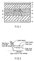
- FIG. 5 shows a sectional structure of a generally used buried-type semiconductor laser capable of obtaining a high efficiency laser light.
- the semiconductor laser of this type is conventionally known and disclosed in Jpn. Pat. Appln. No. 7-22691.
- a first clad layer 2 of a p-type InP is formed on a p-type InP substrate 1 having a (100) crystal plane or a crystal plane close to the (100) crystal plane as the upper surface.
- a mesa stripe portion 3 having a trapezoidal shape is formed on the upper center of the first clad layer 2.
- a current blocking portion 4 is formed outside the mesa stripe portion 3 on the first clad layer 2.
- the mesa stripe portion 3 is formed of a projecting portion 2a of the first clad layer 2, an active layer 5 of non-doped InGaAsP formed on the projecting portion 2a of the first clad layer 2, and a second clad layer 6 of n-type InP formed on the active layer 5.
- the current blocking portion 4 at both sides of the mesa stripe portion 3 is formed of an n-type current blocking layer 7 of n-type InP for blocking migration of holes present at the lower side, and a high resistance semiconductor layer 8 doped with Fe, for blocking migration of electrons present at the upper side.
- a third clad layer 9 of n-type InP is formed so as to simultaneously cover the upper surface of the mesa stripe portion 3 and the upper surface of the current blocking portion 4.
- a contact layer 10 is formed on the third clad layer 9.
- an insulating layer 11 is formed so as to face the current blocking portion 4.
- An electrode plate 12 is attached to the portion of the upper surface of the contact layer 10 facing to the mesa stripe portion 3.
- an electrode plate 13 is attached also on the lower surface of the P-type InP substrate 1.
- the current is concentrated on the mesa-stripe portion 3 at the center, increasing the efficiency of laser light emitting from the active layer 5 of the mesa stripe portion 3.
- a top-end 7a of the n-type current blocking layer 7 is positioned on the border between the active layer 5 and the second clad layer 6.
- etching is performed in its manufacturing process of the semiconductor laser in the conditions under which a (111)B crystal plane can be exposed on an inclined side surface 14 of the mesa stripe portion 3 having a trapezoidal shape.
- a (100) crystal plane is exposed by etching on the upper surface 15 of the first clad layer 2 outside the mesa stripe portion 3.
- the n-type current blocking layer 7 is grown on the inclined side surface 14 of the mesa stripe portion 3 and on the upper surface 15 of the first clad layer 2 by use of a metal-organic-vapor-phase epitaxy (MOVPE) method.
- MOVPE metal-organic-vapor-phase epitaxy
- the n-type current blocking layer 7 is grown directly on the (100) crystal plane but not grown directly on the (111)B crystal plane.
- n-type current blocking layer 7 is grown by use of the metal-organic-vapor-phase epitaxy (MOVPE) method, a tapered tip 7a of the n-type current blocking layer 7 creeps up along the inclined side surface 14 of the mesa stripe portion 3 in accordance with the growth of the n-type current blocking layer 7, as shown in FIG. 6.
- MOVPE metal-organic-vapor-phase epitaxy
- the tapered tip 7a of the n-type current blocking layer 7 reaches the border between the active layer 5 and the second clad layer 6, the growth operation of the n-type current blocking layer 7 by use of the metal-organic-vapor-phase epitaxy (MOVPE) method is terminated
- the manufacturing method mentioned above makes it possible to minimize the reactive current (leakage current) flowing from the second clad layer 6 to the n-type current blocking layer 7 without passing through the active layer 5 of the mesa stripe portion 3.
- the conventional semiconductor laser having the structure shown in FIG. 5 still have the following problems to be solved.
- the tapered tip 7a of the n-type current blocking layer 7 creeps up along the inclined side surface 14 of the mesa stripe portion 3 as it grows.
- the timing (time) at which the tapered tip 7a reaches the border between the active layer 5 and the second clad layer 6 varies depending upon voltage application conditions of the metal-organic-vapor-phase epitaxy (MOVPE) method and the height of the trapezoidal mesa stripe portion 3 which slightly varies depending upon etching conditions.
- MOVPE metal-organic-vapor-phase epitaxy
- the tapered tip 7a of the n-type current blocking layer 7 fails to reach the border between the active layer 5 and the second clad layer 6 in some cases, and in other cases, it reaches up to the middle of the side surface of the second clad layer 6.
- the first clad layer 2 (2a) of p-type InP may be brought into direct contact with the high resistance semiconductor layer 8.
- the amount of the reactive current (leakage current) flowing from the second clad layer 6 to the n-type current blocking layer 7 may increase, with the result that stable and high efficient laser-emitting characteristics as the semiconductor laser cannot be obtained.
- a p-type InP substrate is employed.
- the p-type InP substrate as is known well, has a high specific resistance compared to an n-type InP substrate.
- the semiconductor laser employing the p-type InP substrate is useful in the cases where a switching operation is carried out at a high speed, however is not suitable as a semiconductor laser like a light source for an optical communications system.
- Zn an impurity, Zn, diffuses within the p-type semiconductor more easily than within the n-type semiconductor. Therefore, when Zn is doped into a p-type InP substrate as an impurity, the diffusion of Zn is easily performed. It follows that Zn diffuses up to the area in the proximity of the active layer of the p-type InP first clad layer.
- the present invention is made in view of the aforementioned circumstances and an object of the present invention is to provide a semiconductor laser and a method of manufacturing the semiconductor laser which is formed by using an n-type semiconductor substrate and setting the inclination angle of the side surface of the mesa strip portion such that a (111)B crystal plane is not directly exposed in the inclined surface of the mesa stripe portion having a trapezoidal shape so as to control a reactive current not flowing through an active layer of the mesa stripe portion to fall within a predetermined range and to maintain a high withstand voltage at the current blocking portion, thereby attaining a high efficiency and high power laser light emission characteristics.
- a semiconductor laser comprising:
- the semiconductor laser according to the first aspect in which a thickness of the p-type current blocking layer in a direction perpendicular to an inclined side surface of the mesa stripe portion near the active layer is set to be thinner than a thickness in a direction perpendicular to the (100) crystal plane of the n-type semiconductor substrate; and an impurity concentration of the p-type current blocking layer near the active layer of the mesa stripe portion is set to be lower than an impurity concentration of the p-type current blocking layer near the (100) crystal plane of the n-type semiconductor substrate.
- the semiconductor laser according to the second aspect in which the n-type semiconductor substrate is formed of n-type InP; and the p-type current blocking layer is formed of p-type InP containing an impurity of Zn or Cd.
- the semiconductor laser according to any one of the first to third aspects, in which inclination of the side surface of the mesa stripe portion is set at an angle within (+1° to +5°) or (-1° to -5°) to the inclination angle of the (111)B crystal plane.
- a semiconductor laser according to any one of the first to fourth aspects, in which an upper end of the side surface of the mesa stripe portion is positioned higher than a vicinity of the active layer.
- a method of manufacturing a semiconductor laser comprising:
- the mesa stripe portion is formed by forming a mask on an upper surface of the second clad layer and etching the n-type first clad layer, the active layer, and the p-type second clad layer into a trapezoidal shape;
- the current blocking portion is formed by growing the p-type current blocking layer and the n-type current blocking layer on the side surface of the mesa stripe portion and on the upper surface of the n-type semiconductor substrate exposed by etching;
- the p-type third clad layer is formed so as to simultaneously cover both the upper surface of the mesa stripe portion from which the mask is removed and the upper surface of the current blocking portion;
- forming the mesa stripe portion comprises interposing a cap layer between the second clad layer and the mask; setting conditions of etching such that inclination of the side surface of the mesa stripe portion to be obtained by side etch
- the method of manufacturing a semiconductor laser according to the sixth aspect in which the n-type semiconductor substrate is InP doped with an n-type impurity, the first clad layer is InP doped with an n-type impurity, the active layer has a multiple quantum well structure consisting of non-doped InGaAs, non-doped InGaAsP, or a combination thereof, the second clad layer is InP doped with a p-type impurity, the cap layer is InGaAsP, and the p-type current blocking layer is p-type InP doped with an impurity of Zn or Cd.
- the present invention is applied to a semiconductor laser comprising an n-type semiconductor substrate; a mesa stripe portion having a trapezoidal shape, formed on the n-type semiconductor substrate, including an n-type first clad layer, an active layer, and a p-type second clad layer, and formed along a ⁇ 011> direction; a current blocking portion formed of a p-type current blocking layer formed on the n-type semiconductor substrate and outside the mesa stripe portion and an n-type current blocking layer formed on the p-type current blocking layer; and a p-type third clad layer simultaneously covering the upper surface of the mesa stripe portion and the upper surface of the current blocking portion.
- the n-type InP substrate has a (100) crystal plane as the upper surface.
- the inclination of the side surface of the mesa stripe portion having a trapezoidal shape and formed along the ⁇ 011> direction is set at an angle in the proximity of the specific angle at which a (111)B crystal plane is exposed but not set at the specific angle.
- the (111)B crystal plane is not exposed directly from the mesa stripe portion etched along the ⁇ 011> direction into a trapezoidal shape. Instead, a plane inclined at an angle near the inclination angle of the (111)B crystal plane is exposed.
- the (100) crystal plane of the n-type semiconductor substrate is exposed.
- the p-type current blocking layer forming the current block portion is grown at a predetermined rate which is determined by formation conditions such as time.
- the p-type current block layer is slightly grown. More specifically, the p-type current block layer grows at a slow rate which differs depending upon how the angle of the p-type current block layer differs from the inclination angle of the (111)B crystal plane.
- the p-type current blocking layer is grown almost uniformly over the side surface of the mesa stripe portion from the beginning of the growth.
- the reactive current flowing from the p-type second clad layer to the p-type current blocking layer can be minimized to a constant value without fail.
- the thickness of the p-type current blocking layer near the active layer in direction perpendicular to the inclined side surface of the mesa stripe portion is set to be thinner than the thickness in the direction perpendicular to the (100) crystal plane of the n-type semiconductor substrate.
- the impurity concentration of the p-type current blocking layer near the active layer, that is, near the mesa stripe portion is set to be lower than that near the (100) crystal plane of the n-type semiconductor substrate.
- the growth rate of the p-type current blocking layer near the (111)B crystal plane is considerably small to that near the (100) crystal plane.
- the amount of the impurity left inside namely, an impurity concentration, differs depending upon the relationship between the doping direction and the crystal plane.
- the concentration with respect to the direction of the (100) crystal plane of the n-type semiconductor substrate is larger than that with respect to the direction of the plane in the proximity of the (111)B crystal plane of the mesa stripe portion.
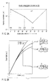
- FIG. 3A shows a characteristic graph of impurity concentration experimentally obtained. More specifically, FIG. 3A shows the relationship between the direction of the crystal plane (crystal-plane angle) and the impurity concentration when Zn is doped as an impurity into InP at a constant doping rate while gradually changing the direction (angle) of the crystal plane to be doped.
- a change amount in direction of each crystal plane from the (100) crystal plane is indicated in terms of an angle (°) based on the (100) crystal plane as being 0°.
- the concentration with respect to the direction of the (100) crystal plane is larger about ten times than that with respect to the direction of the (111) crystal plane.
- the fact that the impurity concentration of the p-type current blocking portion near the mesa stripe portion is low means that the electronic resistance of the p-type current blocking portion near the mesa stripe portion is high.
- the reactive current flowing through the p-type current blocking portion near the mesa stripe portion can be further reduced.
- the impurity concentration of the p-type current blocking layer near the (100) crystalline plane of the n-type semiconductor substrate is high, it becomes difficult to turn on (become conductive) a thyristor of a p-n-p-n structure formed of the p-type third clad layer, n-type current blocking layer, p-type current blocking layer, and n-type semiconductor substrate. It follows that a high voltage can be applied by the semiconductor laser, stabilizing the characteristics of the semiconductor laser.
- Still another invention provides the semiconductor laser mentioned above in which the n-type semiconductor substrate is formed of n-type.InP and the p-type current blocking layer is formed of a p-type InP doped with Zn or Cd as an impurity.
- the resistance of the n-type InP substrate can be reduced compared to the p-type InP substrate. Therefore, the use of the n-type InP substrate makes it possible to generate heat in a reduced amount even if a large amount of current is supplied to the semiconductor laser. For the reason, high-power laser light can be obtained simply by increasing the amount of current.
- the impurity within the p-type InP substrate diffuses toward the active layer in the course of the growth from the first clad layer ⁇ the active layer ⁇ the second clad layer ⁇ the blocking layer ⁇ the third clad layer.
- the n-type InP substrate is free from such a disadvantage.
- the inclination of the side wall of the mesa stripe portion (hereinafter sometimes referred as "mesa angle") in the semiconductor laser of the invention mentioned above is set at an angle within (+1° to +5°) or (-1° to -5°) to the specific angle at which the (111)B crystal plane is exposed.
- FIG. 3B is a characteristic graph showing current versus light emission for semiconductor layers different in mesa angle and in impurity concentration of the p-type blocking layer.
- a to C curves show characteristic changes when only mesa angle changes while a doping amount to the p-type blocking layer is maintained constant.
- the concentration of the impurity of the mesa side surface increases. Since the electric resistance thus decreases, the amount of the reactive current, which flows from the p-type second clad layer to the n-type semiconductor substrate through the p-type current blocking layer, increases. As is clear from the figure that the light emission is saturated earlier as the mesa angle increases.
- the impurity concentration of the p-type current blocking layer is set to be lower than that of the case of C by a factor of about 10.
- the electric resistance of the mesa side surface is high and the reactive current is low. Therefore, the saturation characteristic is improved in the middle.
- the impurity concentration of the p-type current blocking layer on the (100) crystal surface is uniformly reduced, the thyristor of a p-n-p-n structure formed of the p-type third clad layer, n-type current blocking layer, p-type current blocking layer, and n-type semiconductor substrate is turned on at a low current.
- Another invention is applied to a method of manufacturing a semiconductor laser, comprising: growing an n-type first clad layer, an active layer, and a p-type second clad layer sequentially on an n-type semiconductor substrate having a (100) crystal plane as the upper surface; forming a mask over the upper surface of the second clad layer thus grown and etching the structure including the n-type first clad layer, the active layer, and the p-type second clad layer into a trapezoidal shape, thereby forming a mesa stripe portion; growing a p-type current blocking layer and an n-type current blocking layer sequentially on sides of the mesa stripe portion thus formed and on the exposed upper surface of the n-type semiconductor substrate, thereby forming a current blocking portion; and removing the mask, and forming a p-type third clad layer which simultaneously covers the upper surface of the mesa stripe portion from which the mask is removed and the upper surface of the current blocking portion.
- a cap layer is formed between the second clad layer and the mask.
- the conditions of side-etching of the cap layer are set such that the inclination angle of a side surface of the mesa stripe portion falls within the proximity of a specific angle at which the (111)B crystal plane is exposed, excluding the specific angle.
- the block layer is formed using a metal-organic-vapor-phase epitaxy method.
- the cap layer is removed simultaneously with the mask.
- the cap layer is interposed between the p-type second clad layer and the mask, and the side surfaces of the mesa stripe portion are made closer to the (111)B crystal plane by setting the etching conditions appropriately.
- another invention is the method of manufacturing a semiconductor laser according to the invention mentioned above, in which the n-type semiconductor substrate is InP doped with an n-type impurity, the first clad layer is InP doped with an n-type impurity, the active layer has a multiple quantum well structure formed of non-doped InGaAs, non-doped InGaAsP, or a combination thereof, the second clad layer is InP doped with a p-type impurity, and the cap layer is InGaAsP. Furthermore, the p-type current blocking layer is formed of a p-type InP doped with an impurity, Zn or Cd. Also, an n-type current blocking layer is formed of a InP doped with an n-type impurity.
- FIG. 1 is a schematic sectional view showing a structure of a semiconductor laser according to an embodiment of the present invention.
- a mesa stripe portion 22 having a trapezoidal shape is formed at the center of the upper surface of an n-type InP substrate 21 formed of a semiconductor material, doped with an n-type impurity and having a (100) crystal plane as the upper surface.
- a current blocking portion 23 is formed outside the mesa stripe portion 22 formed on the n-type InP substrate 21.
- an n-type first clad layer 24 of 0.5 ⁇ m thick containing an n-type impurity in a concentration of 1.0 X 10 18 cm -3 is formed in contact with the n-type InP substrate 21.
- an active layer 25 of 0.2 ⁇ m thick is formed of a multi quantum well structure consisting of non-doped InGaAs, non-doped InGaAsP, or a combination thereof.
- a p-type second clad layer 26 of 0.45 ⁇ m thick which contains a p-type impurity in a concentration of 5-7 X 10 17 cm -3 .
- the inclination angle of a side surface 27 in contact with the current blocking portion 23 of the mesa stripe portion 22 is set at 54.7° ( ⁇ ) ⁇ 1° to 5° (minor angle ⁇ ⁇ ) where 54.7° is an angle at which the (111)B crystal plane is exposed.
- the minor angle of ⁇ ⁇ is set at ⁇ 1° to 5°.
- the current blocking portion 23 positioned at both sides of the mesa stripe portion 22 is formed of a p-type current blocking layer 29 of p-type InP (positioned at a lower side) and an n-type current blocking layer 30 of n-type InP (positioned at an upper side).
- the tip portion 35 of the p-type current blocking layer 29 (positioned at the lower side) is positioned higher than the upper surface of the mesa stripe portion 22.
- Zn or Cd is employed as the p-type impurity for the p-type current blocking layer 29.
- the impurity concentration thereof near the upper surface 28 of the n-type InP substrate 21 is higher than that in the proximity of the side surface 27 of the mesa stripe portion 22.
- Si is employed as the n-type impurity of the n-type current blocking layer 30 positioned at the upper side.
- the concentration of the n-type impurity of the n-type current blocking layer 30 is 2 X 10 18 cm -3 .
- a p-type third clad layer 31 of 2.5 ⁇ m thick containing 1.0 X 10 18 cm -3 of a p-type impurity is formed so as to commonly cover the upper surface of the mesa stripe portion 22 and the upper surface of the current blocking portion 23.
- a contact layer 32 of InGaAsP or InGaAs is formed on the third clad layer 31 .
- an electrode plate 33 is attached.
- an electrode plate 34 is attached on the lower surface of the n-type InP substrate 21.
- the inclination angle of the side surface 27 of the mesa stripe portion 22 in contact with the current blocking portion 23 is set at 54.7° ( ⁇ ) ⁇ 1° to 5° (minor angle ⁇ ⁇ ) where 54.7° is an angle at which the (111)B crystal plane is exposed.
- the impurity concentration near the n-type InP substrate 21 is set to be higher than that near the side surface 27 of the mesa stripe portion 22.
- the p-type current blocking layer 29 is formed almost uniformly over the side surface 27 of the mesa stripe portion 22 from the beginning of the growth.
- the reactive current flowing from the p-type second clad layer to the n-type InP substrate 21 by way of the p-type current blocking layer 29 can be minimized to a constant value without fail.
- the high-power laser light is obtained by increasing the amount of current.
- the n-type first clad layer 24 of 0.5 ⁇ m thick doped with an n-impurity of 1.0 X 10 18 cm -3 is formed by a metal-organic-vapor-phase epitaxy (MOVPE) method.
- MOVPE metal-organic-vapor-phase epitaxy
- the active layer 25 of a multiple quantum well structure formed of a non-doped InGaAs, a non-doped InGaAsP, or a combination thereof is formed with a thickness of 0.2 ⁇ m.
- the p-type second clad layer 26 doped with a p-type impurity of 5 to 7 X 10 17 cm -3 is formed with a thickness of 0.45 ⁇ m.
- the p-type cap layer 36 of p-type InGaAsP doped with a p-type impurity of 5-7 X 10 17 cm -3 is formed with a thickness of 0.15 ⁇ m.
- the mask 37 of SiNx is formed with a thickness of 80 nm by plasma CVD.
- the mask 37 formed on the cap layer 36 is then etched into stripes in the direction of a ⁇ 011> direction by use of a photolithographic technique.
- the width of the stripe is set to be slightly wider than the width of the upper surface of the trapezoidal mesa stripe portion 22 to be formed.
- the portion of the resultant structure except the mask 37 is selectively etched in the ⁇ 011> direction to obtain the trapezoidal mesa stripe portion 22 of 2.4 ⁇ m height, as shown in FIG. 4D.
- the etching rate of the cap layer 36 is faster than other portion(s), so that the etching speed for the portions under the cap layer increases.
- the side-etching amount of the cap layer 36 is controlled, it is possible to form the side surface 27 of the mesa stripe portion 22 inclined at a desired inclination angle.
- the inclination angle of the side surface 27 of the mesa stripe portion 22 can be set at 54.7° ( ⁇ ) ⁇ 1 to 5° (minor angle ⁇ ⁇ ) where 54.7° is an angle at which the (111)B crystal plane is exposed.
- the eaves 37a has a function of preventing the tip portion 35 of the p-type current blocking layer 29 from significantly protruding from the top end of the mesa stripe portion 22.
- the p-type current blocking layer 29 containing an impurity (Zn) in a concentration of 1 X 10 18 cm -3 is formed with a thickness of 0.7 ⁇ m by the aforementioned metal-organic-vapor-phase epitaxy (MOVPE) method.
- MOVPE metal-organic-vapor-phase epitaxy
- the n-type current blocking layer 30 containing an impurity (Si) in a concentration of 2 X 10 18 cm -3 is formed with a thickness of 1.15 ⁇ m by the aforementioned metal organic vapor phase epitaxy (MOVPE) method.
- MOVPE metal organic vapor phase epitaxy
- the current blocking portion 23 is formed of the p-type current blocking layer 29 and the n-type current blocking layer 30.
- the cap layer 36 and the mask 37 on the p-type second clad layer 26 of the mesa stripe portion 22 are removed with a solvent to expose the upper surface of the p-type second clad layer 26.
- the p-type third clad layer 31 containing a p-type impurity in a concentration of 1 X 10 18 cm -3 is formed with a thickness of 2.5 ⁇ m so as to simultaneously cover them.
- a contact layer 32 of InGaAsP or InGaAs is formed on the third clad layer 31 .
- the electrode plate 33 is attached to the upper surface of the contact layer 32.
- the electrode plate 34 is attached on the lower surface of the n-type InP substrate 21.
- the cap layer 36 is formed between the p-type second clad layer 26 and the mask 37 of the mesa stripe portion 22 and etching is performed under the aforementioned conditions.
- the side surface 27 of the mesa stripe portion 22 is formed so as to have a crystal plane close to the (111)B crystal plane but not equal to the (111)B crystal plane itself.
- the p-type current blocking layer 29 having the aforementioned two excellent characteristics on the side surface 27 of the mesa stripe portion 22 and on the upper surface 28 of the n-type InP substrate 21.
- the side surface of the mesa stripe portion having a trapezoidal shape is set so as to have a crystal plane which is close to the (111) crystal plane but not equal to the (111) crystal plane itself.
- the thickness of the p-type current blocking layer in contact with the side surface of the mesa stripe can be controlled to be constant and thin. Furthermore, the impurity concentration of the p-type current blocking layer near the active layer of the mesa stripe portion can be set to be lower than that near the (100) crystal plane of the n-type semiconductor substrate.
- the reactive current flowing the p-type current blocking layer can be controlled within a certain value and a high withstand voltage can be maintained in the current blocking portion.
- high-power laser light can be stably emitted with high efficiency.
- the specific resistance can be reduced.
- the high-power laser light can be readily obtained simply by increasing the current.
- the n-type semiconductor substrate is used.
- the inclination angle of the side surface of the mesa stripe portion is set so as not to directly expose the (111)B crystal plane. Therefore, the reactive current not flowing through the active layer of the mesa stripe portion can be controlled within a predetermined level. Furthermore, high withstand voltage of the current blocking portion can be maintained. Hence, it is possible to provide a semiconductor laser and a method of manufacturing the semiconductor laser capable of providing stable, high efficiency and high power light-emission characteristics.
Landscapes
- Physics & Mathematics (AREA)
- Geometry (AREA)
- Condensed Matter Physics & Semiconductors (AREA)
- General Physics & Mathematics (AREA)
- Electromagnetism (AREA)
- Optics & Photonics (AREA)
- Semiconductor Lasers (AREA)
- Weting (AREA)
Abstract
Description
an n-type current blocking layer is formed on the p-type current blocking layer; and
a thickness of the p-type current blocking layer in a direction perpendicular to an inclined side surface of the mesa stripe portion near the active layer is set to be thinner than a thickness in a direction perpendicular to the (100) crystal plane of the n-type semiconductor substrate; and
an impurity concentration of the p-type current blocking layer near the active layer of the mesa stripe portion is set to be lower than an impurity concentration of the p-type current blocking layer near the (100) crystal plane of the n-type semiconductor substrate.
the n-type semiconductor substrate is formed of n-type InP; and
the p-type current blocking layer is formed of p-type InP containing an impurity of Zn or Cd.
a p-type second clad layer;
in which the mesa stripe portion is formed by forming a mask on an upper surface of the second clad layer and etching the n-type first clad layer, the active layer, and the p-type second clad layer into a trapezoidal shape;
the current blocking portion is formed by growing the p-type current blocking layer and the n-type current blocking layer on the side surface of the mesa stripe portion and on the upper surface of the n-type semiconductor substrate exposed by etching;
the p-type third clad layer is formed so as to simultaneously cover both the upper surface of the mesa stripe portion from which the mask is removed and the upper surface of the current blocking portion;
forming the mesa stripe portion comprises
interposing a cap layer between the second clad layer and the mask;
setting conditions of etching such that inclination of the side surface of the mesa stripe portion to be obtained by side etching of the cap layer has an angle near a predetermined angle at which the (111)B crystal plane is exposed, excluding the predetermined angle; and
removing the mask simultaneously with the cap layer.
Claims (8)
- A semiconductor laser comprising:characterized in that an inclination angle being an acute angle of a side surface of said mesa stripe portion (22) having a trapezoidal shape and formed along a <011> direction is close to an inclination angle of a (111)B crystal plane with respect to the (100) crystal plane and set at one of an angle larger than and an angle smaller than the inclination angle of the (111)B crystal angle.an n-type semiconductor substrate (21) having a (100) crystal plane as an upper surface;a mesa stripe portion (22) having a trapezoidal shape and formed along a <011> direction, said mesa stripe portion (22) including an n-type first clad layer (24), an active layer (25), and a p-type second clad layer (26), which are successively formed on the n-type semiconductor substrate (21);a current blocking portion (23) formed of a p-type current blocking layer (29) formed outside the mesa stripe portion and on the n-type semiconductor substrate (21), and an n-type current blocking layer (30) is formed on the p-type current blocking layer (29); anda p-type third clad layer (31) simultaneously covering both the upper surface of the mesa stripe portion (22) and the upper surface of the current blocking portion (23),
- The semiconductor laser according to claim 1,
characterized in that
a thickness of said p-type current blocking (29) layer in a direction perpendicular to an inclined side surface of the mesa stripe portion (22) near the active layer (25) is set to be thinner than a thickness in a direction perpendicular to the (100) crystal plane of the n-type semiconductor substrate (21); and
an impurity concentration of said p-type current blocking layer (29) near the active layer (25) of the mesa stripe portion (22) is set to be lower than an impurity concentration of said p-type current blocking layer (29) near the (100) crystal plane of the n-type semiconductor substrate (21). - The semiconductor laser according to claim 2,
characterized in that
said n-type semiconductor substrate (21) is formed of n-type InP; and
said p-type current blocking layer (29) is formed of p-type InP containing an impurity of Zn or Cd. - The semiconductor laser according to any one of claims 1 to 3, characterized in that inclination of the side surface of the mesa stripe portion (22) is set at an angle within (+1° to +5°) or (-1° to -5°) to the inclination angle of the (111)B crystal plane.
- The semiconductor laser according to any one of claims 1 to 4, characterized in that an upper end of the side surface of the mesa stripe portion (22) is positioned higher than an vicinity of the active layer.
- A method of manufacturing a semiconductor laser comprising the steps of:characterized in that an inclination angle being an acute angle of the side surface of the mesa stripe portion (25) having a trapezoidal shape and formed along the <011> direction is close to an inclination angle of a (111)B crystal plane with respect to the (100) crystal plane and set at one of an angle larger than and an angle smaller than an inclination angle of the (111)B crystal plane.preparing an n-type semiconductor substrate (21) having a (100) crystal plane as an upper surface;stacking an n-type first clad layer (24), an active layer (25), and a p-type second clad layer (26) sequentially on the n-type semiconductor substrate (21), and, forming a mesa stripe portion (22) having a trapezoidal shape along a <011> direction, said mesa stripe portion (22) including the n-type first clad layer (24), the active layer (25), and a p-type second clad layer (26);forming an p-type current blocking layer (29) outside the mesa stripe portion (25) and on the n-type semiconductor substrate (21) and an n-type current blocking layer (30) on the p-type current blocking layer (29), as the current blocking portion (23) using a metal organic vapor phase epitaxy (MOVPE) method; andcovering both an upper surface of the mesa stripe portion (25) and an upper surface of the current blocking portion with a p-type third clad layer (31),
- The method according to claim 6,
characterized in that
said mesa stripe portion (22) is formed by forming a mask on an upper surface of the second clad layer (26) and etching the n-type first clad layer (24), the active layer (25), and the p-type second clad layer (26) into a trapezoidal shape;
said current blocking portion (23) is formed by growing the p-type current blocking layer (29) and the n-type current blocking layer (30) on the side surface of the mesa stripe portion (22) and on the upper surface of the n-type semiconductor substrate (21) exposed by etching;
said p-type third clad layer (31) is formed so as to simultaneously cover both the upper surface of the mesa stripe portion (22) from which the mask is removed and the upper surface of the current blocking portion (23);
the mesa stripe portion (22) comprises
interposing a cap layer between the second clad layer (26) and the mask;
setting conditions of etching performed such that inclination of the side surface of the mesa stripe portion (22) to be obtained by side etching of the cap layer has an angle near a predetermined angle at which the (111)B crystal plane is exposed, excluding the predetermined angle; and
removing the mask simultaneously with the cap layer. - The method according to claim 6, characterized in that said n-type semiconductor substrate (22) is InP doped with an n-type impurity, said first clad layer (24) is InP doped with an n-type impurity, said active layer (25) has a multiple quantum well structure consisting of non-doped InGaAs, non-doped InGaAsP, or a combination thereof, said second clad layer (26) is InP doped with a p-type impurity, said cap layer is InGaAsP, and the p-type current blocking layer (29) is p-type InP doped with an impurity of Zn or Cd.
Applications Claiming Priority (2)
| Application Number | Priority Date | Filing Date | Title |
|---|---|---|---|
| JP2001055109A JP3718129B2 (en) | 2001-02-28 | 2001-02-28 | Semiconductor laser and manufacturing method thereof |
| JP2001055109 | 2001-02-28 |
Publications (3)
| Publication Number | Publication Date |
|---|---|
| EP1237241A2 true EP1237241A2 (en) | 2002-09-04 |
| EP1237241A3 EP1237241A3 (en) | 2003-07-16 |
| EP1237241B1 EP1237241B1 (en) | 2005-04-27 |
Family
ID=18915342
Family Applications (1)
| Application Number | Title | Priority Date | Filing Date |
|---|---|---|---|
| EP02002704A Expired - Lifetime EP1237241B1 (en) | 2001-02-28 | 2002-02-06 | Semiconductor laser and method of manufacturing |
Country Status (4)
| Country | Link |
|---|---|
| US (1) | US6697407B2 (en) |
| EP (1) | EP1237241B1 (en) |
| JP (1) | JP3718129B2 (en) |
| DE (1) | DE60203840T2 (en) |
Families Citing this family (7)
| Publication number | Priority date | Publication date | Assignee | Title |
|---|---|---|---|---|
| JP3994928B2 (en) * | 2003-06-11 | 2007-10-24 | 住友電気工業株式会社 | Manufacturing method of semiconductor laser |
| US6892010B2 (en) * | 2003-09-09 | 2005-05-10 | Emcore Corporation | Photodetector/optical fiber apparatus with enhanced optical coupling efficiency and method for forming the same |
| JP5028640B2 (en) * | 2004-03-26 | 2012-09-19 | 日亜化学工業株式会社 | Nitride semiconductor laser device |
| JP2007049007A (en) * | 2005-08-11 | 2007-02-22 | Mitsubishi Electric Corp | Semiconductor laser device and manufacturing method thereof |
| JP5660940B2 (en) * | 2010-04-27 | 2015-01-28 | 住友電工デバイス・イノベーション株式会社 | Manufacturing method of optical semiconductor device |
| US20210313772A1 (en) * | 2018-11-01 | 2021-10-07 | Mitsubishi Electric Corporation | Optical semiconductor device and method for manufacturing optical semiconductor device |
| US12355210B1 (en) * | 2024-11-22 | 2025-07-08 | Hiefo Corporation | Semiconductor waveguide optical gain device with lateral current confinement |
Family Cites Families (7)
| Publication number | Priority date | Publication date | Assignee | Title |
|---|---|---|---|---|
| JP2827326B2 (en) | 1989-09-27 | 1998-11-25 | 住友電気工業株式会社 | Manufacturing method of semiconductor laser |
| US5260230A (en) | 1991-07-12 | 1993-11-09 | Nippon Telegraph And Telephone Corporation | Method of manufacturing buried heterostructure semiconductor laser |
| JP2823476B2 (en) * | 1992-05-14 | 1998-11-11 | 三菱電機株式会社 | Semiconductor laser and method of manufacturing the same |
| JPH0722691A (en) | 1993-06-30 | 1995-01-24 | Mitsubishi Electric Corp | Semiconductor laser and manufacturing method thereof |
| US5568501A (en) * | 1993-11-01 | 1996-10-22 | Matsushita Electric Industrial Co., Ltd. | Semiconductor laser and method for producing the same |
| JP3907854B2 (en) * | 1998-12-07 | 2007-04-18 | 富士通株式会社 | Semiconductor laser and manufacturing method thereof |
| JP2000244063A (en) * | 1999-02-19 | 2000-09-08 | Mitsubishi Electric Corp | Semiconductor laser device and method of manufacturing the same |
-
2001
- 2001-02-28 JP JP2001055109A patent/JP3718129B2/en not_active Expired - Lifetime
-
2002
- 2002-02-01 US US10/061,647 patent/US6697407B2/en not_active Expired - Lifetime
- 2002-02-06 DE DE60203840T patent/DE60203840T2/en not_active Expired - Lifetime
- 2002-02-06 EP EP02002704A patent/EP1237241B1/en not_active Expired - Lifetime
Also Published As
| Publication number | Publication date |
|---|---|
| EP1237241A3 (en) | 2003-07-16 |
| EP1237241B1 (en) | 2005-04-27 |
| US20020118717A1 (en) | 2002-08-29 |
| US6697407B2 (en) | 2004-02-24 |
| JP3718129B2 (en) | 2005-11-16 |
| DE60203840D1 (en) | 2005-06-02 |
| DE60203840T2 (en) | 2006-01-19 |
| JP2002261390A (en) | 2002-09-13 |
Similar Documents
| Publication | Publication Date | Title |
|---|---|---|
| JP2823476B2 (en) | Semiconductor laser and method of manufacturing the same | |
| US6320209B1 (en) | Epitaxial lateral overgrowth of gallium nitride based semiconductive oxide selective growth mask and method for fabricating the same | |
| US5452315A (en) | Semiconductor laser with semi-insulating current blocking layers | |
| EP0433051B1 (en) | A semiconductor laser device and a method of producing the same | |
| JP2595457B2 (en) | RWG type semiconductor laser device and manufacturing method | |
| CA2072632A1 (en) | Structure and method for fabricating indium phosphide/indium gallium arsenide phosphide buried heterostructure semiconductor lasers | |
| US6556605B1 (en) | Method and device for preventing zinc/iron interaction in a semiconductor laser | |
| EP1237241B1 (en) | Semiconductor laser and method of manufacturing | |
| EP0264225B1 (en) | A semiconductor laser device and a method for the production of the same | |
| US5748659A (en) | Semiconductor laser device | |
| EP0473443B1 (en) | Buried-stripe type semiconductor laser device | |
| US5149670A (en) | Method for producing semiconductor light emitting device | |
| US20080283852A1 (en) | Light-emitting device and a method for producing the same | |
| US5222091A (en) | Structure for indium phosphide/indium gallium arsenide phosphide buried heterostructure semiconductor | |
| US5887011A (en) | Semiconductor laser | |
| JPH07254750A (en) | Semiconductor laser | |
| JP2940158B2 (en) | Semiconductor laser device | |
| JP3652454B2 (en) | Semiconductor laser and manufacturing method thereof | |
| EP0867949B1 (en) | Semiconductor light-emitting device | |
| JPH07169993A (en) | Semiconductor structure and semiconductor light emitting device | |
| JP3994928B2 (en) | Manufacturing method of semiconductor laser | |
| JP2910120B2 (en) | Semiconductor laser | |
| JP3522151B2 (en) | Method for manufacturing compound semiconductor laser | |
| JP2547458B2 (en) | Semiconductor laser device and manufacturing method thereof | |
| JPH0810780B2 (en) | Method for manufacturing semiconductor laser |
Legal Events
| Date | Code | Title | Description |
|---|---|---|---|
| PUAI | Public reference made under article 153(3) epc to a published international application that has entered the european phase |
Free format text: ORIGINAL CODE: 0009012 |
|
| 17P | Request for examination filed |
Effective date: 20020206 |
|
| AK | Designated contracting states |
Kind code of ref document: A2 Designated state(s): AT BE CH CY DE DK ES FI FR GB GR IE IT LI LU MC NL PT SE TR |
|
| AX | Request for extension of the european patent |
Free format text: AL;LT;LV;MK;RO;SI |
|
| PUAL | Search report despatched |
Free format text: ORIGINAL CODE: 0009013 |
|
| AK | Designated contracting states |
Designated state(s): AT BE CH CY DE DK ES FI FR GB GR IE IT LI LU MC NL PT SE TR |
|
| AX | Request for extension of the european patent |
Extension state: AL LT LV MK RO SI |
|
| 17Q | First examination report despatched |
Effective date: 20031126 |
|
| AKX | Designation fees paid |
Designated state(s): DE FR GB IT |
|
| GRAP | Despatch of communication of intention to grant a patent |
Free format text: ORIGINAL CODE: EPIDOSNIGR1 |
|
| RIN1 | Information on inventor provided before grant (corrected) |
Inventor name: KIKUGAWA, TOMOYUKI Inventor name: NAGASHIMA, YASUAKI Inventor name: SHINONE, KATSUNORI |
|
| GRAS | Grant fee paid |
Free format text: ORIGINAL CODE: EPIDOSNIGR3 |
|
| GRAA | (expected) grant |
Free format text: ORIGINAL CODE: 0009210 |
|
| AK | Designated contracting states |
Kind code of ref document: B1 Designated state(s): DE FR GB IT |
|
| REG | Reference to a national code |
Ref country code: GB Ref legal event code: FG4D |
|
| REF | Corresponds to: |
Ref document number: 60203840 Country of ref document: DE Date of ref document: 20050602 Kind code of ref document: P |
|
| ET | Fr: translation filed | ||
| PLBE | No opposition filed within time limit |
Free format text: ORIGINAL CODE: 0009261 |
|
| STAA | Information on the status of an ep patent application or granted ep patent |
Free format text: STATUS: NO OPPOSITION FILED WITHIN TIME LIMIT |
|
| 26N | No opposition filed |
Effective date: 20060130 |
|
| REG | Reference to a national code |
Ref country code: FR Ref legal event code: PLFP Year of fee payment: 15 |
|
| REG | Reference to a national code |
Ref country code: FR Ref legal event code: PLFP Year of fee payment: 16 |
|
| REG | Reference to a national code |
Ref country code: FR Ref legal event code: PLFP Year of fee payment: 17 |
|
| PGFP | Annual fee paid to national office [announced via postgrant information from national office to epo] |
Ref country code: FR Payment date: 20210113 Year of fee payment: 20 |
|
| PGFP | Annual fee paid to national office [announced via postgrant information from national office to epo] |
Ref country code: DE Payment date: 20210126 Year of fee payment: 20 Ref country code: GB Payment date: 20210127 Year of fee payment: 20 |
|
| PGFP | Annual fee paid to national office [announced via postgrant information from national office to epo] |
Ref country code: IT Payment date: 20210112 Year of fee payment: 20 |
|
| REG | Reference to a national code |
Ref country code: GB Ref legal event code: PE20 Expiry date: 20220205 |
|
| PG25 | Lapsed in a contracting state [announced via postgrant information from national office to epo] |
Ref country code: GB Free format text: LAPSE BECAUSE OF EXPIRATION OF PROTECTION Effective date: 20220205 |