EP1237240A2 - Drive current supply circuit - Google Patents
Drive current supply circuit Download PDFInfo
- Publication number
- EP1237240A2 EP1237240A2 EP02251425A EP02251425A EP1237240A2 EP 1237240 A2 EP1237240 A2 EP 1237240A2 EP 02251425 A EP02251425 A EP 02251425A EP 02251425 A EP02251425 A EP 02251425A EP 1237240 A2 EP1237240 A2 EP 1237240A2
- Authority
- EP
- European Patent Office
- Prior art keywords
- circuit
- current
- component
- drive
- current mirror
- Prior art date
- Legal status (The legal status is an assumption and is not a legal conclusion. Google has not performed a legal analysis and makes no representation as to the accuracy of the status listed.)
- Withdrawn
Links
Images


Classifications
-
- H—ELECTRICITY
- H01—ELECTRIC ELEMENTS
- H01S—DEVICES USING THE PROCESS OF LIGHT AMPLIFICATION BY STIMULATED EMISSION OF RADIATION [LASER] TO AMPLIFY OR GENERATE LIGHT; DEVICES USING STIMULATED EMISSION OF ELECTROMAGNETIC RADIATION IN WAVE RANGES OTHER THAN OPTICAL
- H01S5/00—Semiconductor lasers
- H01S5/04—Processes or apparatus for excitation, e.g. pumping, e.g. by electron beams
- H01S5/042—Electrical excitation ; Circuits therefor
Definitions
- the present invention relates to a drive current supply circuit.
- Drive current supply circuits have been developed for laser diodes in optical pickups.
- Prior art drive current supply circuits are disclosed in published Japanese Patent No. H. 7-31823 and US Patent No. 5898334.
- the drive current to the laser diode in an optical pickup is different during writing to the storage medium and during reading, being set to a larger value during writing.
- the drive current supply circuits described above are effective when the drive current is to be made variable.
- an object of the present invention is to provide a drive current supply circuit wherein the speed of rise of the drive current to the laser diode constituting the load can be increased.
- the DC component is applied to the line when reading data from an optical disk such as CD-R, CD-RW, DVD-R or DVD-RW
- the drive signal component is applied to the line when writing data on the optical disk.
- the drive signal component may be a signal modulated by using eight to fourteen modulation (EFM).
- EFM eight to fourteen modulation
- the DC and drive signal component may be modulated by high frequency.
- a current mirror circuit comprises two transistors and has two parallel lines.
- the current flowing through one line is equal to or proportional to the current flowing through the other line. Consequently, if the current flowing through the other line is controlled, the current flowing through the load connected to the one line can be controlled. This control is performed in accordance with a first control signal.
- a transistor has a threshold voltage at which current starts to flow. When voltage of above this threshold is applied between the control terminals of the transistor i.e. between the base/emitter in the case of a bipolar transistor or between the source/gate in the case of a field-effect transistor, current flows in the transistor and current therefore flows in the load.
- this first control signal consists solely of a DC component during reading and consists solely of an AC component during writing. Consequently, in the control circuit, the conventional AC signal during writing constitutes the drive signal and when the current flowing through the other line is controlled in accordance with the magnitude of this, the voltage between the control terminals starts to rise from 0 V and so can only reach the desired voltage level after passing through this threshold voltage.
- the first control signal comprises a steady DC component and a drive signal component added to this DC component when desired i.e. during writing
- the voltage between the control terminals has already reached a certain level, due to this DC component, so the amount of variation for this to reach the drive signal component is smaller, so the rise time is shorter.
- this DC component For the sake of this DC component, the level to which the voltage between the control terminals is to be raised can be determined as required.
- this drive current supply circuit When this drive current supply circuit is employed in reading and writing by an optical pickup, during reading, it sets the DC component at or above the threshold voltage of the transistor and during writing a drive signal component increment is superimposed on this, so a voltage of at or above the threshold voltage of the transistor is of course set between the control terminals and, when writing, a large drive current flows to the load i.e. the laser diode through one of the parallel lines in the current mirror circuit.
- steady means a continuous period in which there is no change whether in the reading period or in the writing period; it does not mean that the DC component does not change when the power source of the drive current supply circuit itself is OFF or when other control is being performed.
- this drive current supply circuit can be utilized in an optical pickup.
- the current mirror circuits could also be constructed of bipolar transistors, but, from the point of view of reducing power consumption, preferably consist of field-effect transistors.
- the first current mirror circuit may comprise two field-effect transistors with their gates connected in common, one channel of the field-effect transistors being the one of the lines, the other channel of the field-effect transistors being the other of the lines, the DC voltage applied to the gate being the DC component of the first control signal and the drive voltage applied to the gate being the drive signal component of the first control signal.
- the current flowing in the other line of the current mirror circuit changes depending on this first control signal. Since, as described above, the first control signal is set such that the rise during writing is speeded up, the rise of the drive current supplied to the load is speeded up.
- the drive current supply circuit in this case may further comprise at least a second current mirror circuit having two parallel lines, the one of the lines of the second current mirror circuit being connected with the load and wherein the control circuit controls the current flowing through the other of the lines of the second current mirror circuit in accordance with a second control signal, the second control signal comprising a steady DC component and, when desired, a drive signal component added to this DC component.
- a drive current supply circuit according to an embodiment is described below. Identical elements are given the same reference symbols to avoid duplicated description.
- Figure 1A is a circuit diagram of a drive current supply circuit according to an embodiment and Figure 1B is a circuit diagram of one of control circuits 11 to 41 shown in Figure 1A.
- this drive current supply circuit comprises a control circuit CONT that controls the current i flowing in an other-side one (1L) of the lines, in accordance with a first control signal ⁇ 1.
- the load 50 is a laser diode.
- This first control signal ⁇ 1 consists of a steady DC component ⁇ D and a drive signal component ⁇ 1 obtained by adding the increment ⁇ 1 of the drive signal component to the DC component ⁇ D when desired. It should be noted that "adding" is not restricted to addition of physical quantities which are both of positive sign.
- This first control signal ⁇ 1 is the potential of the gate of current mirror circuit 1.
- the DC component ⁇ D is applied to the line via resistance R1 when reading data from an optical disk such as CD-R, CD-RW, DVD-R or DVD-RW, and the drive signal component ⁇ 1 is applied to the line during writing data to the optical disk.
- the drive signal component may be a signal modulated by using eight to fourteen modulation (EFM).
- EFM eight to fourteen modulation
- the DC signal component and drive signal component may be modulated by high frequency.
- DVD requires 650 nm wavelength laser light for reading data
- CD requires 780 nm wavelength laser light for reading data. So, if the load 50, laser diode is applied to DVD/CD compatible player, the laser diode is comprised of two laser diodes, the respective diodes emitting 650 nm and 780 nm wavelength laser light, respectively.
- Current mirror circuit 1 comprises two transistors 1QR, 1QL and is provided with two parallel lines 1R, 1L.
- the current flowing through one-side line 1R is equal to or proportional to the current flowing through the other-side line 1L. Consequently, by controlling the current flowing through the other-side line 1L, the current flowing through the load 50 connected with the one-side line 1R can be controlled. This control is performed in accordance with the first control signal ⁇ 1.
- the current i 1 flowing in line 1L of first current mirror circuit 1 is determined by the DC component ⁇ D supplied from common partial control circuit 11 within control circuit CONT and the drive signal component ⁇ 1 supplied from first partial circuit 21.
- the first control signal ⁇ 1 becomes drive signal component ⁇ 1 as a result of addition of drive signal component increment ⁇ 1 (negative) to the DC component ⁇ D
- the first control signal ⁇ 1 becomes small, but since, in this example, we are considering the potential difference from this source to the gate of a transistor of high potential, the voltage obtained by subtracting first control signal ⁇ 1 from the source potential becomes large, so current i 1 is increased.
- the currents i 2 and i 3 flowing in the lines 2L and 3L of the second and third current mirror circuits 2, 3 are determined by the DC component ⁇ D supplied from the common partial control circuit 11 within control circuit CONT and the drive signal components ⁇ 2, ⁇ 3 supplied from the second and third partial circuits 31, 41. The operation is the same as in the case of the first current mirror circuit 1.
- the drive current supply circuit of this example is further provided with a second current mirror circuit 2 having at least two parallel lines, the one-side line 2R of the lines of this second current mirror circuit 2 being connected with a load 50; control circuit CONT controls the current flowing through the other-side line (2L) of the lines of second current mirror circuit 2 in accordance with a second control signal ⁇ 2; this second control signal ⁇ 2 consists of a steady DC component ⁇ D and a drive signal component ⁇ 2 that is added to this DC component when desired.
- control circuit CONT controls the current i3 flowing through the other-side line (3L) of the lines of third current mirror circuit 3 in accordance with a third control signal ⁇ 3;
- this third control signal ⁇ 3 consists of a steady DC component ⁇ D and a drive signal component ⁇ 3 that is added to this DC component when desired.
- first partial control circuit 21, second partial control circuit 31 and third partial control circuit 41 are function conversion circuits respectively comprising input terminals (12, 22, 32, 42), control input terminals (13, 23, 33, 43) and output terminals (terminals that supply ⁇ D, ⁇ 1, ⁇ 2 and ⁇ 3).
- the outputs supply ⁇ D, ⁇ 1, ⁇ 2 and ⁇ 3 are expressed by functions of the input to input terminals 12, 22, 32, 43, suitably by a proportionality relationship function.
- Control inputs 13, 23, 33, 43 input signals that control ON/OFF of the outputs ⁇ D, ⁇ 1, ⁇ 2 and ⁇ 3.
- Current mirror circuit 1 is provided with transistors 1QR, 1QL and lines 1R, 1L and is supplied with DC component ⁇ D and drive signal component ⁇ 1 and current i 1 flows in the lines 1L and 1R.
- current mirror circuit 2 replacing the 1 of the symbols used in current mirror circuit 1 by 2, there are provided transistors 2QR, 2QL and lines 2R, 2L and it is supplied with DC component ⁇ D and drive signal component ⁇ 2 and current i 2 flows in the lines 2L and 2R.
- transistors 3QR, 3QL and lines 3R, 3L are provided in current mirror circuit 3, replacing the 1 of the symbols used in current mirror circuit 1 by 3, and transistors 3QR, 3QL and lines 3R, 3L and it is supplied with DC component ⁇ D and drive signal component ⁇ 3 and current i 3 flows in the lines 3L and 3R.
- Transistors 1QR and 1QL in first current mirror circuit 1 are p-channel field-effect transistors, their sources being connected with +V volt power source potentials 25, 26 and their gates being connected in common. The gate and drain of transistor 1QL are short-circuited so that the gate voltage is controlled by the potential applied to the drain. In the case of p-channel field-effect transistors, the transistor is in ON condition when the voltage between the gate and source is set such that the gate potential is relatively negative with respect to the source.
- the current i 1 (drive current I) is controlled in accordance with the first control signal ⁇ 1 but, in this example, more precisely, the current i 1 is controlled in accordance with the voltage obtained by subtracting the gate (drain) potential ⁇ 1 from the source potential (+V) in transistor 1QL.
- Transistors 1QR and 1QL have a threshold voltage at which current starts to flow. This threshold value is set by the voltage between the gate and source in transistor 1QL i.e. by the drain/source voltage.
- transistor 1QL When greater voltage than or equal to the threshold voltage of transistor 1QL (
- Current mirror circuit 1 may be constituted of bipolar transistors but, with a view to reducing power consumption, is preferably constituted of field-effect transistors. However, if these transistors are bipolar transistors, the source, gate and drain referred to in the context of field-effect transistors may be respectively substituted by emitter, base and collector and in this case the voltage between the aforementioned control terminals therefore becomes the voltage between base and emitter.
- the load 50 in this example is a laser diode; this is employed in an optical pickup for reading from a storage medium and writing.
- Figure 1C is a circuit diagram of an optical disk player.
- the input data for writing is encoded by an encoder PL1 such as EFM circuit.
- the encoded data is applied to for example the control terminal 23 of the drive current supply circuit PL2 shown in Fig. 1A while applying DC voltage to the terminal 13.
- the load 50, laser diode emits laser light in response to the encoded data.
- a recording layer of the optical disk OPD changes its physical structure and the data is recorded in the optical disk OPD.
- the reflected laser light beam by the optical disk OPD is detected by a photodiode PL3.
- the electric output from the photodiode PL3 is inputted into a data regenerative circuit PL4 and the recorded data is extracted.
- the electric output is also applied to an auto power control (APC) circuit PL5 that controls the power applied to the laser diode 50.
- the APC circuit PL5 is controlled by a control circuit PL6. Note that such an APC control is used during writing, too.
- the control circuit PL6 also controls a spindle motor SM for rotating the optical disk OPD and a linear motor LM for moving the optical pick-up unit OPU including laser diode 50.
- the electrical output from the photodiode PL3 may be used for focusing the laser light beam. This focusing technique is conventional.
- the control circuit PL6 decides the laser power by the required physical status of the recording layer when the optical disk is CD-RW. For example, a middle power heating by laser light beam and gradual cooling causes the recording layer to become a crystalline. High power heating and rapid cooling causes the recording layer to become amorphous.
- the control circuit PL6 may decide the laser power by the kind of the optical disk OPD because the required laser power differs by the kind of the optical disk.
- the first control signal ⁇ 1 consists of a steady DC component ⁇ D and a drive signal component ⁇ 1 added to this DC component ⁇ D when desired i.e. when writing, from the standpoint of the source, the voltage across the control terminals has already reached a certain negative level because of this DC component ⁇ D, so, when drive signal component ⁇ 1 is generated by addition of the drive signal component increment ⁇ 1 thereto, its rise time in the negative direction is shortened.
- the potential of the DC component ⁇ D is lower than +V
- the potential of the drive current component ⁇ 1 is lower than the DC component ⁇ D.
- the DC component ⁇ D is chosen to be 4 V, and the center of amplitude of the drive signal component ⁇ 1 constituting the pulse signal is set at 2.5 V.
- ⁇ 1 in order to cause a current i 1 ' as shown in Figure 2, to be described, to pass, ⁇ 1 must be lowered from 5 V to 2.5 V; thus, regarding the difference of these as the gate/source voltage, from the standpoint of the source, a voltage of -2.5 V must be applied to the gate.
- a potential of for example 4 V is applied beforehand to the gate as ⁇ D, from the standpoint of the source, a voltage of -2.5 V can be applied to the gate simply by lowering ⁇ 1 from 4 V to 2.5 V. Since stray capacitance is of course present between the gate and source of the transistor, when the voltage between the gate and source is changed, some time is required for charging/discharging of this capacitance. Therefore, an excellent response characteristic of the output current can be obtained by making the change of the voltage between the gate and source small.
- a resistance R1 is inserted on a line connecting the line that supplies ⁇ 1 and the line that supplies ⁇ D, this resistance could be inserted in partial control circuit 11.
- the level to which the voltage between the control terminals should be raised is determined as needed by DC component ⁇ D.
- This drive current supply circuit when employed for reading and writing by an optical pickup, in the case of reading, sets DC component ⁇ D of at or above the threshold voltage of transistor 1QL so that normally drive current I flows; in the case of writing, it adds an increment thereto, replacing it with drive signal component ⁇ 1; thus a voltage of at or above the threshold voltage of transistor 1QL is of course set between the control terminals, so that, in the case of writing, a large current flows to load 50 i.e. the laser diode through one side of the parallel lines in the current mirror circuit 1.
- this threshold voltage is set lower than the voltage that applies a threshold value of drive current I that produces oscillation of laser diode (50).
- steady means a continuous period in which there is no change whether in the reading period or in the writing period; it does not mean that the DC component does not change when the power source of the drive current supply circuit itself is OFF or when other control is being performed.
- this drive current supply circuit can be utilized in an optical pickup when the load 50 is a laser diode.
- first current mirror circuit 1 comprises two field-effect transistors 1QR, 1QL with their gates connected in common, the one-side channel of the field-effect transistors being designated as the one-side line (1R), the other-side channel of the field-effect transistors being designated as the other-side line (1L), the DC voltage ⁇ D that is applied to the gate being designated as the DC component of the first control signal, and the drive voltage ⁇ 1 that is applied to the gate being designated as the drive signal of the first control signal.
- Control circuit CONT applies the DC voltage and the drive voltage to the gate.
- DC component ⁇ D is supplied from common partial control circuit 11 to each of the lines 1L, 2L, 3L and, if required, resistances R1, R2, R3 may be inserted as shown in the Figure on each line.
- a node 51 is formed by connection of all of 1R, 2R, 3R on one side of the parallel lines of the respective current mirror circuits 1, 2, 3.
- Load 50 is connected to node 51, so the currents i 1 , i 2 , i 3 flowing through the other sides 1L, 2L, 3L of the parallel lines of each of the current mirror circuits 1, 2, 3 are added i.e. the currents i 1 , i 2 , i 3 flowing through the one-side lines 1R, 2R, 3R are added and supplied to load 50 as drive current I.
- control signals supplied to the specified lines in a single current mirror circuit consisted solely of a DC component in the case of reading and consisted solely of an AC component modulated by the write information in the case of writing.
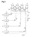
- FIG. 2 is a circuit diagram of a case in which this prior art circuit is somewhat improved.
- This circuit employs a plurality of current mirror circuits 1, 2, 3, D; current mirror circuit D that is supplied solely with DC component ⁇ D when reading is performed and current mirror circuits 1, 2, 3 that are supplied solely with AC components modulated by the write information when writing is performed are independently provided; drive current I to load 50 is constituted by adding the output currents i 1 ', i 2 ', i 3 ', i D ' of these current mirror circuits 1, 2, 3, D.
- control circuit CONT' controls the current i 1 ' flowing through the parallel lines of a specified current mirror circuit 1 in accordance with drive signal component ⁇ 1 consisting solely of an AC signal during performance of writing, directing attention to the specified current mirror circuit 1 that is supplied with this drive signal component, from the point of view of the source, the voltage between the control terminals (gate and source) starts to rise in the negative direction from 0 V and, exceeding this threshold voltage, attains a desired voltage level. Consequently, in comparison with the embodiment described above, the speed of rise in a circuit constructed as above is slow.
- Figure 3 is a graph showing the relationship between the gate/source voltage (gate voltage) and the drain current in a field-effect transistor.
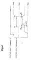
- Figure 4 is a timing chart in the circuit of Figure 2.
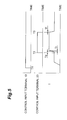
- Figure 5 is a timing chart in the circuit of Figure 1A.
- the timing of writing can be such that this is performed continuously with the condition in which the disc was being read.
- the optical disc is rotating, a condition is thereby produced in which the current for generating the laser beam for reading is always flowing.
- a condition in which control input terminal 13 is placed beforehand in ON condition so that a steady DC drive current I flows is often employed in actual optical pickups.
- the response characteristic of the laser beam is important; if the drive current supply circuit of the embodiment described above is employed, rise of the laser diode constituting load 50 can be achieved rapidly, so, in an optical pickup in which reading and writing are performed frequently, the writing speed can be increased.
- the speed of rise of the drive current to the laser diode constituting the load can be increased.
Landscapes
- Physics & Mathematics (AREA)
- Condensed Matter Physics & Semiconductors (AREA)
- General Physics & Mathematics (AREA)
- Electromagnetism (AREA)
- Optics & Photonics (AREA)
- Optical Head (AREA)
- Semiconductor Lasers (AREA)
- Control Of Electrical Variables (AREA)
Abstract
Description
Claims (4)
- A drive current supply circuit for supplying drive current to a laser diode used for reading data from and writing data on an optical disk, comprising:a first current mirror circuit having two parallel lines, said laser diode being connected with one of the two parallel lines; anda control circuit connected with the other of the two parallel lines, said control circuit controls the current flowing in this line in accordance with a potential of this line,this potential comprising a steady DC component when reading data; andthis potential comprising a drive signal component added to said DC component when writing data.
- The drive current supply circuit according to claim 1,
wherein said first current mirror circuit comprises first and second field-effect transistors with their gates connected in common,
wherein the channel of said first field-effect transistors is said one of said lines,
wherein the channel of said second field-effect transistors is said other of said lines. - The drive current supply circuit according to claim 1, further comprising a second current mirror circuit having two parallel lines, one of said lines of said second current mirror circuit being connected with said laser diode, and wherein said control circuit controls the current flowing through the other of said lines of said second current mirror circuit in accordance with a potential of the other of said lines,
this potential comprising a steady DC component when reading data; and
this potential comprising a drive signal component added to said DC component when writing data. - A drive circuit for supplying a load comprising a current supply circuit having a line driving said load, and a control circuit which applies a steady DC component to the line, and adds a varying drive signal to the DC when required.
Applications Claiming Priority (2)
| Application Number | Priority Date | Filing Date | Title |
|---|---|---|---|
| JP2001055929A JP2002261381A (en) | 2001-02-28 | 2001-02-28 | Drive current supply circuit |
| JP2001055929 | 2001-02-28 |
Publications (2)
| Publication Number | Publication Date |
|---|---|
| EP1237240A2 true EP1237240A2 (en) | 2002-09-04 |
| EP1237240A3 EP1237240A3 (en) | 2005-02-09 |
Family
ID=18916041
Family Applications (1)
| Application Number | Title | Priority Date | Filing Date |
|---|---|---|---|
| EP02251425A Withdrawn EP1237240A3 (en) | 2001-02-28 | 2002-02-28 | Drive current supply circuit |
Country Status (3)
| Country | Link |
|---|---|
| US (1) | US7046612B2 (en) |
| EP (1) | EP1237240A3 (en) |
| JP (1) | JP2002261381A (en) |
Cited By (1)
| Publication number | Priority date | Publication date | Assignee | Title |
|---|---|---|---|---|
| US11482836B2 (en) | 2020-01-28 | 2022-10-25 | Stmicroelectronics (Grenoble 2) Sas | Laser diode driver circuits and methods of operating thereof |
Families Citing this family (6)
| Publication number | Priority date | Publication date | Assignee | Title |
|---|---|---|---|---|
| US6912698B1 (en) * | 2002-05-23 | 2005-06-28 | Xilinx, Inc. | Skew lots for IC oscillators and other analog circuits |
| US7272159B1 (en) * | 2004-12-08 | 2007-09-18 | National Semiconductor Corporation | Apparatus and method for a laserdiode driver with a distributed current mirror |
| KR20080080382A (en) * | 2005-12-21 | 2008-09-03 | 코닌클리케 필립스 일렉트로닉스 엔.브이. | Multi-beam optical scanning device and method for measuring laser power of forward multiple laser beam |
| JP2010516012A (en) * | 2007-01-05 | 2010-05-13 | シリコン・コア・テクノロジー・インコーポレーテッド | High performance DVD write current circuit |
| CN108983860B (en) * | 2018-09-18 | 2024-01-12 | 杭州洪芯微电子科技有限公司 | Current self-checking regulating circuit based on voltage calibration |
| WO2020129238A1 (en) * | 2018-12-21 | 2020-06-25 | リコー電子デバイス株式会社 | Laser drive device |
Family Cites Families (19)
| Publication number | Priority date | Publication date | Assignee | Title |
|---|---|---|---|---|
| US4706252A (en) * | 1985-08-14 | 1987-11-10 | Kabushiki Kaisha Komatsu Seisakusho | Laser device of AC discharge excitation type |
| US4819241A (en) | 1985-08-16 | 1989-04-04 | Kabushiki Kaisha Toshiba | Laser diode driving circuit |
| IT1186424B (en) * | 1985-12-10 | 1987-11-26 | Gte Telecom Spa | SEMICONDUCTOR LASER MODULATOR |
| DE68921020T2 (en) | 1988-05-20 | 1995-06-29 | Mitsubishi Electric Corp | Integrated MOS circuit for controlling light-emitting diodes. |
| JP3031419B2 (en) * | 1990-06-13 | 2000-04-10 | 三菱電機株式会社 | Semiconductor integrated circuit |
| JP2550447B2 (en) * | 1991-05-16 | 1996-11-06 | 富士通株式会社 | Laser diode control method |
| JP2919233B2 (en) | 1993-07-19 | 1999-07-12 | 株式会社加藤厨房設備 | Oil smoke removal equipment for kitchen |
| JP3407827B2 (en) * | 1994-06-24 | 2003-05-19 | ローム株式会社 | Photodiode drive circuit |
| US5438581A (en) * | 1994-08-16 | 1995-08-01 | Eastman Kodak Company | Laser driver ASIC chip |
| JP3546521B2 (en) * | 1995-03-04 | 2004-07-28 | ソニー株式会社 | Laser light output control circuit |
| JP2999684B2 (en) * | 1995-03-10 | 2000-01-17 | 株式会社日立製作所 | Optical disk recording control method and optical disk device |
| JPH09116220A (en) * | 1995-10-20 | 1997-05-02 | Olympus Optical Co Ltd | Semiconductor laser control circuit |
| JP3266177B2 (en) | 1996-09-04 | 2002-03-18 | 住友電気工業株式会社 | Current mirror circuit, reference voltage generating circuit and light emitting element driving circuit using the same |
| US5898334A (en) | 1997-05-12 | 1999-04-27 | Elantec Semiconductor, Inc. | Reduced output capacitance circuit for driving a grounded load in response to a stepped input |
| JPH11126935A (en) * | 1997-10-23 | 1999-05-11 | Nippon Telegr & Teleph Corp <Ntt> | Laser diode drive circuit |
| JPH11225435A (en) * | 1997-11-10 | 1999-08-17 | Siliconix Inc | Method and circuit for operating infrared light emitting diode |
| US6496525B1 (en) * | 1998-09-21 | 2002-12-17 | Matsushita Electric Industrial Co., Ltd. | Laser driver and optical transceiver |
| US6516015B1 (en) * | 1998-11-19 | 2003-02-04 | Matsushita Electric Industrial Co., Ltd. | Laser driver and optical transceiver |
| DE10065838C2 (en) * | 2000-12-29 | 2003-06-26 | Infineon Technologies Ag | Electronic driver circuit for a directly modulated semiconductor laser |
-
2001
- 2001-02-28 JP JP2001055929A patent/JP2002261381A/en active Pending
-
2002
- 2002-02-28 US US10/084,341 patent/US7046612B2/en not_active Expired - Fee Related
- 2002-02-28 EP EP02251425A patent/EP1237240A3/en not_active Withdrawn
Cited By (2)
| Publication number | Priority date | Publication date | Assignee | Title |
|---|---|---|---|---|
| US11482836B2 (en) | 2020-01-28 | 2022-10-25 | Stmicroelectronics (Grenoble 2) Sas | Laser diode driver circuits and methods of operating thereof |
| US12388233B2 (en) | 2020-01-28 | 2025-08-12 | Stmicroelectronics (Grenoble 2) Sas | Laser diode driver circuits and methods of operating thereof |
Also Published As
| Publication number | Publication date |
|---|---|
| US7046612B2 (en) | 2006-05-16 |
| JP2002261381A (en) | 2002-09-13 |
| US20020118629A1 (en) | 2002-08-29 |
| EP1237240A3 (en) | 2005-02-09 |
Similar Documents
| Publication | Publication Date | Title |
|---|---|---|
| KR100800270B1 (en) | Laser power control device, optical head, recording device, and playback device | |
| JP2005191036A (en) | Light emitting element driving circuit, digital-analog converter, and current driving circuit | |
| KR20090124922A (en) | Thermal assist magnetic logger and thermal assist magnetic memory | |
| US7046612B2 (en) | Drive current supply circuit with current mirror | |
| KR920010019B1 (en) | Semiconductor laser driver | |
| US4718068A (en) | Stabilized laser device of optical information recording/reproduction apparatus | |
| US5586091A (en) | Magnetooptical recording apparatus including a control circuit for driving a switch element between on and off states in accordance with an error detection | |
| KR100517685B1 (en) | Semiconductor laser driving circuit and semiconductor laser driving method therefor | |
| US4967417A (en) | Laser driving device provided with two reference signal sources, and optical information recording apparatus using the same device | |
| US6563274B2 (en) | Light-emitting element drive circuit | |
| KR100894285B1 (en) | Semiconductor laser light output control circuit and optical device | |
| JPS60239929A (en) | optical recording and reproducing device | |
| JPH06139607A (en) | Laser diode drive circuit | |
| JP3898209B2 (en) | Optical information recording system | |
| JP3440497B2 (en) | Laser diode drive circuit | |
| JP4082030B2 (en) | Semiconductor laser drive circuit | |
| US7796659B2 (en) | Pickup head circuits | |
| JP3856804B2 (en) | Optical recording device | |
| KR100765734B1 (en) | Automatic Laser Diode Power Control in Laser Diode Driver | |
| JPH07129988A (en) | Semiconductor laser drive circuit | |
| JPH07307033A (en) | Semiconductor laser driving circuit for optical recorder | |
| JPH06267101A (en) | Semiconductor laser device and information recording and reproducing device | |
| KR20070027936A (en) | Laser diode driving circuit and its control method and semiconductor integrated circuit for driving laser diode | |
| US20050213468A1 (en) | Method and device for optical recording and optical record carrier | |
| JPH07129957A (en) | Laser drive circuit |
Legal Events
| Date | Code | Title | Description |
|---|---|---|---|
| PUAI | Public reference made under article 153(3) epc to a published international application that has entered the european phase |
Free format text: ORIGINAL CODE: 0009012 |
|
| AK | Designated contracting states |
Kind code of ref document: A2 Designated state(s): AT BE CH CY DE DK ES FI FR GB GR IE IT LI LU MC NL PT SE TR |
|
| AX | Request for extension of the european patent |
Free format text: AL;LT;LV;MK;RO;SI |
|
| PUAL | Search report despatched |
Free format text: ORIGINAL CODE: 0009013 |
|
| AK | Designated contracting states |
Kind code of ref document: A3 Designated state(s): AT BE CH CY DE DK ES FI FR GB GR IE IT LI LU MC NL PT SE TR |
|
| AX | Request for extension of the european patent |
Extension state: AL LT LV MK RO SI |
|
| RIC1 | Information provided on ipc code assigned before grant |
Ipc: 7G 11B 7/125 B Ipc: 7G 05F 3/26 B Ipc: 7H 01S 5/042 A |
|
| 17P | Request for examination filed |
Effective date: 20050726 |
|
| AKX | Designation fees paid |
Designated state(s): DE FR GB NL |
|
| STAA | Information on the status of an ep patent application or granted ep patent |
Free format text: STATUS: THE APPLICATION IS DEEMED TO BE WITHDRAWN |
|
| 18D | Application deemed to be withdrawn |
Effective date: 20060111 |