EP1237208B1 - Inorganic buffer structure for organic light-emitting diode devices - Google Patents
Inorganic buffer structure for organic light-emitting diode devices Download PDFInfo
- Publication number
- EP1237208B1 EP1237208B1 EP02075666A EP02075666A EP1237208B1 EP 1237208 B1 EP1237208 B1 EP 1237208B1 EP 02075666 A EP02075666 A EP 02075666A EP 02075666 A EP02075666 A EP 02075666A EP 1237208 B1 EP1237208 B1 EP 1237208B1
- Authority
- EP
- European Patent Office
- Prior art keywords
- layer
- buffer
- oled device
- provided over
- cathode
- Prior art date
- Legal status (The legal status is an assumption and is not a legal conclusion. Google has not performed a legal analysis and makes no representation as to the accuracy of the status listed.)
- Expired - Lifetime
Links
- 239000000872 buffer Substances 0.000 title claims description 80
- 239000000463 material Substances 0.000 claims description 23
- 229910052751 metal Inorganic materials 0.000 claims description 19
- 239000002184 metal Substances 0.000 claims description 19
- 239000000758 substrate Substances 0.000 claims description 14
- 238000002347 injection Methods 0.000 claims description 10
- 239000007924 injection Substances 0.000 claims description 10
- 229910045601 alloy Inorganic materials 0.000 claims description 9
- 239000000956 alloy Substances 0.000 claims description 9
- 230000005525 hole transport Effects 0.000 claims description 8
- 229910001092 metal group alloy Inorganic materials 0.000 claims description 5
- 150000002739 metals Chemical class 0.000 claims description 5
- 229910052802 copper Inorganic materials 0.000 claims description 4
- 239000010949 copper Substances 0.000 claims description 4
- 229910052709 silver Inorganic materials 0.000 claims description 4
- 229910052726 zirconium Inorganic materials 0.000 claims description 4
- 229910052782 aluminium Inorganic materials 0.000 claims description 3
- 229910052737 gold Inorganic materials 0.000 claims description 3
- 239000010931 gold Substances 0.000 claims description 3
- 150000004820 halides Chemical class 0.000 claims description 3
- 239000004332 silver Substances 0.000 claims description 3
- 229910052727 yttrium Inorganic materials 0.000 claims description 3
- VWQVUPCCIRVNHF-UHFFFAOYSA-N yttrium atom Chemical compound [Y] VWQVUPCCIRVNHF-UHFFFAOYSA-N 0.000 claims description 3
- RYGMFSIKBFXOCR-UHFFFAOYSA-N Copper Chemical compound [Cu] RYGMFSIKBFXOCR-UHFFFAOYSA-N 0.000 claims description 2
- GYHNNYVSQQEPJS-UHFFFAOYSA-N Gallium Chemical compound [Ga] GYHNNYVSQQEPJS-UHFFFAOYSA-N 0.000 claims description 2
- BQCADISMDOOEFD-UHFFFAOYSA-N Silver Chemical compound [Ag] BQCADISMDOOEFD-UHFFFAOYSA-N 0.000 claims description 2
- RTAQQCXQSZGOHL-UHFFFAOYSA-N Titanium Chemical compound [Ti] RTAQQCXQSZGOHL-UHFFFAOYSA-N 0.000 claims description 2
- QCWXUUIWCKQGHC-UHFFFAOYSA-N Zirconium Chemical compound [Zr] QCWXUUIWCKQGHC-UHFFFAOYSA-N 0.000 claims description 2
- 229910052784 alkaline earth metal Inorganic materials 0.000 claims description 2
- 150000001342 alkaline earth metals Chemical class 0.000 claims description 2
- XAGFODPZIPBFFR-UHFFFAOYSA-N aluminium Chemical compound [Al] XAGFODPZIPBFFR-UHFFFAOYSA-N 0.000 claims description 2
- 239000004020 conductor Substances 0.000 claims description 2
- 229910052733 gallium Inorganic materials 0.000 claims description 2
- PCHJSUWPFVWCPO-UHFFFAOYSA-N gold Chemical compound [Au] PCHJSUWPFVWCPO-UHFFFAOYSA-N 0.000 claims description 2
- 229910052735 hafnium Inorganic materials 0.000 claims description 2
- VBJZVLUMGGDVMO-UHFFFAOYSA-N hafnium atom Chemical compound [Hf] VBJZVLUMGGDVMO-UHFFFAOYSA-N 0.000 claims description 2
- 229910052738 indium Inorganic materials 0.000 claims description 2
- APFVFJFRJDLVQX-UHFFFAOYSA-N indium atom Chemical compound [In] APFVFJFRJDLVQX-UHFFFAOYSA-N 0.000 claims description 2
- 229910052758 niobium Inorganic materials 0.000 claims description 2
- 239000010955 niobium Substances 0.000 claims description 2
- GUCVJGMIXFAOAE-UHFFFAOYSA-N niobium atom Chemical compound [Nb] GUCVJGMIXFAOAE-UHFFFAOYSA-N 0.000 claims description 2
- 229910052761 rare earth metal Inorganic materials 0.000 claims description 2
- 150000002910 rare earth metals Chemical class 0.000 claims description 2
- 229910052706 scandium Inorganic materials 0.000 claims description 2
- SIXSYDAISGFNSX-UHFFFAOYSA-N scandium atom Chemical compound [Sc] SIXSYDAISGFNSX-UHFFFAOYSA-N 0.000 claims description 2
- 229910052719 titanium Inorganic materials 0.000 claims description 2
- 239000010936 titanium Substances 0.000 claims description 2
- WPBNNNQJVZRUHP-UHFFFAOYSA-L manganese(2+);methyl n-[[2-(methoxycarbonylcarbamothioylamino)phenyl]carbamothioyl]carbamate;n-[2-(sulfidocarbothioylamino)ethyl]carbamodithioate Chemical compound [Mn+2].[S-]C(=S)NCCNC([S-])=S.COC(=O)NC(=S)NC1=CC=CC=C1NC(=S)NC(=O)OC WPBNNNQJVZRUHP-UHFFFAOYSA-L 0.000 claims 1
- 239000010410 layer Substances 0.000 description 117
- PQXKHYXIUOZZFA-UHFFFAOYSA-M lithium fluoride Chemical compound [Li+].[F-] PQXKHYXIUOZZFA-UHFFFAOYSA-M 0.000 description 40
- 238000004544 sputter deposition Methods 0.000 description 33
- 238000000151 deposition Methods 0.000 description 22
- 230000008021 deposition Effects 0.000 description 18
- 238000000034 method Methods 0.000 description 16
- 239000012044 organic layer Substances 0.000 description 16
- 239000011572 manganese Substances 0.000 description 11
- 238000004519 manufacturing process Methods 0.000 description 7
- 230000008569 process Effects 0.000 description 7
- 239000002019 doping agent Substances 0.000 description 6
- 239000010409 thin film Substances 0.000 description 6
- 230000008901 benefit Effects 0.000 description 4
- 239000010408 film Substances 0.000 description 4
- 239000011521 glass Substances 0.000 description 4
- 230000006872 improvement Effects 0.000 description 4
- 229910052744 lithium Inorganic materials 0.000 description 4
- 239000011777 magnesium Substances 0.000 description 4
- 238000005259 measurement Methods 0.000 description 4
- 238000007740 vapor deposition Methods 0.000 description 4
- XCJYREBRNVKWGJ-UHFFFAOYSA-N copper(II) phthalocyanine Chemical compound [Cu+2].C12=CC=CC=C2C(N=C2[N-]C(C3=CC=CC=C32)=N2)=NC1=NC([C]1C=CC=CC1=1)=NC=1N=C1[C]3C=CC=CC3=C2[N-]1 XCJYREBRNVKWGJ-UHFFFAOYSA-N 0.000 description 3
- 238000005401 electroluminescence Methods 0.000 description 3
- 238000010894 electron beam technology Methods 0.000 description 3
- AMGQUBHHOARCQH-UHFFFAOYSA-N indium;oxotin Chemical compound [In].[Sn]=O AMGQUBHHOARCQH-UHFFFAOYSA-N 0.000 description 3
- 229910052748 manganese Inorganic materials 0.000 description 3
- 239000000203 mixture Substances 0.000 description 3
- -1 phthalocyanine compound Chemical class 0.000 description 3
- 229910052725 zinc Inorganic materials 0.000 description 3
- 239000011701 zinc Substances 0.000 description 3
- GWNJZSGBZMLRBW-UHFFFAOYSA-N 9,10-dinaphthalen-1-ylanthracene Chemical compound C12=CC=CC=C2C(C=2C3=CC=CC=C3C=CC=2)=C(C=CC=C2)C2=C1C1=CC=CC2=CC=CC=C12 GWNJZSGBZMLRBW-UHFFFAOYSA-N 0.000 description 2
- 229910001316 Ag alloy Inorganic materials 0.000 description 2
- 229910000733 Li alloy Inorganic materials 0.000 description 2
- PWHULOQIROXLJO-UHFFFAOYSA-N Manganese Chemical compound [Mn] PWHULOQIROXLJO-UHFFFAOYSA-N 0.000 description 2
- UFWIBTONFRDIAS-UHFFFAOYSA-N Naphthalene Chemical compound C1=CC=CC2=CC=CC=C21 UFWIBTONFRDIAS-UHFFFAOYSA-N 0.000 description 2
- FAPWRFPIFSIZLT-UHFFFAOYSA-M Sodium chloride Chemical compound [Na+].[Cl-] FAPWRFPIFSIZLT-UHFFFAOYSA-M 0.000 description 2
- 239000010405 anode material Substances 0.000 description 2
- 230000015556 catabolic process Effects 0.000 description 2
- 238000000576 coating method Methods 0.000 description 2
- 239000003086 colorant Substances 0.000 description 2
- 150000001875 compounds Chemical class 0.000 description 2
- 238000006731 degradation reaction Methods 0.000 description 2
- 230000001419 dependent effect Effects 0.000 description 2
- ZUOUZKKEUPVFJK-UHFFFAOYSA-N diphenyl Chemical group C1=CC=CC=C1C1=CC=CC=C1 ZUOUZKKEUPVFJK-UHFFFAOYSA-N 0.000 description 2
- 239000007850 fluorescent dye Substances 0.000 description 2
- 238000010438 heat treatment Methods 0.000 description 2
- 238000011835 investigation Methods 0.000 description 2
- 239000001989 lithium alloy Substances 0.000 description 2
- 229910052749 magnesium Inorganic materials 0.000 description 2
- 239000011159 matrix material Substances 0.000 description 2
- IBHBKWKFFTZAHE-UHFFFAOYSA-N n-[4-[4-(n-naphthalen-1-ylanilino)phenyl]phenyl]-n-phenylnaphthalen-1-amine Chemical group C1=CC=CC=C1N(C=1C2=CC=CC=C2C=CC=1)C1=CC=C(C=2C=CC(=CC=2)N(C=2C=CC=CC=2)C=2C3=CC=CC=C3C=CC=2)C=C1 IBHBKWKFFTZAHE-UHFFFAOYSA-N 0.000 description 2
- 125000001624 naphthyl group Chemical group 0.000 description 2
- 229910052763 palladium Inorganic materials 0.000 description 2
- IEQIEDJGQAUEQZ-UHFFFAOYSA-N phthalocyanine Chemical compound N1C(N=C2C3=CC=CC=C3C(N=C3C4=CC=CC=C4C(=N4)N3)=N2)=C(C=CC=C2)C2=C1N=C1C2=CC=CC=C2C4=N1 IEQIEDJGQAUEQZ-UHFFFAOYSA-N 0.000 description 2
- 239000004033 plastic Substances 0.000 description 2
- 229920003023 plastic Polymers 0.000 description 2
- 229910021420 polycrystalline silicon Inorganic materials 0.000 description 2
- 229920005591 polysilicon Polymers 0.000 description 2
- 238000000427 thin-film deposition Methods 0.000 description 2
- LQRAULANJCQXAM-UHFFFAOYSA-N 1-n,5-n-dinaphthalen-1-yl-1-n,5-n-diphenylnaphthalene-1,5-diamine Chemical compound C1=CC=CC=C1N(C=1C2=CC=CC(=C2C=CC=1)N(C=1C=CC=CC=1)C=1C2=CC=CC=C2C=CC=1)C1=CC=CC2=CC=CC=C12 LQRAULANJCQXAM-UHFFFAOYSA-N 0.000 description 1
- MVLOINQUZSPUJS-UHFFFAOYSA-N 2-n,2-n,6-n,6-n-tetrakis(4-methylphenyl)naphthalene-2,6-diamine Chemical compound C1=CC(C)=CC=C1N(C=1C=C2C=CC(=CC2=CC=1)N(C=1C=CC(C)=CC=1)C=1C=CC(C)=CC=1)C1=CC=C(C)C=C1 MVLOINQUZSPUJS-UHFFFAOYSA-N 0.000 description 1
- SBWSXEFBQGWEPI-UHFFFAOYSA-N 9,10-di(anthracen-1-yl)anthracene Chemical compound C12=CC=CC=C2C(C=2C3=CC4=CC=CC=C4C=C3C=CC=2)=C(C=CC=C2)C2=C1C1=CC=CC2=CC3=CC=CC=C3C=C12 SBWSXEFBQGWEPI-UHFFFAOYSA-N 0.000 description 1
- SIKJAQJRHWYJAI-UHFFFAOYSA-N Indole Chemical class C1=CC=C2NC=CC2=C1 SIKJAQJRHWYJAI-UHFFFAOYSA-N 0.000 description 1
- WHXSMMKQMYFTQS-UHFFFAOYSA-N Lithium Chemical compound [Li] WHXSMMKQMYFTQS-UHFFFAOYSA-N 0.000 description 1
- 238000004833 X-ray photoelectron spectroscopy Methods 0.000 description 1
- HCHKCACWOHOZIP-UHFFFAOYSA-N Zinc Chemical compound [Zn] HCHKCACWOHOZIP-UHFFFAOYSA-N 0.000 description 1
- 230000001464 adherent effect Effects 0.000 description 1
- 125000000217 alkyl group Chemical group 0.000 description 1
- 150000001454 anthracenes Chemical class 0.000 description 1
- 230000003466 anti-cipated effect Effects 0.000 description 1
- 150000004982 aromatic amines Chemical class 0.000 description 1
- 125000003118 aryl group Chemical group 0.000 description 1
- ZYGHJZDHTFUPRJ-UHFFFAOYSA-N benzo-alpha-pyrone Natural products C1=CC=C2OC(=O)C=CC2=C1 ZYGHJZDHTFUPRJ-UHFFFAOYSA-N 0.000 description 1
- 230000015572 biosynthetic process Effects 0.000 description 1
- 239000004305 biphenyl Chemical group 0.000 description 1
- 235000010290 biphenyl Nutrition 0.000 description 1
- 239000000919 ceramic Substances 0.000 description 1
- 239000013522 chelant Substances 0.000 description 1
- 239000011248 coating agent Substances 0.000 description 1
- 235000001671 coumarin Nutrition 0.000 description 1
- VBVAVBCYMYWNOU-UHFFFAOYSA-N coumarin 6 Chemical compound C1=CC=C2SC(C3=CC4=CC=C(C=C4OC3=O)N(CC)CC)=NC2=C1 VBVAVBCYMYWNOU-UHFFFAOYSA-N 0.000 description 1
- 150000004775 coumarins Chemical class 0.000 description 1
- 238000005137 deposition process Methods 0.000 description 1
- 238000011161 development Methods 0.000 description 1
- 239000000975 dye Substances 0.000 description 1
- 239000007772 electrode material Substances 0.000 description 1
- 238000000313 electron-beam-induced deposition Methods 0.000 description 1
- 230000008030 elimination Effects 0.000 description 1
- 230000008020 evaporation Effects 0.000 description 1
- 238000001704 evaporation Methods 0.000 description 1
- 230000005281 excited state Effects 0.000 description 1
- 229920002313 fluoropolymer Polymers 0.000 description 1
- RBTKNAXYKSUFRK-UHFFFAOYSA-N heliogen blue Chemical compound [Cu].[N-]1C2=C(C=CC=C3)C3=C1N=C([N-]1)C3=CC=CC=C3C1=NC([N-]1)=C(C=CC=C3)C3=C1N=C([N-]1)C3=CC=CC=C3C1=N2 RBTKNAXYKSUFRK-UHFFFAOYSA-N 0.000 description 1
- 150000002500 ions Chemical class 0.000 description 1
- 229910052745 lead Inorganic materials 0.000 description 1
- SJCKRGFTWFGHGZ-UHFFFAOYSA-N magnesium silver Chemical compound [Mg].[Ag] SJCKRGFTWFGHGZ-UHFFFAOYSA-N 0.000 description 1
- 238000012423 maintenance Methods 0.000 description 1
- 229910001512 metal fluoride Inorganic materials 0.000 description 1
- 229910044991 metal oxide Inorganic materials 0.000 description 1
- 229910003465 moissanite Inorganic materials 0.000 description 1
- 229910021421 monocrystalline silicon Inorganic materials 0.000 description 1
- BLFVVZKSHYCRDR-UHFFFAOYSA-N n-[4-[4-(n-naphthalen-2-ylanilino)phenyl]phenyl]-n-phenylnaphthalen-2-amine Chemical group C1=CC=CC=C1N(C=1C=C2C=CC=CC2=CC=1)C1=CC=C(C=2C=CC(=CC=2)N(C=2C=CC=CC=2)C=2C=C3C=CC=CC3=CC=2)C=C1 BLFVVZKSHYCRDR-UHFFFAOYSA-N 0.000 description 1
- LUBWJINDFCNHLI-UHFFFAOYSA-N n-[4-[4-(n-perylen-2-ylanilino)phenyl]phenyl]-n-phenylperylen-2-amine Chemical group C1=CC=CC=C1N(C=1C=C2C=3C=CC=C4C=CC=C(C=34)C=3C=CC=C(C2=3)C=1)C1=CC=C(C=2C=CC(=CC=2)N(C=2C=CC=CC=2)C=2C=C3C=4C=CC=C5C=CC=C(C=45)C=4C=CC=C(C3=4)C=2)C=C1 LUBWJINDFCNHLI-UHFFFAOYSA-N 0.000 description 1
- NBHXGUASDDSHGV-UHFFFAOYSA-N n-[4-[4-[4-(n-naphthalen-1-ylanilino)phenyl]phenyl]phenyl]-n-phenylnaphthalen-1-amine Chemical group C1=CC=CC=C1N(C=1C2=CC=CC=C2C=CC=1)C1=CC=C(C=2C=CC(=CC=2)C=2C=CC(=CC=2)N(C=2C=CC=CC=2)C=2C3=CC=CC=C3C=CC=2)C=C1 NBHXGUASDDSHGV-UHFFFAOYSA-N 0.000 description 1
- UHVLDCDWBKWDDN-UHFFFAOYSA-N n-phenyl-n-[4-[4-(n-pyren-2-ylanilino)phenyl]phenyl]pyren-2-amine Chemical group C1=CC=CC=C1N(C=1C=C2C=CC3=CC=CC4=CC=C(C2=C43)C=1)C1=CC=C(C=2C=CC(=CC=2)N(C=2C=CC=CC=2)C=2C=C3C=CC4=CC=CC5=CC=C(C3=C54)C=2)C=C1 UHVLDCDWBKWDDN-UHFFFAOYSA-N 0.000 description 1
- 125000004957 naphthylene group Chemical group 0.000 description 1
- 230000007935 neutral effect Effects 0.000 description 1
- 239000000615 nonconductor Substances 0.000 description 1
- 230000003287 optical effect Effects 0.000 description 1
- 239000011368 organic material Substances 0.000 description 1
- 150000004880 oxines Chemical class 0.000 description 1
- KDLHZDBZIXYQEI-UHFFFAOYSA-N palladium Substances [Pd] KDLHZDBZIXYQEI-UHFFFAOYSA-N 0.000 description 1
- 125000001997 phenyl group Chemical group [H]C1=C([H])C([H])=C(*)C([H])=C1[H] 0.000 description 1
- 125000000843 phenylene group Chemical group C1(=C(C=CC=C1)*)* 0.000 description 1
- 239000000049 pigment Substances 0.000 description 1
- 229910052697 platinum Inorganic materials 0.000 description 1
- BASFCYQUMIYNBI-UHFFFAOYSA-N platinum Substances [Pt] BASFCYQUMIYNBI-UHFFFAOYSA-N 0.000 description 1
- 150000004032 porphyrins Chemical class 0.000 description 1
- 125000002924 primary amino group Chemical group [H]N([H])* 0.000 description 1
- 239000011253 protective coating Substances 0.000 description 1
- 230000001681 protective effect Effects 0.000 description 1
- 239000011241 protective layer Substances 0.000 description 1
- 238000010791 quenching Methods 0.000 description 1
- 230000000171 quenching effect Effects 0.000 description 1
- MCJGNVYPOGVAJF-UHFFFAOYSA-N quinolin-8-ol Chemical class C1=CN=C2C(O)=CC=CC2=C1 MCJGNVYPOGVAJF-UHFFFAOYSA-N 0.000 description 1
- 230000006798 recombination Effects 0.000 description 1
- 238000005215 recombination Methods 0.000 description 1
- 238000002310 reflectometry Methods 0.000 description 1
- 230000004044 response Effects 0.000 description 1
- 229910052710 silicon Inorganic materials 0.000 description 1
- 229910010271 silicon carbide Inorganic materials 0.000 description 1
- 239000002356 single layer Substances 0.000 description 1
- 150000003384 small molecules Chemical class 0.000 description 1
- 239000011780 sodium chloride Substances 0.000 description 1
- 229910052718 tin Inorganic materials 0.000 description 1
- TVIVIEFSHFOWTE-UHFFFAOYSA-K tri(quinolin-8-yloxy)alumane Chemical compound [Al+3].C1=CN=C2C([O-])=CC=CC2=C1.C1=CN=C2C([O-])=CC=CC2=C1.C1=CN=C2C([O-])=CC=CC2=C1 TVIVIEFSHFOWTE-UHFFFAOYSA-K 0.000 description 1
- 238000004402 ultra-violet photoelectron spectroscopy Methods 0.000 description 1
- 238000001771 vacuum deposition Methods 0.000 description 1
Images
Classifications
-
- H—ELECTRICITY
- H10—SEMICONDUCTOR DEVICES; ELECTRIC SOLID-STATE DEVICES NOT OTHERWISE PROVIDED FOR
- H10K—ORGANIC ELECTRIC SOLID-STATE DEVICES
- H10K50/00—Organic light-emitting devices
- H10K50/10—OLEDs or polymer light-emitting diodes [PLED]
- H10K50/17—Carrier injection layers
- H10K50/171—Electron injection layers
-
- H—ELECTRICITY
- H10—SEMICONDUCTOR DEVICES; ELECTRIC SOLID-STATE DEVICES NOT OTHERWISE PROVIDED FOR
- H10K—ORGANIC ELECTRIC SOLID-STATE DEVICES
- H10K50/00—Organic light-emitting devices
- H10K50/80—Constructional details
- H10K50/805—Electrodes
- H10K50/82—Cathodes
-
- H—ELECTRICITY
- H10—SEMICONDUCTOR DEVICES; ELECTRIC SOLID-STATE DEVICES NOT OTHERWISE PROVIDED FOR
- H10K—ORGANIC ELECTRIC SOLID-STATE DEVICES
- H10K85/00—Organic materials used in the body or electrodes of devices covered by this subclass
- H10K85/60—Organic compounds having low molecular weight
- H10K85/631—Amine compounds having at least two aryl rest on at least one amine-nitrogen atom, e.g. triphenylamine
-
- Y—GENERAL TAGGING OF NEW TECHNOLOGICAL DEVELOPMENTS; GENERAL TAGGING OF CROSS-SECTIONAL TECHNOLOGIES SPANNING OVER SEVERAL SECTIONS OF THE IPC; TECHNICAL SUBJECTS COVERED BY FORMER USPC CROSS-REFERENCE ART COLLECTIONS [XRACs] AND DIGESTS
- Y10—TECHNICAL SUBJECTS COVERED BY FORMER USPC
- Y10S—TECHNICAL SUBJECTS COVERED BY FORMER USPC CROSS-REFERENCE ART COLLECTIONS [XRACs] AND DIGESTS
- Y10S428/00—Stock material or miscellaneous articles
- Y10S428/917—Electroluminescent
Definitions
- the present invention relates to organic light-emitting diode devices and methods for making such devices, which use an inorganic buffer structure and a sputtered metal or metal alloy layer on such inorganic buffer structure.
- OEL Organic electroluminescent
- OLED organic light emitting diode
- This light-emissive device is attractive because it can be designed to produce red, green, and blue colors with high luminance efficiency; it is operable with a low driving voltage of the order of a few volts and viewable from oblique angles.
- These unique attributes are derived from a basic OLED structure comprising of a multilayer stack of thin films of small-molecule organic materials sandwiched between an anode and a cathode. Tang and others in commonly-assigned US-A-4,769,292 and US-A-4,885,211 have disclosed such a structure.
- the common electroluminescent (EL) medium is comprised of a bilayer structure of a hole-transport (HTL) layer and an electron-transport layer (ETL), typically of the order of a few tens of nanometer (nm) thick for each layer.
- the anode material is usually an optically transparent indium tin oxide (ITO) film on glass, which also serves as the substrate for the OLED.
- the cathode is typically a reflective thin film. Selection of electrode materials is based on work functions. ITO is most commonly used as the anode because it has a high work function. Mg:Ag alloys are generally used as electron-injecting contacts because they have lower work functions.
- Lithium containing alloys such as Al:Li, Ag:Li and LiF/Al contacts also provide efficient electron injection.
- the device emits visible light in response to a potential difference applied across the EL medium.
- an electrical potential difference is applied at the electrodes the injected carriers- hole at the anode and electron at the cathode -migrate towards each other through EL medium and a fraction of them recombine to emit light.
- OLED vapor deposition method In the fabrication of OLED vapor deposition method is used. Using this method, the organic layers are deposited in thin-film form onto the ITO glass substrates in a vacuum chamber, followed by the deposition of the cathode layer.
- vacuum deposition using resistive heating or electron-beam heating has been found to be most suitable because it does not cause damage to the organic layers.
- resistive heating or electron-beam heating has been found to be most suitable because it does not cause damage to the organic layers.
- Sputtering has been used as a method of choice for thin film deposition in many industries. Conformal, dense, and adherent coatings, short cycle time, low maintenance of coating chamber, efficient use of materials are among few of the benefits of sputtering.
- the fabrication of the OLED cathode layer employing high-energy deposition process such as sputtering is not commonly practiced because of the potential damage inflicted on the organic layers, and thus degradation of the OLED performance.
- Sputter deposition takes place in a complex environment that comprises of energetic neutrals, electrons, positive and negative ions and emissions from the excited states that can degrade the organic layers upon which the cathode is deposited.
- Liao and others investigated using x-ray and ultraviolet photoelectron spectroscopies the damages induced on Alq surfaces by 100 eV Ar + irradiation. It is revealed from core level electron density curves that some N-Al and C-O-Al bonds in Alq molecules were broken. The valance band structure is also tremendously changed implying the formation of a metal-like conducting surface. It is suggested that this would cause nonradiative quenching in OLEDs when electrons are injected into the Alq layer from the cathode and also would results in electrical shorts.
- Sputtering damage is somewhat controllable, at least to some extent, by properly selecting the deposition parameters.
- European patent applications EP 0 876 086 A2 , EP 0 880 305 A1 , and EP 0 880 307 A2 Nakaya and others of TDK Corporation disclose a method of depositing a cathode by a sputtering technique. After depositing all organic layers, with vacuum still kept, the devices was transferred from the evaporation to a sputtering system wherein the cathode layer was deposited directly on the emission layer.
- the cathode was an A1 alloy comprised of 0.1 - 20 a% Li that additionally contained at least one of Cu, Mg and Zr in small amounts and in some cases had a protective overcoat.
- the OLED devices thus prepared using no buffer layer were claimed to have good adhesion at the organic layer/electrode interface, low drive voltage, high efficiency and exhibited a slower rate of development of dark spot.
- Grothe and others in patent application DE 198 07 370 C1 also disclose a sputtered cathode of an A1:Li alloy which had relatively high Li content and having one or more additional elements chosen from Mn, Pb, Pd, Si, Sn, Zn, Zr, Cu and SiC.
- no buffer was used, yet electroluminescent was produced at lower voltage.
- Some sputtering damage was possibly controlled by employing a low deposition rate. It is easily anticipated that by lowering sputtering power the damage inflicted on the organic layers can be reduced. At low power, however, the deposition rate can be impracticably low and the advantages of sputtering are reduced or even neutralized.
- the protective layer alternately termed as the buffer layer, must be robust to be effective. However, in addition to being resistant to plasma, the buffer layer must not interfere with the operation of the device and must preserve the device performance.
- Parthasarathy and others J. Appl. Phys. 72, 2138 [1998 ] reported an application of a buffer layer consisting of copper phthalocyanine (CuPc) and zinc phthalocyanine (ZnPc) during sputtering deposition of a metal free cathode.
- CuPc copper phthalocyanine
- ZnPc zinc phthalocyanine
- Phys. 86, 4607 [1999 ] disclosed the application of CuPc buffer layers that permitted high-energy deposition of a cathode.
- the cathode contained a dopant, for example Li, which was believed to diffuse through the buffer layer and provided an electron injecting layer between the organic light emitting structure and the buffer layer.
- EP 0 982 783 A2 Nakaya and others disclose a cathode of A1:Li alloy.
- the cathode was prepared by sputtering using a buffer layer constructed of a porphyrin or napthacene compound that was deposed between the emission and the cathode.
- the device containing the sputtered electrode exhibited low drive voltage, high efficiency and retarted dark spot growth.
- EP 1 076 368 A2 Hung and others disclose an OLED device structure comprising an electron-transporting layer, a thin layer of metal fluorides or oxides, a thin Al layer and a semitransparent metal layer consisting of silver, gold, copper and their alloys.
- An advantage of the present invention is that damage to the organic layers during sputtering deposition of cathodes is minimized.
- the present invention permits high sputtering rates and is suitable for full color large-area devices and displays.
- the buffer structure in accordance with the invention having two buffer layers exhibited substantially superior performance in comparison to that of devices having only the metal/metal alloy buffer layer but otherwise identical in structure.
- the buffer structure is very thin and has relatively uniform transparency in the visible wavelength range and that offers significant protection against damage during sputtering deposition of cathodes
- Another advantage of the present invention is that OLED devices produced by the sputtering deposition method are efficient and operable with a low drive voltage.
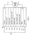
- FIG. 1 shows schematically the layer structure of the OLED device.
- the OLED device 100 of this invention comprises a substrate 101, an anode 102, a hole-injection layer (HIL) 103, a hole-transport layer (HTL) 104, an emissive layer (EML) 105, an electron-transport layer (ETL) 106, two buffer layers 107 and 108, and a cathode 109.
- HIL hole-injection layer
- HTL hole-transport layer
- EML emissive layer
- ETL electron-transport layer
- electroluminescence can be viewed from either the anode side or the cathode side.
- the intensity of the electroluminescence is dependent on the magnitude of the electrical current that is passed through the OLED device, which in term is dependent on the luminescent and electrical characteristics of the organic layers as well as the charge-injecting nature of the anode 102 and cathode 109.
- composition and the function of the various layers constituting the OLED device are described as follows:
- Substrate 101 may include glass, ceramic, or plastics. Since the OLED device fabrication does not require high temperature process, any substrate that can withstand process temperatures of the order of 100°C is useful, which includes most thermal plastics.
- the substrate may take the form of rigid plate, flexible sheet, or curved surfaces.
- Substrate 101 may include support with electronic backplane, and thus includes active-matrix substrates, which contain electronic addressing and switching elements. Examples of such active-matrix substrates include single-crystal silicon wafer with CMOS circuit elements, substrates with high-temperature polysilicon thin-film-transistors, substrates with low-temperature polysilicon thin-film transistors. CMOS circuit elements, substrates with high-temperature polysilicon thin-film-transistors, substrates with low-temperature polysilicon thin-film transistors. CMOS circuit elements, substrates with high-temperature polysilicon thin-film-transistors, substrates with low-temperature polysilicon thin-film transistors. CMOS circuit elements
- Anode 102 provides the function of injecting hole into the organic layer when a positive potential relative to the cathode is applied to the OLED. It has been shown, for example in commonly-assigned US-A-4,720,432 , that indium tin oxide (ITO) forms efficient anode because it has a relatively high work function. Since ITO film itself is transparent, ITO coated glass provides an excellent support for the fabrication of OLED devices.
- ITO coated glass provides an excellent support for the fabrication of OLED devices.
- Other suitable anode materials include high work function metals such as Au, Pt, Pd, or alloys of these metals.
- Hole-injection layer (HIL) 103 provides the function of increasing the efficiency of the hole-injection from the anode 102 into the organic layers. It has been shown, for example in commonly-assigned US-A-4,885,211 , that a porphorinic or phthalocyanine compound is useful as a hole injection layer 103, resulting in increased luminance efficiency and operational stability.
- HIL materials include CFx, which is a fluorinated polymer deposited by plasma-assisted vapor deposition, wherein x is less than or equal to 2 and greater than 0.
- HTL Hole-transport layer
- EML emissive layer
- HTL materials include various classes of aromatic amines as disclosed in commonly-assigned US-A-4,720,432 .
- a preferred class of HTL materials includes the tetraaryldiamines of formula (I). wherein:
- Useful selected (fused aromatic ring containing) aromatic tertiary amines are the following:
- Emissive layer 105 of FIG. 1 provides the function of light emission produced as a result of recombination of holes and electrons in this layer.
- a preferred embodiment of the emissive layer comprises of a host material doped with one or more fluorescent dyes. Using this host-dopant composition, highly efficient OLED devices can be constructed. Simultaneously, the color of the EL devices can be tuned by using fluorescent dyes of different emission wavelengths in a common host material. Tang and others in commonly-assigned US-A-4,769,292 has described this dopant scheme in considerable details for OLED devices using Alq as the host material.
- the emissive layer can contain a green light-emitting doped material, a blue light-emitting doped material, or a red light-emitting doped material.
- Preferred host materials include the class of 8-quinolinol metal chelate compounds with the chelating metals being A1, Mg, Li, Zn, for example.
- Another preferred class of host materials includes anthracene derivatives such as 9,10 dinaphthyl anthracene; 9,10 dianthryl anthracene; alkyl substituted 9,10 dinaphthyl anthracene, as disclosed in Shi and others commonly-assigned US-A-5,935,721 .
- Dopant materials include most fluorescent and phorphorescent dyes and pigments.
- Preferred dopant materials include coumarins such as Coumarin 6, dicyanomethylenepyrans such as 4-dicyanomethylene-4H pyrans, as disclosed in Tang and others commonly-assigned US-A-4,769,292 and in Chen and others in commonly-assigned US-A-6,020,078 .
- Electron-transport layer 106 of FIG. 1 provides the function of delivering electrons injected from the cathode to the emissive layer 105.
- Useful materials include Alq, benzazoles, as disclosed in commonly-assigned Shi and others commonly-assigned US-A-5,645,948 .
- Buffer layer 1 (107) and buffer layer 2 (108) of FIG. 1 provide the function of controlling the sputter damage during the deposition of the cathode and thereby preserve or enhance the performance of the OLED device. It has been found that both buffer layers are necessary in order to minimize the sputter damage.
- Buffer layer 1 which is adjacent to the electron-transport layer, includes materials belonging to the alkaline halide group. Preferred materials include LiF, NaCl, KI, CsF, and CsI. These materials are sublimable and can be deposited in a thin film form using conventional vapor deposition methods. Since they are electrical insulators, the useful range of thickness for buffer layer 1 using these materials should be no greater than 10 nm. The preferred range of thickness is less than 3 nm and greater than 0.1 nm.
- Buffer layer 2 (108) of FIG. 1 includes yttrium and manganese.
- Other useful materials include gallium, indium, lead, scandium, titanium, zirconium, hafnium, niobium, alkaline metals, alkaline earth metals and rare earth metals whose work functions are between 2.0 eV to 4.0 eV. Some of these materials can be deposited in a thin-film form using conventional vapor deposition methods; others have low vapor pressures requiring electron beam deposition. It will be shown in the examples of this invention, that in absence of buffer layer 1, buffer layer 2 is considerably less effective in reducing sputter damage, resulting in OLED devices with lower luminance efficiency and higher drive voltage.
- the buffer layer 1 is disposed adjacent to the electron-transport layer and the buffer layer 2 is disposed over buffer layer 1.
- the thickness of the buffer layer 2 should be in a range of less than 20 nm but greater than 0 nm.
- the preferred thickness for the buffer layer 2 is less than 10 nm but greater than 0 nm.
- the thickness of a bilayer buffer structure should be greater than 0 nm and less than 30 nm.
- the buffer structure thickness more preferably be greater 0 but less than 5 nm.
- the layer (109) of FIG. 1 provides increased conductivity and reflectivity of the electron-injecting layer of the device. Sputter deposition is preferred because it is a robust thin-film deposition process.
- the sputtering apparatus was equipped with a 5.1-cm (2-inch) diameter DC sputter gun and a 1 kW DC power supply.
- a target of pure Ag was used in these investigations although other metal and alloy targets can also be used.
- the target-to-substrate distance was 7,6 cm (3 inch).
- the chamber was evacuated to less than 133x10 -6 Pa (1x10 -6 Torr) and backfilled with pure Ar to maintain a fixed pressure, typically 2.1 Pa (16 mT).
- the sputtering power applied to the Ag target was 75 W, resulting in a film deposition rate of about 1.5 nm/s.
- the deposition parameters such as power and deposition time were varied in this investigation to produce the desired film thickness.
- FIG. 1 embodiment is believed preferred, it will be appreciated by those skilled in the art that a device can also be made which does not use hole-injection layer 103, hole-transport layer 104 and electron- transport layer 106.
- the emissive layer can be selected to include hole- transport and electron-transport functions and the anode layer can function as the hole-injection layer. In such an instance, the device requires 105 and does not require layers 103, 104, and 106.
- Table 2 compiled are the device structures and performances of devices including a device of the present invention and a control device.
- the ITO, HIL, HTL and EML/ETL of devices 100, 101, 102 and 103 are identical, and the organic layers, HIL and EML/ETL, were deposited in a single pump-down run.
- the device 100 has no buffer layer; Ag layer, 60 nm thick was directly sputtered on the Alq ETL layer. This device exhibits severely degraded performance, as evidenced by its unusually high operating voltage and extremely low efficiency. The degradation is likely due to damage induced during sputtering and may also because of high work function of Ag (Ag work function ⁇ 4.4 eV).
- the control device, 103 which was provided with a standard cathode consisting of a 60 nm thick electron beam evaporated A1 layer on a 0.5 nm LiF layer exhibits a luminance efficiency of 2.4 cd/A and an operating voltage of 5.4 volt.
- the device 101 was provided with an electron beam evaporated 1.5 nm thick Y metal buffer (work function ⁇ 3.4 eV) layer upon which a 60 nm thick Ag layer was sputtered under the same conditions as for the device 100.
- the device 101 shows an efficiency of 1.8 cd/A and an operating voltage of 6.9 V indicating markedly improved performances over those of the device 100.
- the performance of the device 101 falls short of that of the control device 103.
- the bilayer buffer structure in the device 102 is a bilayer buffer structure comprising a 1.5 nm Y layer on a 0.5 nm LiF layer.
- the bilayer buffer structure in the device 102 has resulted in an improvement amounting to 36% in efficiency and 0.8 V in operating voltage over those of the device 101 that has only one buffer layer.
- the device of the present invention, the bilayer buffer device 102 has efficiency of 2.5 cd/A that is identiacal to that of the control device 103.
- the operating voltage of the bilayer device is slightly higher than that of the control device, but variation in device structure and uncertainty of measurement may account for the discrepancy. Thus, it is believed, that the bilayer buffer has eliminated or greatly reduced the sputtering damage.
- Table 2 includes the device structures and performances of another set of devices including a device of the present invention and a control device.
- ITO, HIL, HTL and EML/ETL of devices 301, 302 and 303 are identical, and the organic layers, HIL and EML/ETL, were deposited in a single pump-down run.
- the control device 303 for this batch was also provided with a standard cathode comprising a 60 nm evaporated A1 layer on a 0.5 nm LiF layer. This device exhibits a luminance efficiency of 2.5 cd/A and an operating voltage of 5.6 volt.
- the device 301 was provided with a 1.5 nm thick Y metal buffer layer upon which a Ag layer, 60 nm thick, was sputtered under the same conditions as for the devices of example 1.
- the device 301 shows an efficiency of 1.9 cd/A and an operating voltage of 7.2 V.
- the performance of the device 301 falls short of that of the control device 303.
- In the structure of device 302 incorporated a bilayer buffer structure comprising a 1.5 nm Y layer on a 0.5 nm LiF layer.
- the bilayer buffer in the device 302 has resulted in an improvement amounting to 33% in efficiency and 1.2 V in the operating voltage over the device 301 that has only LiF buffer layer.
- the bilayer buffer device 302 has efficiency 2.5 cd/A that is identiacal to that of the control device 303.
- the operating voltage of the bilayer device is 0.4 V higher than that of the control device, and the discrepancy is most likely due variation in device structure and uncertainty of measurements.
- the bilayer buffer has eliminated or greatly reduced the damage during sputtering deposition of the overlayer.
- Table 3 includes the device structure and performance of a control device along with several devices of the present invention that use a different buffer structure.
- the HTL and EML/ETL of devices 201, 202, and 103 were again identical, and were deposited in a single pump-down run.
- the control device 103 was provided with a standard cathode comprising a 60 nm evaporated A1 layer on a 0.5 nm LiF layer. This device exhibited luminance efficiency of 2.4 cd/A and an operating voltage of 5.4 volt.
- the device 201 was provided with a 1.5 nm thick thermally evaporated Mn metal buffer ( Mn work function ⁇ 3.8 eV) layer upon which a Ag layer, 60 nm thick, was sputtered under the same condition as that for the devices of example 1.
- the device 201 shows an efficiency of 1.8 cd/A and an operating voltage of 6.8 V.
- the performance of the device 201 falls short of that of the control device 103.
- the structure of device 202 incorporated a buffer structure comprising a 1.5 nm Mn layer on a 0.5 nm LiF layer.
- the bilayer buffer in the device 202 has resulted in an improvement amounting to 20% in efficiency and 0.9 V in the operating voltage over the device 201 that has only LiF buffer layer.
- the device of the present invention has an efficiency of 2.1 cd/A that is close to that of the control device 103.
- the operating voltage of the bilayer device is 0.5 V higher than that of the control device and the discrepancy can be due to variation in device sructure and uncertainty of measurement.
- the bilayer buffer has greatly reduced the damage during sputtering deposition of the overlayer.
- Table 3 includes the device structures and performances of another set of devices of the present invention and a control device.
- ITO, HIL, HTL and EML/ETL of devices 401, 402 and 403 are identical, and the organic layers, HIL and EML/ETL, were deposited in a single pump-down run.
- the control device 403 for this batch was also provided with a standard cathode comprising a 60 nm evaporated A1 layer on a 0.5 nm LiF layer. This device exhibits a luminance efficiency of 2.5 cd/A and an operating voltage of 5.8 volt.
- the device 401 was provided with a 1.5 nm thick Mn metal buffer layer upon which a Ag layer, 60 nm thick, was sputtered under the same conditions as for the devices of example 1.
- the device 401 shows an efficiency of 1.9 cd/A and an operating voltage of 6.9 V.
- the performance of the device 401 falls short of that of the control device 403.
- In the structure of device 402 incorporated a bilayer buffer structure comprising a 1.5 nm Mn layer on a 0.5 nm LiF layer.
- the bilayer buffer in the device 402 has resulted in an improvement amounting to 33% in efficiency and 0.7 V in the operating voltage over the device 401 that has only LiF buffer layer.
- the bilayer buffer device 402 has efficiency 2.2 cd/A that is close to that of the control device 403.
- the operating voltage of the bilayer device is 0.6 V higher than that of the control device and the discrepancy may be due to difference in device structure and uncertainty of measurements.
- the bilayer buffer has eliminated or greatly reduced the damage during sputtering deposition of the overlayer.
- a bilayer buffer structure comprising a low work function layer on a LiF layer can be very effective in protecting the organic active layers from damage during sputtering deposition of the overlying electrode. It is noted that an ultrathin buffer structure amounting to only a few nanometers is adequate for virtual elimination of sputter damage.
- the sputtered electrode device is essentially equal in performance to the evaporated cathode device.
Landscapes
- Physics & Mathematics (AREA)
- Optics & Photonics (AREA)
- Electroluminescent Light Sources (AREA)
Description
- The present invention relates to organic light-emitting diode devices and methods for making such devices, which use an inorganic buffer structure and a sputtered metal or metal alloy layer on such inorganic buffer structure.
- Organic electroluminescent (OEL) device, alternately known as organic light emitting diode (OLED), is useful in flat-panel display applications. This light-emissive device is attractive because it can be designed to produce red, green, and blue colors with high luminance efficiency; it is operable with a low driving voltage of the order of a few volts and viewable from oblique angles. These unique attributes are derived from a basic OLED structure comprising of a multilayer stack of thin films of small-molecule organic materials sandwiched between an anode and a cathode. Tang and others in commonly-assigned
US-A-4,769,292 andUS-A-4,885,211 have disclosed such a structure. The common electroluminescent (EL) medium is comprised of a bilayer structure of a hole-transport (HTL) layer and an electron-transport layer (ETL), typically of the order of a few tens of nanometer (nm) thick for each layer. The anode material is usually an optically transparent indium tin oxide (ITO) film on glass, which also serves as the substrate for the OLED. The cathode is typically a reflective thin film. Selection of electrode materials is based on work functions. ITO is most commonly used as the anode because it has a high work function. Mg:Ag alloys are generally used as electron-injecting contacts because they have lower work functions. Lithium containing alloys such as Al:Li, Ag:Li and LiF/Al contacts also provide efficient electron injection. The device emits visible light in response to a potential difference applied across the EL medium. When an electrical potential difference is applied at the electrodes the injected carriers- hole at the anode and electron at the cathode -migrate towards each other through EL medium and a fraction of them recombine to emit light. - In the fabrication of OLED vapor deposition method is used. Using this method, the organic layers are deposited in thin-film form onto the ITO glass substrates in a vacuum chamber, followed by the deposition of the cathode layer. Among the deposition methods for the cathode, vacuum deposition using resistive heating or electron-beam heating has been found to be most suitable because it does not cause damage to the organic layers. However, it would be highly desirable to avoid these methods for fabrication of the cathode layer. This is because they are inefficient processes. In order to realize low-cost manufacturing one must adopt and develop a proven robust high-throughput process specific to OLED fabrication. Sputtering has been used as a method of choice for thin film deposition in many industries. Conformal, dense, and adherent coatings, short cycle time, low maintenance of coating chamber, efficient use of materials are among few of the benefits of sputtering.
- The fabrication of the OLED cathode layer employing high-energy deposition process such as sputtering is not commonly practiced because of the potential damage inflicted on the organic layers, and thus degradation of the OLED performance. Sputter deposition takes place in a complex environment that comprises of energetic neutrals, electrons, positive and negative ions and emissions from the excited states that can degrade the organic layers upon which the cathode is deposited.
- Liao and others (Appl. Phys. Lett. 75,1619 [1999]) investigated using x-ray and ultraviolet photoelectron spectroscopies the damages induced on Alq surfaces by 100 eV Ar + irradiation. It is revealed from core level electron density curves that some N-Al and C-O-Al bonds in Alq molecules were broken. The valance band structure is also tremendously changed implying the formation of a metal-like conducting surface. It is suggested that this would cause nonradiative quenching in OLEDs when electrons are injected into the Alq layer from the cathode and also would results in electrical shorts.
- During sputter deposition of cathode the Alq surface is subjected to high doses of Ar+ bombardments at several hundred volts. As shown by Hung and others (J. Appl. Phys. 86, 4607 [1999]) that a dose only of 9 x 10¹⁴/cm2 altered the valance band structure. However, sputtering a cathode on Alq surface in Ar atmosphere would degrade the device performance.
- Sputtering damage is somewhat controllable, at least to some extent, by properly selecting the deposition parameters. In the European patent applications
EP 0 876 086 A2 ,EP 0 880 305 A1 , andEP 0 880 307 A2, Nakaya and others of TDK Corporation disclose a method of depositing a cathode by a sputtering technique. After depositing all organic layers, with vacuum still kept, the devices was transferred from the evaporation to a sputtering system wherein the cathode layer was deposited directly on the emission layer. The cathode was an A1 alloy comprised of 0.1 - 20 a% Li that additionally contained at least one of Cu, Mg and Zr in small amounts and in some cases had a protective overcoat. The OLED devices thus prepared using no buffer layer were claimed to have good adhesion at the organic layer/electrode interface, low drive voltage, high efficiency and exhibited a slower rate of development of dark spot. Grothe and others in patent applicationDE 198 07 370 C1 also disclose a sputtered cathode of an A1:Li alloy which had relatively high Li content and having one or more additional elements chosen from Mn, Pb, Pd, Si, Sn, Zn, Zr, Cu and SiC. In all of those examples no buffer was used, yet electroluminescent was produced at lower voltage. Some sputtering damage was possibly controlled by employing a low deposition rate. It is easily anticipated that by lowering sputtering power the damage inflicted on the organic layers can be reduced. At low power, however, the deposition rate can be impracticably low and the advantages of sputtering are reduced or even neutralized. - To minimize damage during high speed sputtering of cathodes a protective coating on the electron-transport layer can be useful. The protective layer, alternately termed as the buffer layer, must be robust to be effective. However, in addition to being resistant to plasma, the buffer layer must not interfere with the operation of the device and must preserve the device performance. Parthasarathy and others (J. Appl. Phys. 72, 2138 [1998]) reported an application of a buffer layer consisting of copper phthalocyanine (CuPc) and zinc phthalocyanine (ZnPc) during sputtering deposition of a metal free cathode. The buffer layer prevented damage to the underlying organic layers during the sputtering process. Hung and others (J. Appl. Phys. 86, 4607 [1999]) disclosed the application of CuPc buffer layers that permitted high-energy deposition of a cathode. The cathode contained a dopant, for example Li, which was believed to diffuse through the buffer layer and provided an electron injecting layer between the organic light emitting structure and the buffer layer. In the patent application
EP 0 982 783 A2 Nakaya and others disclose a cathode of A1:Li alloy. The cathode was prepared by sputtering using a buffer layer constructed of a porphyrin or napthacene compound that was deposed between the emission and the cathode. The device containing the sputtered electrode exhibited low drive voltage, high efficiency and retarted dark spot growth. Although it was claimed in all those references that efficient devices were made, none were said to have eliminated the sputter damage. - In the patent application
EP 1 076 368 A2 Hung and others disclose an OLED device structure comprising an electron-transporting layer, a thin layer of metal fluorides or oxides, a thin Al layer and a semitransparent metal layer consisting of silver, gold, copper and their alloys. - The shortcomings of prior art device structures are that they are not ideally suited for devices that contain dopants emitting in different colors. While CuPc is largely transparent in the green region of the wavelength, the transparency in red and blue wavelength length regions is substantially lower. To be useful in full color devices the buffer should have uniformity of transparency in a greater range of wavelength. Another undesirable feature is that the phthalocyanine layer must be about 20 nm thick requiring long deposition time.
- It is therefore an object of the present invention to provide an OLED device structure, which has relatively uniform transparency in the visible wavelength range and that, offers significant protection against damage during sputtering deposition of electrode.
- The above object was achieved in an OLED device as described in claim 1.
- An advantage of the present invention is that damage to the organic layers during sputtering deposition of cathodes is minimized. The present invention permits high sputtering rates and is suitable for full color large-area devices and displays.
- The buffer structure in accordance with the invention having two buffer layers exhibited substantially superior performance in comparison to that of devices having only the metal/metal alloy buffer layer but otherwise identical in structure.
- The buffer structure is very thin and has relatively uniform transparency in the visible wavelength range and that offers significant protection against damage during sputtering deposition of cathodes
- Another advantage of the present invention is that OLED devices produced by the sputtering deposition method are efficient and operable with a low drive voltage.
-
FIG. 1 shows schematically the layer structure of the OLED device. - Throughout the ensuring description acronyms are used to designate the names of different layers and operating features of organic light-emitting diode devices. For reference, they are listed in Table 1.
Table 1 OLED Organic light-emitting diode ITO Indium tin oxide HIL Hole-injection layer HTL Hole-transport layer EML Emissive layer ETL Electron- transport layer NPB 4,4'-Bis[N-(1-naphthyl)-N-phenylamino]biphenyl (NPB) Alq Tris(8-hydroxyquinoline) aluminum LiF Lithium Fluoride Y Yttrium Mn Manganese Mg:Ag Magnesium silver alloy Al Aluminum Ag Silver - Turning now to
FIG. 1 , theOLED device 100 of this invention comprises asubstrate 101, ananode 102, a hole-injection layer (HIL) 103, a hole-transport layer (HTL) 104, an emissive layer (EML) 105, an electron-transport layer (ETL) 106, twobuffer layers cathode 109. In operation, the anode and the cathode are connected to avoltage source 110 viaconductors 111 and electrical current is passed through the organic layers, resulting in light emission or electroluminescence from the OLED device. Depending on the optical transparency of the anode and cathode, electroluminescence can be viewed from either the anode side or the cathode side. The intensity of the electroluminescence is dependent on the magnitude of the electrical current that is passed through the OLED device, which in term is dependent on the luminescent and electrical characteristics of the organic layers as well as the charge-injecting nature of theanode 102 andcathode 109. - The composition and the function of the various layers constituting the OLED device are described as follows:
-
Substrate 101 may include glass, ceramic, or plastics. Since the OLED device fabrication does not require high temperature process, any substrate that can withstand process temperatures of the order of 100°C is useful, which includes most thermal plastics. The substrate may take the form of rigid plate, flexible sheet, or curved surfaces.Substrate 101 may include support with electronic backplane, and thus includes active-matrix substrates, which contain electronic addressing and switching elements. Examples of such active-matrix substrates include single-crystal silicon wafer with CMOS circuit elements, substrates with high-temperature polysilicon thin-film-transistors, substrates with low-temperature polysilicon thin-film transistors. Those skilled in the art will appreciate that other circuit elements can be used to address and drive the OLED devices. -
Anode 102 provides the function of injecting hole into the organic layer when a positive potential relative to the cathode is applied to the OLED. It has been shown, for example in commonly-assignedUS-A-4,720,432 , that indium tin oxide (ITO) forms efficient anode because it has a relatively high work function. Since ITO film itself is transparent, ITO coated glass provides an excellent support for the fabrication of OLED devices. Other suitable anode materials include high work function metals such as Au, Pt, Pd, or alloys of these metals. - Hole-injection layer (HIL) 103 provides the function of increasing the efficiency of the hole-injection from the
anode 102 into the organic layers. It has been shown, for example in commonly-assignedUS-A-4,885,211 , that a porphorinic or phthalocyanine compound is useful as ahole injection layer 103, resulting in increased luminance efficiency and operational stability. Other preferred HIL materials include CFx, which is a fluorinated polymer deposited by plasma-assisted vapor deposition, wherein x is less than or equal to 2 and greater than 0. - Hole-transport layer (HTL) 104 provides the function of transporting holes to the emissive layer (EML) 105. HTL materials include various classes of aromatic amines as disclosed in commonly-assigned
US-A-4,720,432 . A preferred class of HTL materials includes the tetraaryldiamines of formula (I).
- Ar, Ar1, Ar2 and Ar3 are independently selected from among phenyl, biphenyl and naphthyl moieties;
- L is a divalent naphthylene moiety or dn;
- d is a phenylene moiety;
- n is an integer of from 1 to 4; and
- at least one of Ar, Ar1, Ar2 and Ar3 is a naphthyl moiety.
- Useful selected (fused aromatic ring containing) aromatic tertiary amines are the following:
- 4,4'-Bis[N-(1-naphthyl)-N-phenylamino]biphenyl (NPB)
- 4,4"-Bis[N-(1-naphthyl)-N-phenylamino]-p-terphenyl
- 4,4'-Bis[N-(2-naphthyl)-N-phenylamino]biphenyl
- 1,5-Bis[N-(1-naphthyl)-N-phenylamino]naphthalene
- 4,4'-Bis[N-(2-pyrenyl)-N-phenylamino]bi-phenyl
- 4,4'-Bis[N-(2-perylenyl)-N-phenylamino]biphenyl
- 2,6-Bis(di-p-tolylamino)naphthalene
- 2,6-Bis[di-(1-naphtyl)amino]naphthalene
-
Emissive layer 105 ofFIG. 1 provides the function of light emission produced as a result of recombination of holes and electrons in this layer. A preferred embodiment of the emissive layer comprises of a host material doped with one or more fluorescent dyes. Using this host-dopant composition, highly efficient OLED devices can be constructed. Simultaneously, the color of the EL devices can be tuned by using fluorescent dyes of different emission wavelengths in a common host material. Tang and others in commonly-assignedUS-A-4,769,292 has described this dopant scheme in considerable details for OLED devices using Alq as the host material. As set forth in the Tang and others commonly-assignedUS-A-4,769,292 , the emissive layer can contain a green light-emitting doped material, a blue light-emitting doped material, or a red light-emitting doped material. - Preferred host materials include the class of 8-quinolinol metal chelate compounds with the chelating metals being A1, Mg, Li, Zn, for example. Another preferred class of host materials includes anthracene derivatives such as 9,10 dinaphthyl anthracene; 9,10 dianthryl anthracene; alkyl substituted 9,10 dinaphthyl anthracene, as disclosed in Shi and others commonly-assigned
US-A-5,935,721 . - Dopant materials include most fluorescent and phorphorescent dyes and pigments. Preferred dopant materials include coumarins such as Coumarin 6, dicyanomethylenepyrans such as 4-dicyanomethylene-4H pyrans, as disclosed in Tang and others commonly-assigned
US-A-4,769,292 and in Chen and others in commonly-assignedUS-A-6,020,078 . - Electron-
transport layer 106 ofFIG. 1 provides the function of delivering electrons injected from the cathode to theemissive layer 105. Useful materials include Alq, benzazoles, as disclosed in commonly-assigned Shi and others commonly-assignedUS-A-5,645,948 . - Buffer layer 1 (107) and buffer layer 2 (108) of
FIG. 1 provide the function of controlling the sputter damage during the deposition of the cathode and thereby preserve or enhance the performance of the OLED device. It has been found that both buffer layers are necessary in order to minimize the sputter damage. Buffer layer 1, which is adjacent to the electron-transport layer, includes materials belonging to the alkaline halide group. Preferred materials include LiF, NaCl, KI, CsF, and CsI. These materials are sublimable and can be deposited in a thin film form using conventional vapor deposition methods. Since they are electrical insulators, the useful range of thickness for buffer layer 1 using these materials should be no greater than 10 nm. The preferred range of thickness is less than 3 nm and greater than 0.1 nm. - Buffer layer 2 (108) of
FIG. 1 includes yttrium and manganese. Other useful materials include gallium, indium, lead, scandium, titanium, zirconium, hafnium, niobium, alkaline metals, alkaline earth metals and rare earth metals whose work functions are between 2.0 eV to 4.0 eV. Some of these materials can be deposited in a thin-film form using conventional vapor deposition methods; others have low vapor pressures requiring electron beam deposition. It will be shown in the examples of this invention, that in absence of buffer layer 1,buffer layer 2 is considerably less effective in reducing sputter damage, resulting in OLED devices with lower luminance efficiency and higher drive voltage. The provision of both buffer layer 1 andbuffer layer 2 is required in accordance with the invention to minimize cathode sputter damage. The advantageous results from using these two layers are indeed quite unexpected. The buffer layer 1 is disposed adjacent to the electron-transport layer and thebuffer layer 2 is disposed over buffer layer 1. The thickness of thebuffer layer 2 should be in a range of less than 20 nm but greater than 0 nm. The preferred thickness for thebuffer layer 2 is less than 10 nm but greater than 0 nm. The thickness of a bilayer buffer structure should be greater than 0 nm and less than 30 nm. The buffer structure thickness more preferably be greater 0 but less than 5 nm. The layer (109) ofFIG. 1 provides increased conductivity and reflectivity of the electron-injecting layer of the device. Sputter deposition is preferred because it is a robust thin-film deposition process. - The sputtering apparatus was equipped with a 5.1-cm (2-inch) diameter DC sputter gun and a 1 kW DC power supply. A target of pure Ag was used in these investigations although other metal and alloy targets can also be used. The target-to-substrate distance was 7,6 cm (3 inch). The chamber was evacuated to less than 133x10-6 Pa (1x10⁻⁶ Torr) and backfilled with pure Ar to maintain a fixed pressure, typically 2.1 Pa (16 mT). The sputtering power applied to the Ag target was 75 W, resulting in a film deposition rate of about 1.5 nm/s. The deposition parameters such as power and deposition time were varied in this investigation to produce the desired film thickness. Although sputtering from a single target was used, simultaneous sputtering of multiple targets can be employed for increased process throughput. RF, Instead of DC, can be used as an alternate power source. It is conceived that instead of a metal layer an alloy layer with improved properties can be utilized. It is also understood that cosputtering of several targets instead of a single alloy target can be employed for adjusting the composition of the alloy layer.
- Although the
FIG. 1 embodiment is believed preferred, it will be appreciated by those skilled in the art that a device can also be made which does not use hole-injection layer 103, hole-transport layer 104 and electron-transport layer 106. Those skilled in the art will appreciate that the emissive layer can be selected to include hole- transport and electron-transport functions and the anode layer can function as the hole-injection layer. In such an instance, the device requires 105 and does not requirelayers - In the following examples, reference should be made to Table 1 for the appropriate structure and operating parameters corresponding to the listed acronym. In these tables V (volt) refers to the voltage required to pass 20 mA/cm2 through the device, and L (cd/m2) refers to the luminance of the OLED device under this condition. Moreover, Tables, 2 and 3, which follow, will be referenced in the following examples.
Table 2 Structure, Layer Thickness and Performance of OLED Devices with LiF/Al Standard Cathode and Sputtered Ag Layer on LiF/Y Bilayer Buffer Device ID Anode ITO Thickness (nm) HIL CFx Thickness (nm) HTL NPB Thickness (nm) EML/ETL Alq Thickness (nm) Buffer 1 LIF Thickness (nm) Buffer 2 Y Thickness (nm) Al cathode Thickness (nm) Evaporated Ag reflector Thickness (nm) Sputtered Volt EL(Cd/ m2) 100 42 1 75 60 60 10.2 1 101 42 1 75 60 1.5 60 6.9 368 102 42 1 75 60 0.5 1.5 60 6.1 499 103 42 1 75 60 0.5 60 5.4 484 301 42 1 75 60 1.5 60 7.2 382 302 42 1 75 60 0.5 1.5 60 6.0 507 303 42 1 75 60 0.5 60 5.6 490 Table 3 Structure, Layer Thickness and Performance of OLED Devices with LiF/Al Standard Cathode and Sputtered Ag Layer on LiF/Mn Bilayer Buffer Device ID Anode ITO Thickness (nm) HIL CFx Thickness (nm) HTL NPB Thickness (nm) EML/ETL Alq Thickness (nm) Buffer 1 LIF Thickness (nm) Buffer 2 Mn Thickness (nm) Al cathode Thickness (nm) Evaporated Ag reflector Thickness (nm) Sputtered Volt EL (Cd/m2) 201 42 1 75 60 1.5 60 6.8 355 202 42 1 75 60 0.5 1.5 60 5.9 427 103 42 1 75 60 0.5 60 5.4 484 401 42 1 75 60 1.5 60 6.9 383 402 42 1 75 60 0.5 1.5 60 6.2 449 403 42 1 75 60 0.5 60 5.8 499 - In Table 2 compiled are the device structures and performances of devices including a device of the present invention and a control device. The ITO, HIL, HTL and EML/ETL of
devices device 100 has no buffer layer; Ag layer, 60 nm thick was directly sputtered on the Alq ETL layer. This device exhibits severely degraded performance, as evidenced by its unusually high operating voltage and extremely low efficiency. The degradation is likely due to damage induced during sputtering and may also because of high work function of Ag (Ag work function ∼ 4.4 eV). The control device, 103, which was provided with a standard cathode consisting of a 60 nm thick electron beam evaporated A1 layer on a 0.5 nm LiF layer exhibits a luminance efficiency of 2.4 cd/A and an operating voltage of 5.4 volt. Thedevice 101 was provided with an electron beam evaporated 1.5 nm thick Y metal buffer (work function ∼ 3.4 eV) layer upon which a 60 nm thick Ag layer was sputtered under the same conditions as for thedevice 100. Thedevice 101 shows an efficiency of 1.8 cd/A and an operating voltage of 6.9 V indicating markedly improved performances over those of thedevice 100. The performance of thedevice 101, however, falls short of that of thecontrol device 103. In structure of thedevice 102 incorporated is a bilayer buffer structure comprising a 1.5 nm Y layer on a 0.5 nm LiF layer. The bilayer buffer structure in thedevice 102 has resulted in an improvement amounting to 36% in efficiency and 0.8 V in operating voltage over those of thedevice 101 that has only one buffer layer. The device of the present invention, thebilayer buffer device 102, has efficiency of 2.5 cd/A that is identiacal to that of thecontrol device 103. The operating voltage of the bilayer device is slightly higher than that of the control device, but variation in device structure and uncertainty of measurement may account for the discrepancy. Thus, it is believed, that the bilayer buffer has eliminated or greatly reduced the sputtering damage. - Table 2 includes the device structures and performances of another set of devices including a device of the present invention and a control device. Again the ITO, HIL, HTL and EML/ETL of devices 301, 302 and 303 are identical, and the organic layers, HIL and EML/ETL, were deposited in a single pump-down run. The control device 303 for this batch was also provided with a standard cathode comprising a 60 nm evaporated A1 layer on a 0.5 nm LiF layer. This device exhibits a luminance efficiency of 2.5 cd/A and an operating voltage of 5.6 volt. The device 301 was provided with a 1.5 nm thick Y metal buffer layer upon which a Ag layer, 60 nm thick, was sputtered under the same conditions as for the devices of example 1. The device 301 shows an efficiency of 1.9 cd/A and an operating voltage of 7.2 V. The performance of the device 301, however, falls short of that of the control device 303. In the structure of device 302 incorporated a bilayer buffer structure comprising a 1.5 nm Y layer on a 0.5 nm LiF layer. The bilayer buffer in the device 302 has resulted in an improvement amounting to 33% in efficiency and 1.2 V in the operating voltage over the device 301 that has only LiF buffer layer. The device of the present invention, the bilayer buffer device 302 has efficiency 2.5 cd/A that is identiacal to that of the control device 303. The operating voltage of the bilayer device is 0.4 V higher than that of the control device, and the discrepancy is most likely due variation in device structure and uncertainty of measurements. Thus, the bilayer buffer has eliminated or greatly reduced the damage during sputtering deposition of the overlayer.
- Table 3 includes the device structure and performance of a control device along with several devices of the present invention that use a different buffer structure. The HTL and EML/ETL of
devices 201, 202, and 103 were again identical, and were deposited in a single pump-down run. Thecontrol device 103 was provided with a standard cathode comprising a 60 nm evaporated A1 layer on a 0.5 nm LiF layer. This device exhibited luminance efficiency of 2.4 cd/A and an operating voltage of 5.4 volt. The device 201 was provided with a 1.5 nm thick thermally evaporated Mn metal buffer ( Mn work function ∼ 3.8 eV) layer upon which a Ag layer, 60 nm thick, was sputtered under the same condition as that for the devices of example 1. The device 201 shows an efficiency of 1.8 cd/A and an operating voltage of 6.8 V. The performance of the device 201, however, falls short of that of thecontrol device 103. In the structure of device 202 incorporated a buffer structure comprising a 1.5 nm Mn layer on a 0.5 nm LiF layer. The bilayer buffer in the device 202 has resulted in an improvement amounting to 20% in efficiency and 0.9 V in the operating voltage over the device 201 that has only LiF buffer layer. The device of the present invention, the bilayer buffer device 202, has an efficiency of 2.1 cd/A that is close to that of thecontrol device 103. The operating voltage of the bilayer device is 0.5 V higher than that of the control device and the discrepancy can be due to variation in device sructure and uncertainty of measurement. Thus the bilayer buffer has greatly reduced the damage during sputtering deposition of the overlayer. - Table 3 includes the device structures and performances of another set of devices of the present invention and a control device. Again the ITO, HIL, HTL and EML/ETL of devices 401, 402 and 403 are identical, and the organic layers, HIL and EML/ETL, were deposited in a single pump-down run. The control device 403 for this batch was also provided with a standard cathode comprising a 60 nm evaporated A1 layer on a 0.5 nm LiF layer. This device exhibits a luminance efficiency of 2.5 cd/A and an operating voltage of 5.8 volt. The device 401 was provided with a 1.5 nm thick Mn metal buffer layer upon which a Ag layer, 60 nm thick, was sputtered under the same conditions as for the devices of example 1. The device 401 shows an efficiency of 1.9 cd/A and an operating voltage of 6.9 V. The performance of the device 401, however, falls short of that of the control device 403. In the structure of device 402 incorporated a bilayer buffer structure comprising a 1.5 nm Mn layer on a 0.5 nm LiF layer. The bilayer buffer in the device 402 has resulted in an improvement amounting to 33% in efficiency and 0.7 V in the operating voltage over the device 401 that has only LiF buffer layer. The device of the present invention, the bilayer buffer device 402 has efficiency 2.2 cd/A that is close to that of the control device 403. The operating voltage of the bilayer device is 0.6 V higher than that of the control device and the discrepancy may be due to difference in device structure and uncertainty of measurements. Thus, the bilayer buffer has eliminated or greatly reduced the damage during sputtering deposition of the overlayer.
- Above examples show that an ultrathin single-layer buffer of low work function materials deposited over the Alq electron-transport layer offers some protection for the EL medium against sputtering damage. In accordance with the present invention, a bilayer buffer structure comprising a low work function layer on a LiF layer can be very effective in protecting the organic active layers from damage during sputtering deposition of the overlying electrode. It is noted that an ultrathin buffer structure amounting to only a few nanometers is adequate for virtual elimination of sputter damage. The sputtered electrode device is essentially equal in performance to the evaporated cathode device.
Claims (10)
- An OLED device, comprising:a) a substrate (101);b) an anode (102) formed of a conductive material over the substrate;c) an emissive layer (105) having an electroluminescent material provided over the anode layer;d) an electron-transport layer provided over the emissive layer; characterised bye) a buffer structure including at least two layers, a first buffer layer (107) provided over the electron-transport layer and containing an alkaline halide and a second buffer layer (108) provided over the first buffer layer and containing a metal or metal alloy and having a work function of between 2.0 to 4.0 eV; andf) a sputtered layer (109) of a metal or metal alloy provided over the buffer structure.
- The OLED device of claim 1, further comprisinga hole-injection layer (103) provided over the anode layer;and a hole-transport layer (104) provided over the hole-injection layer;the emissive layer being provided over the hole-transport layer.
- The OLED device of claim 1 wherein the first buffer layer has a thickness less than 10 nm but greater than 0 nm.
- The OLED device of claim 1 wherein the first buffer layer has a thickness less than 3 nm but greater than 0.1 nm.
- The OLED device of claim 1 wherein the second buffer layer has a thickness less than 20 nm but greater than 0 nm.
- The OLED device of claim 1 wherein the second buffer layer has a thickness less than 10 nm but greater than 0 nm.
- The OLED device of claim 1 wherein the alkaline halide includes LiF.
- The OLED device of claim 1 wherein the metal having a work function between 2.0 eV to 4.0 eV includes yttrium, manganese, gallium, indium, lead, scandium, titanium, zirconium, hafnium, niobium, alkaline metals, alkaline earth metals and rare earth metals or metal alloys thereof.
- The OLED device of claim 1 wherein the sputtered layer includes silver, aluminum, copper and, gold and alloys thereof.
- The OLED device of claim 1 wherein the electron-transport layer includes Alq.
Applications Claiming Priority (2)
| Application Number | Priority Date | Filing Date | Title |
|---|---|---|---|
| US09/795,265 US6551725B2 (en) | 2001-02-28 | 2001-02-28 | Inorganic buffer structure for organic light-emitting diode devices |
| US795265 | 2001-02-28 |
Publications (3)
| Publication Number | Publication Date |
|---|---|
| EP1237208A2 EP1237208A2 (en) | 2002-09-04 |
| EP1237208A3 EP1237208A3 (en) | 2006-06-14 |
| EP1237208B1 true EP1237208B1 (en) | 2009-04-15 |
Family
ID=25165140
Family Applications (1)
| Application Number | Title | Priority Date | Filing Date |
|---|---|---|---|
| EP02075666A Expired - Lifetime EP1237208B1 (en) | 2001-02-28 | 2002-02-18 | Inorganic buffer structure for organic light-emitting diode devices |
Country Status (4)
| Country | Link |
|---|---|
| US (1) | US6551725B2 (en) |
| EP (1) | EP1237208B1 (en) |
| JP (1) | JP2002260862A (en) |
| DE (1) | DE60231931D1 (en) |
Families Citing this family (57)
| Publication number | Priority date | Publication date | Assignee | Title |
|---|---|---|---|---|
| JP4472056B2 (en) * | 1999-07-23 | 2010-06-02 | 株式会社半導体エネルギー研究所 | Electroluminescence display device and manufacturing method thereof |
| JP4053260B2 (en) * | 2000-10-18 | 2008-02-27 | シャープ株式会社 | Organic electroluminescence display element |
| TW533446B (en) * | 2000-12-22 | 2003-05-21 | Koninkl Philips Electronics Nv | Electroluminescent device and a method of manufacturing thereof |
| US7071615B2 (en) * | 2001-08-20 | 2006-07-04 | Universal Display Corporation | Transparent electrodes |
| JP3804858B2 (en) * | 2001-08-31 | 2006-08-02 | ソニー株式会社 | Organic electroluminescent device and manufacturing method thereof |
| US20030129447A1 (en) * | 2001-09-19 | 2003-07-10 | Eastman Kodak Company | Sputtered cathode having a heavy alkaline metal halide-in an organic light-emitting device structure |
| JP4011325B2 (en) * | 2001-10-31 | 2007-11-21 | パイオニア株式会社 | Organic electroluminescence device |
| JP2003187972A (en) * | 2001-12-20 | 2003-07-04 | Dainippon Printing Co Ltd | Method for manufacturing organic EL element and organic EL transfer member and transfer object |
| US6835947B2 (en) * | 2002-01-31 | 2004-12-28 | Hewlett-Packard Development Company, L.P. | Emitter and method of making |
| US20040031965A1 (en) * | 2002-08-16 | 2004-02-19 | Forrest Stephen R. | Organic photonic integrated circuit using an organic photodetector and a transparent organic light emitting device |
| TWI282701B (en) * | 2002-08-16 | 2007-06-11 | Au Optronics Corp | Organic electroluminescent device |
| JP3706605B2 (en) * | 2002-09-27 | 2005-10-12 | 三洋電機株式会社 | Organic electroluminescence device and method for manufacturing the same |
| JP2006502537A (en) * | 2002-10-07 | 2006-01-19 | コーニンクレッカ フィリップス エレクトロニクス エヌ ヴィ | Manufacturing method of light emitting display |
| US6911961B2 (en) | 2002-10-11 | 2005-06-28 | Eastman Kodak Company | Method of designing an OLED display with lifetime optimized primaries |
| JP4216572B2 (en) * | 2002-11-20 | 2009-01-28 | 株式会社東芝 | Organic EL element and organic EL display device |
| CA2412379A1 (en) * | 2002-11-22 | 2004-05-22 | Luxell Technolgies Inc. | Transparent-cathode for top-emission organic light-emitting diodes |
| TWI232066B (en) * | 2002-12-25 | 2005-05-01 | Au Optronics Corp | Manufacturing method of organic light emitting diode for reducing reflection of external light |
| JP3859155B2 (en) * | 2003-03-06 | 2006-12-20 | 富士電機ホールディングス株式会社 | Organic EL device and method for manufacturing the same |
| WO2004082338A1 (en) * | 2003-03-13 | 2004-09-23 | Fujitsu Limited | Organic electroluminescence device and organic electroluminescence display |
| US7053412B2 (en) * | 2003-06-27 | 2006-05-30 | The Trustees Of Princeton University And Universal Display Corporation | Grey scale bistable display |
| GB2404284B (en) * | 2003-07-10 | 2007-02-21 | Dainippon Printing Co Ltd | Organic electroluminescent element |
| US6818329B1 (en) * | 2003-10-03 | 2004-11-16 | Eastman Kodak Company | Organic electroluminescent devices having a metal sub-layer within a hole-transporting region |
| JP2005183013A (en) * | 2003-12-16 | 2005-07-07 | Casio Comput Co Ltd | Display element, display device, and display element manufacturing method |
| JP4689176B2 (en) * | 2004-02-26 | 2011-05-25 | 大日本印刷株式会社 | Organic electroluminescence device |
| US8241467B2 (en) * | 2004-08-10 | 2012-08-14 | Global Oled Technology Llc | Making a cathode structure for OLEDs |
| US7683532B2 (en) * | 2004-11-02 | 2010-03-23 | Semiconductor Energy Laboratory Co., Ltd. | Semiconductor device and light emitting device |
| JP4797361B2 (en) * | 2004-11-05 | 2011-10-19 | 富士電機株式会社 | Organic EL device |
| US7259405B2 (en) * | 2004-11-23 | 2007-08-21 | Au Optronics Corporation | Organic photoelectric device with improved electron transport efficiency |
| US20060115673A1 (en) * | 2004-12-01 | 2006-06-01 | Au Optronics Corporation | Organic light emitting device with improved electrode structure |
| US20060125379A1 (en) * | 2004-12-09 | 2006-06-15 | Au Optronics Corporation | Phosphorescent organic optoelectronic structure |
| WO2006080315A1 (en) * | 2005-01-26 | 2006-08-03 | Sharp Kabushiki Kaisha | Organic electroluminescent device, method for manufacturing same, and organic electroluminescent display panel |
| JP2006235492A (en) * | 2005-02-28 | 2006-09-07 | Seiko Epson Corp | ORGANIC EL DEVICE, ITS DRIVE METHOD, AND ELECTRONIC DEVICE |
| US8906517B2 (en) * | 2005-04-04 | 2014-12-09 | Sony Corporation | Organic electroluminescence device |
| WO2007013692A1 (en) * | 2005-07-29 | 2007-02-01 | Matsushita Electric Industrial Co., Ltd. | Organic electroluminescence element, exposure device and image forming apparatus |
| JP5017820B2 (en) | 2005-09-01 | 2012-09-05 | 大日本印刷株式会社 | ELECTROLUMINESCENT DEVICE AND METHOD FOR MANUFACTURING THE SAME |
| US8216680B2 (en) * | 2006-02-03 | 2012-07-10 | E I Du Pont De Nemours And Company | Transparent composite conductors having high work function |
| US20080018242A1 (en) * | 2006-07-20 | 2008-01-24 | Chunghwa Picture Tubes, Ltd. | Double side emitting organic light emitting diode and method of fabricating the same |
| JP5109303B2 (en) | 2006-07-31 | 2012-12-26 | ソニー株式会社 | Organic light emitting device and display device |
| US20080237650A1 (en) * | 2007-03-30 | 2008-10-02 | Matsushita Electric Industrial Co., Ltd. | Electrode structure for fringe field charge injection |
| US8216685B2 (en) * | 2008-05-16 | 2012-07-10 | E I Du Pont De Nemours And Company | Buffer bilayers for electronic devices |
| US8461758B2 (en) * | 2008-12-19 | 2013-06-11 | E I Du Pont De Nemours And Company | Buffer bilayers for electronic devices |
| US8785913B2 (en) | 2008-12-27 | 2014-07-22 | E I Du Pont De Nemours And Company | Buffer bilayers for electronic devices |
| US8766239B2 (en) | 2008-12-27 | 2014-07-01 | E I Du Pont De Nemours And Company | Buffer bilayers for electronic devices |
| JP2013506278A (en) * | 2009-09-24 | 2013-02-21 | エーエムペーアー | Multi-layer organic thin film solar cell |
| JP4907714B2 (en) * | 2009-11-16 | 2012-04-04 | 大日本印刷株式会社 | Organic electroluminescence device |
| US20120256197A1 (en) * | 2009-12-16 | 2012-10-11 | Panasonic Corporation | Organic electroluminescence element |
| FR2958455B1 (en) * | 2010-04-06 | 2015-06-26 | Commissariat Energie Atomique | ORGANIC ELECTROLUMINESCENT DIODE COMPRISING AT LEAST TWO ELECTROLUMINESCENT LAYERS. |
| US9391124B2 (en) | 2013-07-02 | 2016-07-12 | Samsung Display Co., Ltd. | Organic light emitting diode display |
| US20150090960A1 (en) * | 2013-09-30 | 2015-04-02 | Universal Display Corporation | Methods to Fabricate Flexible OLED Lighting Devices |
| KR102343142B1 (en) * | 2014-09-16 | 2021-12-27 | 삼성디스플레이 주식회사 | Organic light emitting device |
| KR102277378B1 (en) * | 2015-01-19 | 2021-07-14 | 삼성디스플레이 주식회사 | Organic light emitting diode and organic light emitting display device including the same |
| KR20170021589A (en) * | 2015-08-18 | 2017-02-28 | 엘지디스플레이 주식회사 | Display apparatus and method of manufacturing the same |
| KR102511544B1 (en) * | 2015-11-20 | 2023-03-17 | 삼성디스플레이 주식회사 | Opto-electronic element and method for manufacturing the same |
| KR102562894B1 (en) * | 2015-12-28 | 2023-08-04 | 삼성디스플레이 주식회사 | Organic light emitting device |
| KR102480088B1 (en) * | 2016-03-17 | 2022-12-23 | 삼성디스플레이 주식회사 | Quantum dot light emitting device |
| KR102522667B1 (en) * | 2016-06-13 | 2023-04-17 | 삼성디스플레이 주식회사 | Display device |
| CN109935712A (en) * | 2017-12-15 | 2019-06-25 | Tcl集团股份有限公司 | QLED device and preparation method thereof |
Family Cites Families (16)
| Publication number | Priority date | Publication date | Assignee | Title |
|---|---|---|---|---|
| US4720432A (en) | 1987-02-11 | 1988-01-19 | Eastman Kodak Company | Electroluminescent device with organic luminescent medium |
| US4885211A (en) | 1987-02-11 | 1989-12-05 | Eastman Kodak Company | Electroluminescent device with improved cathode |
| US4769292A (en) | 1987-03-02 | 1988-09-06 | Eastman Kodak Company | Electroluminescent device with modified thin film luminescent zone |
| US5073446A (en) * | 1990-07-26 | 1991-12-17 | Eastman Kodak Company | Organic electroluminescent device with stabilizing fused metal particle cathode |
| US5645948A (en) | 1996-08-20 | 1997-07-08 | Eastman Kodak Company | Blue organic electroluminescent devices |
| EP0880305A4 (en) | 1996-11-27 | 2000-07-05 | Tdk Corp | Organic el element |
| US6172458B1 (en) | 1997-04-30 | 2001-01-09 | Tdk Corporation | Organic electroluminescent device with electrode of aluminum-lithium alloy |
| JPH10321374A (en) | 1997-05-20 | 1998-12-04 | Tdk Corp | Organic EL device |
| US5935721A (en) | 1998-03-20 | 1999-08-10 | Eastman Kodak Company | Organic electroluminescent elements for stable electroluminescent |
| US6137223A (en) * | 1998-07-28 | 2000-10-24 | Eastman Kodak Company | Electron-injecting layer formed from a dopant layer for organic light-emitting structure |
| US6172459B1 (en) * | 1998-07-28 | 2001-01-09 | Eastman Kodak Company | Electron-injecting layer providing a modified interface between an organic light-emitting structure and a cathode buffer layer |
| EP0982783A3 (en) | 1998-08-21 | 2000-11-08 | TDK Corporation | Organic electroluminescent device and making method |
| US6020078A (en) | 1998-12-18 | 2000-02-01 | Eastman Kodak Company | Green organic electroluminescent devices |
| EP1076368A2 (en) * | 1999-08-11 | 2001-02-14 | Eastman Kodak Company | A surface-emitting organic light-emitting diode |
| US6278236B1 (en) * | 1999-09-02 | 2001-08-21 | Eastman Kodak Company | Organic electroluminescent devices with electron-injecting layer having aluminum and alkali halide |
| US6803720B2 (en) * | 2000-12-15 | 2004-10-12 | Universal Display Corporation | Highly stable and efficient OLEDs with a phosphorescent-doped mixed layer architecture |
-
2001
- 2001-02-28 US US09/795,265 patent/US6551725B2/en not_active Expired - Lifetime
-
2002
- 2002-02-18 DE DE60231931T patent/DE60231931D1/en not_active Expired - Lifetime
- 2002-02-18 EP EP02075666A patent/EP1237208B1/en not_active Expired - Lifetime
- 2002-02-27 JP JP2002051358A patent/JP2002260862A/en active Pending
Also Published As
| Publication number | Publication date |
|---|---|
| EP1237208A2 (en) | 2002-09-04 |
| US6551725B2 (en) | 2003-04-22 |
| EP1237208A3 (en) | 2006-06-14 |
| US20020185969A1 (en) | 2002-12-12 |
| JP2002260862A (en) | 2002-09-13 |
| DE60231931D1 (en) | 2009-05-28 |
Similar Documents
| Publication | Publication Date | Title |
|---|---|---|
| EP1237208B1 (en) | Inorganic buffer structure for organic light-emitting diode devices | |
| US6579629B1 (en) | Cathode layer in organic light-emitting diode devices | |
| US6797129B2 (en) | Organic light-emitting device structure using metal cathode sputtering | |
| EP1296386A2 (en) | Sputtered cathode having a heavy alkaline metal halide in an organic light-emitting device structure | |
| US7309956B2 (en) | Top-emitting OLED device with improved-off axis viewing performance | |
| US5922396A (en) | Electron transporting and light emitting layers based on organic free radicals | |
| TWI363579B (en) | Organic light emitting device having improved stabiltiy | |
| US8241467B2 (en) | Making a cathode structure for OLEDs | |
| JPH1145779A (en) | Method and apparatus for manufacturing organic EL element | |
| EP1369937A2 (en) | Sputtered cathode for an organic light-emitting device having an alkali metal compound in the device structure | |
| US6597109B1 (en) | Organic EL device and method for production thereof | |
| US6359384B1 (en) | Organic electroluminescent device with electron injecting electrode containing ALLi alloy | |
| EP0876086A2 (en) | Organic electroluminescent light emitting devices | |
| US6917158B2 (en) | High-qualty aluminum-doped zinc oxide layer as transparent conductive electrode for organic light-emitting devices | |
| KR100721571B1 (en) | Organic electroluminescent device and manufacturing method thereof | |
| KR100615221B1 (en) | Organic electroluminescent display and manufacturing method thereof | |
| JP3492535B2 (en) | Organic thin film EL device and method of manufacturing the same | |
| EP1227528A2 (en) | Organic light emitting devices having a modified electron-transport layer | |
| US20050175770A1 (en) | Fabricating an electrode for use in organic electronic devices | |
| KR19980081742A (en) | Organic electroluminescent devices | |
| KR20050117254A (en) | An organic electro luminescent display device and a method for preparing the same | |
| JPWO1998024273A1 (en) | Organic EL element and method for manufacturing the same | |
| JP2007299766A (en) | Organic EL device |
Legal Events
| Date | Code | Title | Description |
|---|---|---|---|
| PUAI | Public reference made under article 153(3) epc to a published international application that has entered the european phase |
Free format text: ORIGINAL CODE: 0009012 |
|
| AK | Designated contracting states |
Kind code of ref document: A2 Designated state(s): AT BE CH CY DE DK ES FI FR GB GR IE IT LI LU MC NL PT SE TR |
|
| AX | Request for extension of the european patent |
Free format text: AL;LT;LV;MK;RO;SI |
|
| PUAL | Search report despatched |
Free format text: ORIGINAL CODE: 0009013 |
|
| AK | Designated contracting states |
Kind code of ref document: A3 Designated state(s): AT BE CH CY DE DK ES FI FR GB GR IE IT LI LU MC NL PT SE TR |
|
| AX | Request for extension of the european patent |
Extension state: AL LT LV MK RO SI |
|
| 17P | Request for examination filed |
Effective date: 20061108 |
|
| AKX | Designation fees paid |
Designated state(s): DE FR GB |
|
| GRAP | Despatch of communication of intention to grant a patent |
Free format text: ORIGINAL CODE: EPIDOSNIGR1 |
|
| RIC1 | Information provided on ipc code assigned before grant |
Ipc: H01L 51/52 20060101ALI20081202BHEP Ipc: H01L 51/50 20060101AFI20081202BHEP |
|
| GRAS | Grant fee paid |
Free format text: ORIGINAL CODE: EPIDOSNIGR3 |
|
| GRAA | (expected) grant |
Free format text: ORIGINAL CODE: 0009210 |
|
| AK | Designated contracting states |
Kind code of ref document: B1 Designated state(s): DE FR GB |
|
| REG | Reference to a national code |
Ref country code: GB Ref legal event code: FG4D |
|
| REF | Corresponds to: |
Ref document number: 60231931 Country of ref document: DE Date of ref document: 20090528 Kind code of ref document: P |
|
| PLBE | No opposition filed within time limit |
Free format text: ORIGINAL CODE: 0009261 |
|
| STAA | Information on the status of an ep patent application or granted ep patent |
Free format text: STATUS: NO OPPOSITION FILED WITHIN TIME LIMIT |
|
| 26N | No opposition filed |
Effective date: 20100118 |
|
| REG | Reference to a national code |
Ref country code: FR Ref legal event code: TP |
|
| REG | Reference to a national code |
Ref country code: GB Ref legal event code: 732E Free format text: REGISTERED BETWEEN 20110224 AND 20110302 |
|
| REG | Reference to a national code |
Ref country code: FR Ref legal event code: PLFP Year of fee payment: 15 |
|
| REG | Reference to a national code |
Ref country code: FR Ref legal event code: PLFP Year of fee payment: 16 |
|
| REG | Reference to a national code |
Ref country code: FR Ref legal event code: PLFP Year of fee payment: 17 |
|
| PGFP | Annual fee paid to national office [announced via postgrant information from national office to epo] |
Ref country code: FR Payment date: 20210224 Year of fee payment: 20 |
|
| PGFP | Annual fee paid to national office [announced via postgrant information from national office to epo] |
Ref country code: GB Payment date: 20210219 Year of fee payment: 20 Ref country code: DE Payment date: 20210217 Year of fee payment: 20 |
|
| REG | Reference to a national code |
Ref country code: DE Ref legal event code: R071 Ref document number: 60231931 Country of ref document: DE |
|
| REG | Reference to a national code |
Ref country code: GB Ref legal event code: PE20 Expiry date: 20220217 |
|
| PG25 | Lapsed in a contracting state [announced via postgrant information from national office to epo] |
Ref country code: GB Free format text: LAPSE BECAUSE OF EXPIRATION OF PROTECTION Effective date: 20220217 |