EP1237011A1 - Optoelectronic distance measurement device - Google Patents
Optoelectronic distance measurement device Download PDFInfo
- Publication number
- EP1237011A1 EP1237011A1 EP02004695A EP02004695A EP1237011A1 EP 1237011 A1 EP1237011 A1 EP 1237011A1 EP 02004695 A EP02004695 A EP 02004695A EP 02004695 A EP02004695 A EP 02004695A EP 1237011 A1 EP1237011 A1 EP 1237011A1
- Authority
- EP
- European Patent Office
- Prior art keywords
- pos
- measurement device
- distance measurement
- signal
- optoelectronic
- Prior art date
- Legal status (The legal status is an assumption and is not a legal conclusion. Google has not performed a legal analysis and makes no representation as to the accuracy of the status listed.)
- Withdrawn
Links
- 238000005259 measurement Methods 0.000 title claims abstract description 79
- 230000005693 optoelectronics Effects 0.000 title claims abstract description 26
- 230000003321 amplification Effects 0.000 claims description 15
- 238000003199 nucleic acid amplification method Methods 0.000 claims description 15
- 230000005540 biological transmission Effects 0.000 claims description 6
- 238000000034 method Methods 0.000 claims description 4
- 230000008569 process Effects 0.000 claims description 4
- 238000010845 search algorithm Methods 0.000 claims description 4
- 230000006870 function Effects 0.000 description 11
- 238000010586 diagram Methods 0.000 description 3
- 230000003287 optical effect Effects 0.000 description 3
- 230000008901 benefit Effects 0.000 description 2
- 238000001514 detection method Methods 0.000 description 2
- 238000004458 analytical method Methods 0.000 description 1
- 238000010276 construction Methods 0.000 description 1
- 230000001276 controlling effect Effects 0.000 description 1
- 230000007717 exclusion Effects 0.000 description 1
- 239000004973 liquid crystal related substance Substances 0.000 description 1
- 238000012986 modification Methods 0.000 description 1
- 230000004048 modification Effects 0.000 description 1
- 230000001105 regulatory effect Effects 0.000 description 1
- 230000007704 transition Effects 0.000 description 1
Images

Classifications
-
- G—PHYSICS
- G01—MEASURING; TESTING
- G01S—RADIO DIRECTION-FINDING; RADIO NAVIGATION; DETERMINING DISTANCE OR VELOCITY BY USE OF RADIO WAVES; LOCATING OR PRESENCE-DETECTING BY USE OF THE REFLECTION OR RERADIATION OF RADIO WAVES; ANALOGOUS ARRANGEMENTS USING OTHER WAVES
- G01S17/00—Systems using the reflection or reradiation of electromagnetic waves other than radio waves, e.g. lidar systems
- G01S17/02—Systems using the reflection of electromagnetic waves other than radio waves
- G01S17/06—Systems determining position data of a target
- G01S17/46—Indirect determination of position data
- G01S17/48—Active triangulation systems, i.e. using the transmission and reflection of electromagnetic waves other than radio waves
-
- G—PHYSICS
- G01—MEASURING; TESTING
- G01S—RADIO DIRECTION-FINDING; RADIO NAVIGATION; DETERMINING DISTANCE OR VELOCITY BY USE OF RADIO WAVES; LOCATING OR PRESENCE-DETECTING BY USE OF THE REFLECTION OR RERADIATION OF RADIO WAVES; ANALOGOUS ARRANGEMENTS USING OTHER WAVES
- G01S7/00—Details of systems according to groups G01S13/00, G01S15/00, G01S17/00
- G01S7/48—Details of systems according to groups G01S13/00, G01S15/00, G01S17/00 of systems according to group G01S17/00
- G01S7/483—Details of pulse systems
- G01S7/486—Receivers
Definitions
- the present invention relates to an optoelectronic distance measurement device.
- the optoelectronic distance measurement devices currently known are provided with a phototransmitter adapted to transmit a beam of light pulses in a specific direction for the detection of objects, a photoreceiver of the PSD (Position Sensitive Device) type adapted partially to receive, via an optical triangulation system, the beam of light pulses reflected by an object in order to supply as output a first and a second electrical position signal, whose values together have a correlation with the position of the beam of pulses incident on a surface of the photoreceiver.
- PSD Position Sensitive Device
- the above-mentioned distance measurement devices are further provided with a processing circuit which receives as input the first and second electrical position signals and is adapted to supply as output a signal calculated as a function of the ratio between the above-mentioned position signals and indicating the distance of the object.
- the object of the present invention is to provide a distance measurement device of the optoelectronic type free from the drawbacks described above.
- the present invention therefore relates to a distance measurement device as described in claim 1.
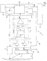
- an optoelectronic distance measurement device is shown overall by 1 and is adapted to measure the distance D of a generic object 2 with respect to this. distance measurement device 1.
- the distance measurement device 1 comprises an optoelectronic light transmission unit, in this case a phototransmitter 3, which is adapted to generate as output, in a predetermined direction and as a function of a control signal CT received as input, a light beam comprising a sequence of light pulses, and an optoelectronic light reception unit, in this case a photoreceiver 4, which is adapted to receive, via an optical triangulation system, the light beam reflected by the object 2 in order to supply as output a first and a second electrical position signal POS 1 , POS 2 , whose values, together, have a correlation with the distance D of the object 2 measured with respect to the distance measurement device 1.
- a phototransmitter 3 which is adapted to generate as output, in a predetermined direction and as a function of a control signal CT received as input, a light beam comprising a sequence of light pulses
- an optoelectronic light reception unit in this case a photoreceiver 4, which is adapted to receive, via
- the distance measurement device 1 further comprises an unbalancing circuit 5 which is connected downstream of the photoreceiver 4 and is adapted to process the first and the second electrical position signal POS 1 , POS 2 supplied by the photoreceiver in order to supply as output a differential signal DIF having a value indicative of the distance D of the object 2, and a processing unit 6 which is adapted to receive and process, as will be described below, the differential signal DIF supplied by the unbalancing circuit 5 in order to determine the distance D of the object 2 with respect to the distance measurement device 1.
- an unbalancing circuit 5 which is connected downstream of the photoreceiver 4 and is adapted to process the first and the second electrical position signal POS 1 , POS 2 supplied by the photoreceiver in order to supply as output a differential signal DIF having a value indicative of the distance D of the object 2, and a processing unit 6 which is adapted to receive and process, as will be described below, the differential signal DIF supplied by the unbalancing circuit 5 in order to determine the distance D of the object 2
- the photoreceiver 4 is advantageously formed by a sensor of known type, generally indicated by the acronym "PSD" (Position Sensitive Device) which has a surface 7 sensitive to the position of the incident light beam and comprises a first and a second output terminal 8, 9.
- PSD Position Sensitive Device
- the photoreceiver 4 is more particularly adapted to supply, to the first and second terminal 8, 9, the first and the second electrical position signal POS 1 , POS 2 , whose values together have a correlation with the position of incidence of the light beam reflected by the object 2 on the surface 7.
- the photoreceiver 4 is more particularly positioned with respect to the phototransmitter 3 so as to provide a precise optical triangulation of the light beam transmitted and received, in this way defining an unequivocal relationship between the position of the point of incidence of the light beam on the surface 7 of the photoreceiver 4 and the distance D of the object 2 measured with respect to the distance measurement device 1.
- This relationship thus provides a correlation between the distance D of the object 2 from the distance measurement device 1 and the values of the first and second position signals POS 1 , POS 2 .
- the unbalancing circuit 5 comprises an amplification stage 10 which may advantageously be formed for instance by a pair of amplification circuits 11 (shown in diagram form) adapted to receive as input the first and the second position signals POS 1 , POS 2 respectively and to supply as output an amplification of these signals, and a regulation stage 12 connected to the photoreceiver 4 via the amplification stage 10 and adapted to unbalance, as a function of a control signal COM received as input, the amplification of the first and/or the second position signal POS 1 , POS 2 .
- amplification stage 10 which may advantageously be formed for instance by a pair of amplification circuits 11 (shown in diagram form) adapted to receive as input the first and the second position signals POS 1 , POS 2 respectively and to supply as output an amplification of these signals
- a regulation stage 12 connected to the photoreceiver 4 via the amplification stage 10 and adapted to unbalance, as a function of a control signal COM received as
- the regulation stage 12 more particularly comprises a variable resistor 13 of known type which may be formed by a digital trimmer whose resistance value R is regulated by means of the control signal COM received as input from the regulation device 12.
- the regulation stage 12 is adapted to vary, as a function of the control signal COM, the resistance R of the variable resistor 13 thereby determining a controlled unbalancing of the amplification of the first and the second position signals POS 1 , POS 2 .
- the unbalancing circuit 5 further comprises a differential stage 14 which is connected downstream of the regulation stage 12 from which it receives the first and second position signals POS 1 , POS 2 , and is adapted to supply as output the differential signal DIF which is determined by the amplification of the difference between the first and the second position signals POS 1 , POS 2 .
- the amplification stage 10 and the regulation stage. 12 define a first and a second amplification "channel" 15, 16 which connect the input terminals of the differential stage 14 to the output terminals of the photoreceiver 4, i.e. they connect the first and the second output terminal 8, 9 of the photoreceiver 4 to a first and respectively a second input terminal 17, 18 of the differential stage 14 and have a respective gain that can be controlled by means of the control signal COM.
- the first and second terminals 17, 18 of the differential stage 14 receive the first and the second position signals POS 1 , POS 2 , appropriately unbalanced by the regulation stage 12, and supply the processing device 6 with the differential signal DIF.
- the processing device 6 comprises a synchronisation unit 19 adapted to generate the control signal CT which controls the transmission of the light pulses by the phototransmitter 3 and a central control unit 20 which is adapted to receive as input the differential signal DIF and to supply as output the signal COM by means of which it regulates the resistance R of the variable resistor 13, and a signal MIS indicating the measurement of the distance D detected.
- the central control unit 20 is more particularly adapted to reach the above-mentioned predetermined circuit condition through a closed loop control in which it carries out, as a function of the value of the differential signal DIF, a variation of the resistance R of the variable resistor 13, which causes a controlled unbalancing of the amplifications present in the two amplification channels 15, 16 and therefore a controlled variation of the first and second position signals POS 1 , POS 2 input with respect to the differential stage 14.
- the central control unit 20 once the above-mentioned predetermined circuit condition has been reached, is able to receive the measurement signal MIS by means of the value of the resistance R of the resistor 13 which caused the above-mentioned predetermined circuit condition to be reached.
- the measurement signal MIS is in particular calculated by means of a circuit function FC(R) stored in a memory (not shown) of the central control unit 20.
- a table containing a plurality of digital values defining the circuit function FC(R) is in particular stored in the memory (not shown), making it possible to obtain, for each value of the resistance R of the resistor 13, the measurement signal MIS indicating the distance D of the object 2.
- the circuit function FC(R) more particularly defines a bi-univocal association between the value of the distance D of the object 2 and the value of the resistance R of the resistor 13 which enables the predetermined circuit condition to be reached.
- the central control unit 20 in addition to carrying out the above-described closed loop control, is adapted to coordinate and control the operations performed by the synchronisation unit 19.
- the distance measurement device 1 further comprises a display unit 22 of known type, for instance a liquid crystal display, which is adapted to receive the measurement signal MIS from the central control unit 20 in order to display the numerical value of the distance of the object 2 detected, calculated with respect to the distance measurement device 1 itself.
- a display unit 22 of known type, for instance a liquid crystal display, which is adapted to receive the measurement signal MIS from the central control unit 20 in order to display the numerical value of the distance of the object 2 detected, calculated with respect to the distance measurement device 1 itself.
- the distance measurement device 1 further comprises a control device 23 of known type, for instance a push button, which is adapted to enable a user to actuate the distance measurement device 1.
- a control device 23 of known type, for instance a push button, which is adapted to enable a user to actuate the distance measurement device 1.
- the control device-23 is in particular connected to the processing unit in order to communicate to the latter an actuation signal encoding a command for the actuation of the distance measurement device 1.
- the distance measurement device 1 is provided with a preliminary search circuit 24 adapted to perform a search for the presence/absence of an object 2 with respect to the distance measurement device 1 before the latter performs the detection of the distance of the object 2.
- a "measurement" operating mode in which the distance measurement device 1 is adapted to perform the above-mentioned control of the resistance R of the resistor 13 in order to reach the predetermined circuit condition in which it is able to supply the measurement signal MIS indicating the distance D of the object 2.
- An “scanning" operating mode in which the distance measurement device 1 is able to perform a preliminary search (described in detail below) in order to detect solely the presence or absence of an object 2 irrespective of the distance D of this object.
- the central control unit is in particular able to select the "scanning" and “measurement” modes of the distance measurement device 1 by controlling, via the selection unit 27, the closure and respectively the opening of the switch 25.
- the distance measurement device 1 controls, via the phototransmitter 3, the transmission of a beam of light pulses.
- the distance measurement device 1 controls, via the selection unit 27, the closure of the switch 25 causing the distance measurement device 1 to pass from the "measurement" operating mode to the "scanning" operating mode in which the preliminary search for the object 2 is actuated.
- the block 100 is followed by the block 110 in which the distance measurement device 1 verifies whether or not an object 2 is present.
- the closure of the switch 25 more particularly causes the exclusion of the first channel 15, i.e. an "imposition" of the predetermined potential V RF (for instance zero) on the first position signal POS 1 in the first input terminal 17 of the differential stage 14; in this condition, the operation of the unbalancing circuit 5 is limited to the amplification of the second channel 16 as the differential signal DIF output from the differential stage 14 corresponds to the difference between the value of the second position signal POS 2 appropriately amplified and the predetermined potential V RF .
- the central control unit 20 is able to establish whether or not an object 2 is present from an analysis of the differential signal DIF.
- the display unit shows the user that no objects 2 are present.
- the block 120 is followed by the block 130 in which the distance measurement is completed and the distance measurement device 1 returns to standby until it receives a new actuation command from the user.
- the position signal POS 2 has a value other than zero as the photoreceiver 4 is excited by the light signal reflected by this object 2.
- the central control unit 20 detects a differential signal DIF of a value other than zero indicating the presence of an object 2.
- the block 110 is followed by the block 140, in which the central control unit 20 commands, by opening the switch 25, transition from the "scanning" operating mode to the "measurement" operating mode.
- the block 140 is followed by the block 150 in which the control unit' 20 detects the value of the differential signal DIF generated, via the reception of a new light pulse converted by the photoreceiver 4 into the respective first and second position signals POS 1 and POS 2 .
- the block 150 is followed by the block 160 in which the central control unit 20 checks the value of the differential signal DIF.
- the block 160 is followed by the block 180.
- the central control unit 20 stores, moreover, the value of the resistance R of the resistor 13 that has determined the new minimum deviation value.
- the minimum deviation value compared in the first check is initially fixed (stored) for instance at a predetermined maximum value.
- the block 170 is followed by the block 190, in which a check is performed on the minimum deviation value stored.
- the block 190 is followed by the block 200 in which the central control unit 20 obtains, via the circuit function FC(R) of the resistance R associated with the stored minimum deviation value, the measurement of the distance D of the object 2 from the distance measurement device 1 and supplies the measurement signal MIS to the display unit 22 via which the distance D of the object 2 is displayed.
- the central control unit 20 in particular varies the resistance R of the resistor 13 according to a binary search algorithm of known type.
- the central control unit 20 is adapted, by means of the binary search algorithm, whenever necessary to determine a precise variation of the resistance R of the resistor 13 as a function of the positive or negative value of the differential signal DIF.
- the binary search algorithm determines the variation of the resistance R of the resistor 13 as a function of the minimum deviation value, so as to reduce the value of the latter to a minimum.
- the distance measurement device 1 has the advantage that it is accurate, i.e. it is able to measure the distance of any object 2 irrespective of the reflective power of that object.
- the distance measurement device 1 has the advantage that it is of simple and economic construction.
- the preliminary search circuit could in particular be omitted from the distance measurement device 1, i.e. it could be able to determine the distance by directly performing the closed loop control without a preliminary check for the presence or absence of the object 2.
Landscapes
- Physics & Mathematics (AREA)
- Engineering & Computer Science (AREA)
- Electromagnetism (AREA)
- Computer Networks & Wireless Communication (AREA)
- General Physics & Mathematics (AREA)
- Radar, Positioning & Navigation (AREA)
- Remote Sensing (AREA)
- Measurement Of Optical Distance (AREA)
- Length Measuring Devices By Optical Means (AREA)
Abstract
An optoelectronic distance measurement device (1)
comprising a light phototransmitter (3) adapted to
transmit a beam of light pulses in a predetermined
direction; a PSD photoreceiver (4) adapted to receive a
beam of light pulses reflected by an object (2) and to
supply as output a first and a second position signal
(PCS1, POS2) indicative of the distance of the object (2)
from the distance measurement device (1); an unbalancing
circuit (5) comprising a resistor (13) having a resistance
(R) variable as a function of a control signal (COM); the
unbalancing circuit (5) being adapted alternatively to
amplify/attenuate the first and the second position signal
(POS1, POS2) by varying the resistance (R) of the variable
resistor as a function of the control signal (COM); a
processing unit (6) adapted to supply as output the
control signal (COM) in order sequentially to vary the
value of the resistance (R) of the resistor (13) until a
predetermined relationship is reached between the first
and the second position signal (POS1, POS2); the
processing unit (6) being adapted to supply as output a
signal (MIS) indicating the distance (D) of the object
(2), obtained as a function of the value of the resistance
(R) of the resistor (13) that has caused the predetermined
relationship between the first and the second position
signals (POS1, POS2) to be reached.
Description
- The present invention relates to an optoelectronic distance measurement device.
- As is known, the optoelectronic distance measurement devices currently known are provided with a phototransmitter adapted to transmit a beam of light pulses in a specific direction for the detection of objects, a photoreceiver of the PSD (Position Sensitive Device) type adapted partially to receive, via an optical triangulation system, the beam of light pulses reflected by an object in order to supply as output a first and a second electrical position signal, whose values together have a correlation with the position of the beam of pulses incident on a surface of the photoreceiver.
- The above-mentioned distance measurement devices are further provided with a processing circuit which receives as input the first and second electrical position signals and is adapted to supply as output a signal calculated as a function of the ratio between the above-mentioned position signals and indicating the distance of the object.
- These distance measurement devices have the drawback that the processing circuit described above is particularly complex with the result that these distance measurement devices have high production costs.
- The object of the present invention is to provide a distance measurement device of the optoelectronic type free from the drawbacks described above.
- The present invention therefore relates to a distance measurement device as described in
claim 1. - The present invention will be described below with reference to the accompanying drawings which show a nonlimiting embodiment thereof and in which:
- Fig. 1 is a diagram of a distance measurement device of the present invention;
- Fig. 2 is a flow diagram relating to the operation of the distance measurement device shown in Fig. 1.
-
- In Fig. 1, an optoelectronic distance measurement device is shown overall by 1 and is adapted to measure the distance D of a generic object 2 with respect to this.
distance measurement device 1. - The
distance measurement device 1 comprises an optoelectronic light transmission unit, in this case aphototransmitter 3, which is adapted to generate as output, in a predetermined direction and as a function of a control signal CT received as input, a light beam comprising a sequence of light pulses, and an optoelectronic light reception unit, in this case aphotoreceiver 4, which is adapted to receive, via an optical triangulation system, the light beam reflected by the object 2 in order to supply as output a first and a second electrical position signal POS1, POS2, whose values, together, have a correlation with the distance D of the object 2 measured with respect to thedistance measurement device 1. - The
distance measurement device 1 further comprises anunbalancing circuit 5 which is connected downstream of thephotoreceiver 4 and is adapted to process the first and the second electrical position signal POS1, POS2 supplied by the photoreceiver in order to supply as output a differential signal DIF having a value indicative of the distance D of the object 2, and aprocessing unit 6 which is adapted to receive and process, as will be described below, the differential signal DIF supplied by theunbalancing circuit 5 in order to determine the distance D of the object 2 with respect to thedistance measurement device 1. - The
photoreceiver 4 is advantageously formed by a sensor of known type, generally indicated by the acronym "PSD" (Position Sensitive Device) which has asurface 7 sensitive to the position of the incident light beam and comprises a first and asecond output terminal 8, 9. - The
photoreceiver 4 is more particularly adapted to supply, to the first andsecond terminal 8, 9, the first and the second electrical position signal POS1, POS2, whose values together have a correlation with the position of incidence of the light beam reflected by the object 2 on thesurface 7. - The
photoreceiver 4 is more particularly positioned with respect to thephototransmitter 3 so as to provide a precise optical triangulation of the light beam transmitted and received, in this way defining an unequivocal relationship between the position of the point of incidence of the light beam on thesurface 7 of thephotoreceiver 4 and the distance D of the object 2 measured with respect to thedistance measurement device 1. - This relationship thus provides a correlation between the distance D of the object 2 from the
distance measurement device 1 and the values of the first and second position signals POS1, POS2. - In Fig. 1, the
unbalancing circuit 5 comprises anamplification stage 10 which may advantageously be formed for instance by a pair of amplification circuits 11 (shown in diagram form) adapted to receive as input the first and the second position signals POS1, POS2 respectively and to supply as output an amplification of these signals, and aregulation stage 12 connected to thephotoreceiver 4 via theamplification stage 10 and adapted to unbalance, as a function of a control signal COM received as input, the amplification of the first and/or the second position signal POS1, POS2. - The
regulation stage 12 more particularly comprises avariable resistor 13 of known type which may be formed by a digital trimmer whose resistance value R is regulated by means of the control signal COM received as input from theregulation device 12. - In other words, the
regulation stage 12 is adapted to vary, as a function of the control signal COM, the resistance R of thevariable resistor 13 thereby determining a controlled unbalancing of the amplification of the first and the second position signals POS1, POS2. - The
unbalancing circuit 5 further comprises adifferential stage 14 which is connected downstream of theregulation stage 12 from which it receives the first and second position signals POS1, POS2, and is adapted to supply as output the differential signal DIF which is determined by the amplification of the difference between the first and the second position signals POS1, POS2. - It will be appreciated from the above description that the
amplification stage 10 and the regulation stage. 12 define a first and a second amplification "channel" 15, 16 which connect the input terminals of thedifferential stage 14 to the output terminals of thephotoreceiver 4, i.e. they connect the first and thesecond output terminal 8, 9 of thephotoreceiver 4 to a first and respectively a second input terminal 17, 18 of thedifferential stage 14 and have a respective gain that can be controlled by means of the control signal COM. - The first and second terminals 17, 18 of the
differential stage 14 receive the first and the second position signals POS1, POS2, appropriately unbalanced by theregulation stage 12, and supply theprocessing device 6 with the differential signal DIF. - The
processing device 6 comprises asynchronisation unit 19 adapted to generate the control signal CT which controls the transmission of the light pulses by thephototransmitter 3 and acentral control unit 20 which is adapted to receive as input the differential signal DIF and to supply as output the signal COM by means of which it regulates the resistance R of thevariable resistor 13, and a signal MIS indicating the measurement of the distance D detected. - The
central control unit 20 is more particularly able to supply as output the measurement signal MIS when a predetermined circuit conditions occurs, which is satisfied when the differential signal DIF has a predetermined value DIFo, for instance a voltage and/or current value substantially equal to zero (DIF=DIFo=0). - The
central control unit 20 is more particularly adapted to reach the above-mentioned predetermined circuit condition through a closed loop control in which it carries out, as a function of the value of the differential signal DIF, a variation of the resistance R of thevariable resistor 13, which causes a controlled unbalancing of the amplifications present in the twoamplification channels differential stage 14. - The
central control unit 20, once the above-mentioned predetermined circuit condition has been reached, is able to receive the measurement signal MIS by means of the value of the resistance R of theresistor 13 which caused the above-mentioned predetermined circuit condition to be reached. - The measurement signal MIS is in particular calculated by means of a circuit function FC(R) stored in a memory (not shown) of the
central control unit 20. - A table containing a plurality of digital values defining the circuit function FC(R) is in particular stored in the memory (not shown), making it possible to obtain, for each value of the resistance R of the
resistor 13, the measurement signal MIS indicating the distance D of the object 2. - The circuit function FC(R) more particularly defines a bi-univocal association between the value of the distance D of the object 2 and the value of the resistance R of the
resistor 13 which enables the predetermined circuit condition to be reached. - The
central control unit 20, in addition to carrying out the above-described closed loop control, is adapted to coordinate and control the operations performed by thesynchronisation unit 19. - With reference to Fig. 1, the
distance measurement device 1 further comprises a display unit 22 of known type, for instance a liquid crystal display, which is adapted to receive the measurement signal MIS from thecentral control unit 20 in order to display the numerical value of the distance of the object 2 detected, calculated with respect to thedistance measurement device 1 itself. - Preferably, but not 'necessarily, the
distance measurement device 1 further comprises acontrol device 23 of known type, for instance a push button, which is adapted to enable a user to actuate thedistance measurement device 1. - The control device-23 is in particular connected to the processing unit in order to communicate to the latter an actuation signal encoding a command for the actuation of the
distance measurement device 1. - Preferably, but not necessarily, the
distance measurement device 1 is provided with apreliminary search circuit 24 adapted to perform a search for the presence/absence of an object 2 with respect to thedistance measurement device 1 before the latter performs the detection of the distance of the object 2. - The
preliminary search circuit 24 in particular comprises aswitch 25 which is connected between thefirst output terminal 8 of thephotoreceiver 4 and aterminal 26 having a predetermined potential VRF (for instance an earth potential VRF=0) and aselection unit 27 which cooperates with thecentral control unit 20 and is adapted selectively to control the opening/closure of theswitch 25 thereby determining the selection of one of the following modes of operation of thedistance measurement device 1. - A "measurement" operating mode, in which the
distance measurement device 1 is adapted to perform the above-mentioned control of the resistance R of theresistor 13 in order to reach the predetermined circuit condition in which it is able to supply the measurement signal MIS indicating the distance D of the object 2. - An "scanning" operating mode, in which the
distance measurement device 1 is able to perform a preliminary search (described in detail below) in order to detect solely the presence or absence of an object 2 irrespective of the distance D of this object. - The central control unit is in particular able to select the "scanning" and "measurement" modes of the
distance measurement device 1 by controlling, via theselection unit 27, the closure and respectively the opening of theswitch 25. - The operation of the
distance measurement device 1 will now be described with reference to Fig. 2. - It is assumed initially that the
distance measurement device 1 is provided with thepreliminary search circuit 24, that it is operational, i.e. has been actuated by a user via thecontrol device 23, that the predetermined value DIFo for the achievement of the predetermined circuit condition is substantially equal to zero (DIFo=0) and that thedistance measurement device 1 is in the "measurement" operating mode, i.e. theswitch 25 is open. - In the
initial block 100, thedistance measurement device 1 controls, via thephototransmitter 3, the transmission of a beam of light pulses. - In the
block 100, thedistance measurement device 1 controls, via theselection unit 27, the closure of theswitch 25 causing thedistance measurement device 1 to pass from the "measurement" operating mode to the "scanning" operating mode in which the preliminary search for the object 2 is actuated. - The
block 100 is followed by theblock 110 in which thedistance measurement device 1 verifies whether or not an object 2 is present. - In the "scanning" operating mode, the closure of the
switch 25 more particularly causes the exclusion of thefirst channel 15, i.e. an "imposition" of the predetermined potential VRF (for instance zero) on the first position signal POS1 in the first input terminal 17 of thedifferential stage 14; in this condition, the operation of theunbalancing circuit 5 is limited to the amplification of thesecond channel 16 as the differential signal DIF output from thedifferential stage 14 corresponds to the difference between the value of the second position signal POS2 appropriately amplified and the predetermined potential VRF. - In this operating condition, the
central control unit 20 is able to establish whether or not an object 2 is present from an analysis of the differential signal DIF. - If no object 2 is present, the position signal POS2 is obviously zero, as the
photoreceiver 4 is not excited by light signals. In this case, thecentral control unit 20 detects a differential signal DIF=0 and theblock 110 is followed by theblock 120, in which thecentral control unit 20 assigns an infinite value to the distance D, encoded by the measurement signal MIS. In this case, the display unit shows the user that no objects 2 are present. - The
block 120 is followed by theblock 130 in which the distance measurement is completed and thedistance measurement device 1 returns to standby until it receives a new actuation command from the user. - In the opposite case, i.e. when an object 2 is present, the position signal POS2 has a value other than zero as the
photoreceiver 4 is excited by the light signal reflected by this object 2. In this case thecentral control unit 20 detects a differential signal DIF of a value other than zero indicating the presence of an object 2. - In this condition, the
block 110 is followed by theblock 140, in which thecentral control unit 20 commands, by opening theswitch 25, transition from the "scanning" operating mode to the "measurement" operating mode. - In the
block 140, thecentral control unit 20 initialises a counter CONT=1 and controls, by means of the control signal COM, a first variation of the resistance R of theresistor 13, assigning them a predetermined initial value Ro for instance equal to the maximum or minimum value of thisresistor 13. - The
block 140 is followed by theblock 150 in which the control unit' 20 detects the value of the differential signal DIF generated, via the reception of a new light pulse converted by thephotoreceiver 4 into the respective first and second position signals POS1 and POS2. - The
block 150 is followed by theblock 160 in which thecentral control unit 20 checks the value of the differential signal DIF. - If the difference between the value of the differential signal DIF detected and the value of the differential signal DIF that satisfies the predetermined circuit condition (DIF=0) is greater than a minimum deviation value, the
block 160 is followed by theblock 180. - If, however, the difference between the value of the differential signal DIF detected, and the value of the differential signal DIF that satisfies the predetermined circuit condition (DIF=0) is lower than the minimum deviation value, the
block 160 is followed by theblock 170 in which thecentral control unit 20 updates the minimum deviation value by assigning it a new value which is obtained from the difference between the value of the differential signal DIF detected, and the value of the differential signal DIF indicating the predetermined circuit condition (DIF=0). - In the
block 170, thecentral control unit 20 stores, moreover, the value of the resistance R of theresistor 13 that has determined the new minimum deviation value. - It will be appreciated from the above description that the minimum deviation value compared in the first check (first cycle in which the
block 160 is involved) is initially fixed (stored) for instance at a predetermined maximum value. - The
block 170 is followed by theblock 190, in which a check is performed on the minimum deviation value stored. - If the stored minimum deviation value is substantially equal to zero (occurrence of the predetermined condition, i.e. the value of the differential signal DIF is substantially equal to zero), the
block 190 is followed by theblock 200 in which thecentral control unit 20 obtains, via the circuit function FC(R) of the resistance R associated with the stored minimum deviation value, the measurement of the distance D of the object 2 from thedistance measurement device 1 and supplies the measurement signal MIS to the display unit 22 via which the distance D of the object 2 is displayed. - If, however, the stored minimum deviation value is other than zero, the
block 190 is followed by theblock 180 in which it is checked whether the counter CONT has reached a maximum value NMAX, i.e. if the relationship CONT<=NMAX has occurred. - If not, i.e. if CONT>NMAX, the
block 180 is followed by theblock 200 described above and, if so, i.e. if CONT<=NMAX, theblock 180 is followed by theblock 210 in which thecentral control unit 20 causes, via the control signal COM, a new variation of the value of the resistance R of theresistor 13. - The
central control unit 20 in particular varies the resistance R of theresistor 13 according to a binary search algorithm of known type. - The
central control unit 20 is adapted, by means of the binary search algorithm, whenever necessary to determine a precise variation of the resistance R of theresistor 13 as a function of the positive or negative value of the differential signal DIF. - In other words, the binary search algorithm determines the variation of the resistance R of the
resistor 13 as a function of the minimum deviation value, so as to reduce the value of the latter to a minimum. - The
block 210 is followed by theblock 150, in which thecentral control unit 20 again performs the cycle to detect the differential signal DIF, which is subsequently processed in theblock 160 in which the stored minimum deviation value is compared with the difference between the value of the differential signal DIF detected and the value of the differential signal DIF associated with the predetermined circuit condition (DIF=0). - The
distance measurement device 1 has the advantage that it is accurate, i.e. it is able to measure the distance of any object 2 irrespective of the reflective power of that object. - Lastly, the
distance measurement device 1 has the advantage that it is of simple and economic construction. - It will be appreciated that modifications and variations may be made to the
distance measurement device 1 as described and illustrated without thereby departing from the scope of the present invention. - The preliminary search circuit could in particular be omitted from the
distance measurement device 1, i.e. it could be able to determine the distance by directly performing the closed loop control without a preliminary check for the presence or absence of the object 2.
Claims (16)
- An optoelectronic distance measurement device (1) characterised in that it comprises:light transmission means (3) adapted to transmit a beam of light pulses in a predetermined direction;

- An optoelectronic distance measurement device as claimed in claim 1, characterised in that the unbalancing means (5) comprise resistor means (13) having a variable resistive circuit parameter (R) whose value is controlled by the processing means (6) by means of the control signal (COM).
- An optoelectronic distance measurement device as claimed in any one of the preceding claims, characterised in that the unbalancing means (5) comprise differential means (14) receiving as input the first and the second position signals (POS1, POS2) and adapted to process these first and second position signals (POS1, POS2) in order to supply to the processing means (6) a differential signal (DIF) defined by the difference between the first and second position signal (POS1, POS2).
- An optoelectronic distance measurement device as claimed in claim 3, characterised in that the predetermined relationship is defined by the condition in which the differential signal (DIF) received as input from the processing means (6) has a value substantially equal to a predetermined value.
- An optoelectronic distance measurement device as claimed in claim 3, characterised in that the predetermined relationship is defined by the condition in which the value of the differential signal (DIF) received as input from the processing means (6) is substantially equal to zero.
- An optoelectronic distance measurement device as claimed in any one of the preceding claims, characterised in that the unbalancing means (5) comprise a first and a second amplification channel (15, 16).
- An optoelectronic distance measurement device as claimed in claim 6, characterised in that it comprises preliminary search means (24) controlled by the processing means (6) and adapted to cancel out the contribution of the first or second amplification channel (15, 16) in order to enable the processing means (6) to process one of the two position signals (POS1, POS2) and solely to detect the presence or absence of an object (2).
- An optoelectronic distance measurement device as claimed in claim 7, characterised in that the processing means (6) comprise first checking means (110) adapted, to detect the presence or absence of an object (2).
- An optoelectronic distance measurement device as claimed in claim 8, characterised in that the processing means (6) comprise second checking means (190) adapted to check whether the predetermined condition has occurred.
- An optoelectronic distance measurement device as claimed in any one of claims 2 to 9, characterised in that the processing means (6) comprise means (200) for calculating the distance (D) adapted to supply as output the measurement signal (MIS) determined as a function of the resistance (R) of the resistor means (13) which determines the predetermined condition.
- An optoelectronic distance measurement device as claimed in any one of claims 2 to 10, characterised in 'that the processing means (6) are adapted to vary the resistance (R) of the resistor means (13) by means of a binary search algorithm.
- An optoelectronic distance measurement device as claimed in any one of claims 2 to 11, characterised in that the unbalancing means (5) comprise amplification means (11).
- An optoelectronic distance measurement device as claimed in any one of the preceding claims, characterised in that it comprises display means (22) receiving as input the measurement signal (MIS) in order to display the distance (D) of the object (2).
- An optoelectronic distance measurement device as claimed in any one of claims 2 to 13, characterised in that the resistor means (13) are formed by a digital trimmer.
- An optoelectronic distance measurement device as claimed in any one of the preceding claims, characterised in that the processing means (6) comprise synchronisation means (19) adapted to supply a synchronisation signal (CT) to the light transmission means (3) in order to command the transmission of the light beam.
- An optoelectronic distance measurement device as claimed in any one of the preceding claims, characterised in that the optoelectronic reception means (4) are PSD photoreceivers.
Applications Claiming Priority (2)
| Application Number | Priority Date | Filing Date | Title |
|---|---|---|---|
| ITBO010114 | 2001-03-02 | ||
| IT2001BO000114A ITBO20010114A1 (en) | 2001-03-02 | 2001-03-02 | OPTOELECTRONIC DISTANCE METER DEVICE |
Publications (1)
| Publication Number | Publication Date |
|---|---|
| EP1237011A1 true EP1237011A1 (en) | 2002-09-04 |
Family
ID=11439160
Family Applications (1)
| Application Number | Title | Priority Date | Filing Date |
|---|---|---|---|
| EP02004695A Withdrawn EP1237011A1 (en) | 2001-03-02 | 2002-02-28 | Optoelectronic distance measurement device |
Country Status (2)
| Country | Link |
|---|---|
| EP (1) | EP1237011A1 (en) |
| IT (1) | ITBO20010114A1 (en) |
Citations (4)
| Publication number | Priority date | Publication date | Assignee | Title |
|---|---|---|---|---|
| US5225689A (en) * | 1990-12-15 | 1993-07-06 | Leuze Electronic Gmbh & Co. | Reflected light sensor having dual emitters and receivers |
| DE4311691A1 (en) * | 1993-04-08 | 1994-10-13 | Sick Erwin Gmbh | Method for adjusting an optical distance (clearance) probe |
| US5923427A (en) * | 1997-07-10 | 1999-07-13 | Banner Engineering Corporation | Optical triangulation distance sensing system and method using a position sensitive detector and an automatic power controlled light source |
| DE19917487A1 (en) * | 1998-04-22 | 1999-11-11 | Leuze Electronic Gmbh & Co | Optoelectronic device for detecting objects in monitored space |
-
2001
- 2001-03-02 IT IT2001BO000114A patent/ITBO20010114A1/en unknown
-
2002
- 2002-02-28 EP EP02004695A patent/EP1237011A1/en not_active Withdrawn
Patent Citations (4)
| Publication number | Priority date | Publication date | Assignee | Title |
|---|---|---|---|---|
| US5225689A (en) * | 1990-12-15 | 1993-07-06 | Leuze Electronic Gmbh & Co. | Reflected light sensor having dual emitters and receivers |
| DE4311691A1 (en) * | 1993-04-08 | 1994-10-13 | Sick Erwin Gmbh | Method for adjusting an optical distance (clearance) probe |
| US5923427A (en) * | 1997-07-10 | 1999-07-13 | Banner Engineering Corporation | Optical triangulation distance sensing system and method using a position sensitive detector and an automatic power controlled light source |
| DE19917487A1 (en) * | 1998-04-22 | 1999-11-11 | Leuze Electronic Gmbh & Co | Optoelectronic device for detecting objects in monitored space |
Also Published As
| Publication number | Publication date |
|---|---|
| ITBO20010114A1 (en) | 2002-09-02 |
| ITBO20010114A0 (en) | 2001-03-02 |
Similar Documents
| Publication | Publication Date | Title |
|---|---|---|
| CA1258691A (en) | Remotely calibratable instrument system | |
| US6897777B2 (en) | Non-linear junction detector | |
| US6124936A (en) | Color discrimination system | |
| JPS633269B2 (en) | ||
| JP2010156711A (en) | Device and method for distance measurement | |
| US4849754A (en) | Remotely calibratable instrument system | |
| EP1237011A1 (en) | Optoelectronic distance measurement device | |
| EP1209487B1 (en) | Method and device for detection of an object, with background elimination | |
| JP2006078371A (en) | Ranging sensor and setting method therefor | |
| CA1301859C (en) | Automatic gain control circuit | |
| JP2551732B2 (en) | Optoelectronic control unit and optimum gain automatic setting method thereof | |
| GB2218214A (en) | Remotely calibratable instrument system | |
| US7106422B2 (en) | Rangefinder and measuring method | |
| US20220345564A1 (en) | Portable control apparatus for controlling a motion sensor | |
| JP2958371B2 (en) | Device for adjusting operating condition of photoelectric sensor and method for adjusting operating condition thereof | |
| JP2004215315A (en) | Photoelectric sensor and its sensitivity setting method | |
| KR102208923B1 (en) | Beacon signal reliability verification method and system | |
| JPH09167952A (en) | Photoelectric switch | |
| JPH0480566B2 (en) | ||
| CN106030338A (en) | Method for operating an optical proximity switch according to the light-travel time principle | |
| JPH06342069A (en) | Laser range finder | |
| JPH05206820A (en) | Method and device for controlling sensitivity of photoelectric switch | |
| WO2025123126A3 (en) | Characterizing integrated circuit devices using a vapor cell sensor | |
| JPH08287798A (en) | Photoelectric switch control method | |
| JPS63236985A (en) | Ultrasonic distance measuring device |
Legal Events
| Date | Code | Title | Description |
|---|---|---|---|
| PUAI | Public reference made under article 153(3) epc to a published international application that has entered the european phase |
Free format text: ORIGINAL CODE: 0009012 |
|
| AK | Designated contracting states |
Kind code of ref document: A1 Designated state(s): AT BE CH CY DE DK ES FI FR GB GR IE IT LI LU MC NL PT SE TR |
|
| AX | Request for extension of the european patent |
Free format text: AL;LT;LV;MK;RO;SI |
|
| 17P | Request for examination filed |
Effective date: 20030303 |
|
| AKX | Designation fees paid |
Designated state(s): DE ES FR GB IT |
|
| 17Q | First examination report despatched |
Effective date: 20070105 |
|
| STAA | Information on the status of an ep patent application or granted ep patent |
Free format text: STATUS: THE APPLICATION IS DEEMED TO BE WITHDRAWN |
|
| 18D | Application deemed to be withdrawn |
Effective date: 20090901 |