EP1235278A2 - Heterojunction bipolar transistor (HBT) having an improved emitter-base junction - Google Patents
Heterojunction bipolar transistor (HBT) having an improved emitter-base junction Download PDFInfo
- Publication number
- EP1235278A2 EP1235278A2 EP01124893A EP01124893A EP1235278A2 EP 1235278 A2 EP1235278 A2 EP 1235278A2 EP 01124893 A EP01124893 A EP 01124893A EP 01124893 A EP01124893 A EP 01124893A EP 1235278 A2 EP1235278 A2 EP 1235278A2
- Authority
- EP
- European Patent Office
- Prior art keywords
- emitter
- base
- inp
- intermediate layer
- gaassb
- Prior art date
- Legal status (The legal status is an assumption and is not a legal conclusion. Google has not performed a legal analysis and makes no representation as to the accuracy of the status listed.)
- Ceased
Links
Images




Classifications
-
- H—ELECTRICITY
- H10—SEMICONDUCTOR DEVICES; ELECTRIC SOLID-STATE DEVICES NOT OTHERWISE PROVIDED FOR
- H10D—INORGANIC ELECTRIC SEMICONDUCTOR DEVICES
- H10D10/00—Bipolar junction transistors [BJT]
- H10D10/80—Heterojunction BJTs
- H10D10/821—Vertical heterojunction BJTs
-
- H—ELECTRICITY
- H10—SEMICONDUCTOR DEVICES; ELECTRIC SOLID-STATE DEVICES NOT OTHERWISE PROVIDED FOR
- H10D—INORGANIC ELECTRIC SEMICONDUCTOR DEVICES
- H10D62/00—Semiconductor bodies, or regions thereof, of devices having potential barriers
- H10D62/10—Shapes, relative sizes or dispositions of the regions of the semiconductor bodies; Shapes of the semiconductor bodies
- H10D62/13—Semiconductor regions connected to electrodes carrying current to be rectified, amplified or switched, e.g. source or drain regions
- H10D62/133—Emitter regions of BJTs
- H10D62/136—Emitter regions of BJTs of heterojunction BJTs
Definitions
- the present invention relates generally to transistors, and, more particularly, to a heterojunction bipolar transistor (HBT) having an improved emitter-base junction.
- HBT heterojunction bipolar transistor
- Heterojunction bipolar transistors have become state of the art, particularly in npn form, for applications in which high switching speeds and high frequency operation are desired.
- the emitter in an HBT has a bandgap wider than the bandgap of the base, thus creating an energy barrier in the valence band at the emitter-base junction that inhibits the unwanted flow of holes from the base region to the emitter region. This arrangement increases the emitter injection efficiency, current gain and operating frequency of the HBT.
- First generation commercial HBTs were based on a gallium-arsenide (GaAs) substrate and semiconductor materials lattice matched to GaAs.
- Next generation HBTs are likely to be based on an indium-phosphide (InP) substrate and semiconductor materials lattice matched to InP.
- the base of such an HBT is fabricated from either the indium-gallium-arsenide (InGaAs) material system or the gallium-arsenide-antimonide (GaAsSb) material system, with the collector and the emitter fabricated from, for example, InP, aluminum-indium-arsenide (AlInAs) or InGaAs.
- HBTs that are fabricated using GaAsSb as the base material and AlInAs as the emitter material offer certain advantages over HBTs in which the base material is GaAsSb and the emitter is material is InP.
- the conduction band energy line-up between AlInAs and GaAsSb (emitter-base) provides certain advantages, such as higher current-density operation, and hence higher frequency operation.
- HBTs lattice-matched to InP but with a base layer different from GaAsSb fail to offer these advantages.
- the use of the same structure but with an InGaAs base has the large valence-band discontinuity ⁇ E v at the metallurgical base and the benefit of the wide-bandgap InP, but presents a barrier to electron collection, which could result in undesirable stored charge in the base. This compromises the frequency response and maximum current of the device.
- Any scheme to eliminate this barrier compromises the desired features of the large valence-band discontinuity ⁇ E V at the metallurgical collector-base junction, and the benefit of the wide-bandgap InP.
- the type II band lineup leads to two undesirable features. Both are related to the discontinuity in the electron concentration across the heterojunction of exp (-q ⁇ E c /kT), where q is the electron charge, ⁇ E c is the conduction band discontinuity, k is Boltzmann's constant, and T is the absolute junction temperature. Since ⁇ E C is approximately 0.18 ⁇ 0.1 eV, the ratio of electron concentration across the discontinuity is in the range of 2 x 10 -5 to 5 x 10 -2 at room temperature.
- the interface current density j interface qn emitter v interface , where n emitter is the electron density on the emitter side of the interface and where v interface is the interface recombination velocity.
- the interface recombination velocity v interface ⁇ n v thermal N traps + K s_i_rad p base , where ⁇ n is the cross-section for capture of an electron by an interface trap, v thermal is the thermal velocity of electrons, N traps is the trap concentration as a density per unit area, K s_i_rad is a constant that describes the proportionality of spatially indirect radiative recombination at the interface, and p base is the hole concentration on the base side of the interface.
- Spatially indirect recombination is band-to-band recombination between electrons that are localized on one side of a type-II heterojunction (in this example the InP side) and holes that are localized on the other side (in this example the GaAsSb side).
- the recombination is referred to as spatially indirect because the electrons and holes are separated according to classical physics. According to quantum physics the electrons and holes are not perfectly localized. They are represented by wave functions that slightly overlap. Therefore, some recombination occurs. Both of these effects are known to those having ordinary skill in the art.
- the injection current density j injection qn base v base , where n base is the injected electron concentration on the base side of the emitter-base junction and where v base is the electron velocity through the base.
- the ratio j injection / j interface v base n base /v interface n emitter represents an upper limit to the current gain of the transistor.
- the ratio of electron density on either side of the metallurgical junction leads to an effective multiplication of the interface recombination velocity by exp (q ⁇ E c /kT), directly affecting the current gain.
- the emitter capacitance becomes quite large and the frequency response is rapidly lowered.
- the electron velocity through the base denoted by v base
- v base the electron velocity through the base
- the experimental values are closer to the high end of this range, but still seriously limit the device operation by limiting the emitter charging frequency g m /(2 ⁇ C e ), where g m is the dynamic emitter conductance and C e is the emitter junction capacitance.
- FIG. 1 is a graphical illustration showing an energy band diagram of a conventional InP emitter/GaAsSb base/InP collector HBT under modest forward electrical bias on the emitter-base junction.
- FIG. 2 is a graphical illustration showing an energy band diagram of the InP emitter/GaAsSb base/InP collector HBT of FIG. 1 at a strong forward bias on the emitter-base junction.
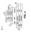
- FIG. 3 is a cross-sectional view illustrating an HBT constructed in accordance with the invention.
- FIG. 6 is a cross-sectional view illustrating an alternative embodiment of the HBT of FIG. 3.
- HBT npn heterojunction bipolar transistor
- a heavily p-doped GaAsSb base layer 108 is grown over the InP collector layer 104 and metal contacts 112 are applied to portions of the base layer 108 as shown.
- an intermediate layer 110 is grown on the base layer 108.
- the thin intermediate layer 110 forms a narrow quantum well at the emitter-base junction.
- the intermediate layer 110 has a lattice constant that conforms to the lattice constant of the GaAsSb base layer 108 and the AlInAs emitter 114.
- the intermediate layer 110 can be grown lattice-matched to the GaAsSb base layer 108 and the AlInAs emitter 114 using, for example, InP.
- the bulk lattice constant of the intermediate layer 110 matches the lattice constant of the GaAsSb base material and the AlInAs emitter material.
- the intermediate layer 110 can be made of a non lattice-matched material, but made sufficiently thin and grown pseudomorphically so that its lattice parameter conforms to the lattice parameter of the GaAsSb base layer 108 and the AlInAs emitter 114.
- the intermediate layer 110 constructed using In X Ga 1-X P, where X approaches, but does not equal 1, the intermediate layer 110 would be pseudomorphic and have a lattice constant that conforms to the lattice constant of the GaAsSb base layer 108 and the AlInAs emitter 114.
- a thin intermediate layer When a thin intermediate layer is grown pseudomorphically it becomes "strained” so that its lattice constant conforms to the lattice constant of the substrate material.
- the lattice constant in a pseudomorphic layer is stretched or compressed so that it matches the substrate lattice in the two dimensions perpendicular to the growth direction.
- the lattice parameter in the growth direction will be completely different, the lattice constant presented by the pseudomorphic surface to incoming constituent atoms during growth is the same as a lattice-matched surface. Therefore, physically, the use of a thin pseudomorphic layer as the intermediate layer 110 is very similar to the use of a perfectly lattice-matched intermediate layer 110.
- the intermediate layer 110 is formed using InP.
- other materials having a bulk lattice constant that matches the lattice constant of the GaAsSb base material and the AlInAs emitter material may be used to form the intermediate layer 110.
- pseudomorphically grown intermediate layers other than In X Ga 1-X P, where X approaches, but does not equal 1 may be used.
- the emitter 114 comprises a lightly n-doped AlInAs layer 116 grown over the intermediate layer 110.
- a heavier n-doped AlInAs layer 118 is grown over the AlInAs layer 116, and a heavily n-doped InGaAs layer 120 is grown over the AlInAs layer 118.
- These two layers 118 and 120 provide an ohmic contact to the emitter 114 to allow metal contact 122 to be applied over the emitter 114.
- the subcollector layer 102, collector layer 104, base layer 108, intermediate layer 110 and the emitter 114 can be grown using, for example but not limited to, molecular beam epitaxy (MBE).
- MBE molecular beam epitaxy
- the velocity of interface recombination depends in part on the number of traps, N traps , present at the metallurgical emitter-base junction.
- N traps present at the metallurgical emitter-base junction.
- the InP/GaAsSb heterojunction formed by the GaAsSb base layer 108 and the intermediate layer 110 appears to have an acceptably low density of traps since HBT's with good gain can be grown in this material system. This is difficult to achieve with an AlInAs/GaAsSb junction.
- the structure formed using an intermediate layer 110 of InP behaves as if it has the desirable band lineup of the AlInAs/GaAsSb emitter-base structure, while exhibiting the low density of traps characteristic of the InP/GaAsSb emitter-base structure. This is accomplished by exploiting the quantum nature, and light effective mass, of the conduction electrons in most type III-V compounds, and in InP in particular, and the localized nature of interface traps. The result is a structure that can be grown easily and that has the desirable electron-transport features of the AlInAs/GaAsSb/InP HBT with current gain equal to or better than the InP/GaAsSb/InP HBT.
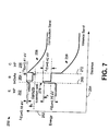
- FIG. 4 is a graphical illustration showing an energy band diagram 150 of the HBT of FIG. 3.
- the InP quantum well 178 forms two heterojunctions between the AlInAs emitter region 162 and the GaAsSb base region 164. One heterojunction is formed at the InP/GaAsSb interface 168 and one heterojunction is formed at the InP/AlInAs interface 188.
- This effective heterojunction is at the InP/GaAsSb interface 168 in the valence band, but is at the AlInAs/InP interface 188 in the conduction band.
- the heterojunction formed at the GaAsSb/InP interface 172 between the GaAsSb base region 164 and the InP collector region 166 provides a conduction band discontinuity ⁇ E c of 0.18 eV and a valence band discontinuity ⁇ E v of 0.76 eV.
- the desirable properties for an AlInAs/GaAsSb HBT stem from the band lineup of these materials.
- band lineup is thought to be independent of any interposed layers.
- the placement of the InP intermediate layer 110 between the GaAsSb base layer 108 and the AlInAs emitter 114 should not materially affect the band lineup between the AlInAs emitter region 162 and the GaAsSb base region 164.
- the InP intermediate layer 110 creates an InP quantum well 178 at the metallurgical junction between the AlInAs emitter region 162 and the GaAsSb region 164. If electrons are captured in this well, they will tend to contribute to the undesirable emitter recombination current.
- the InP quantum well 178 can be designed to have virtually no effect on the electron density. In effect, the InP quantum well 178 can be designed to be electrically transparent, as will be described below.
- FIG. 5 is a graphical illustration 190 of the sub-band energy of an InP quantum well.
- the vertical axis represents sub-band energy in eV and the horizontal axis represents the width of the quantum well in nm.
- the trace 192 illustrates the calculated eigenenergy of the lowest energy state in an asymmetric square-well potential, with a 0.18 eV barrier on one side and a 0.25 eV barrier on the other.
- the electron is assumed to have an effective mass of 0.077 m o , where m o is the free electron mass.
- the energy of the lowest state is so close to the band energy of the GaAsSb base that thermal smearing of the electron energy will render any excess in the electron population negligibly small.
- a quantum well that confines the electrons in the direction perpendicular to the interface, and leaves them free in the other 2 dimensions with a single sub-band has a constant density of states N ss of about 3.2 ⁇ 10 13 cm -2 eV -1 for an effective mass of 0.077 m o .
- the intermediate layer is electrically transparent in that it has no effect on the electron density and it does not present any barrier to electron transport.
- a thin InP intermediate layer between the AlInAs emitter and the GaAsSb base provides a lattice matched surface to both the AlInAs emitter and the GaAsSb base and also allows the HBT to retain the superior performance accorded by the use of the AlInAs emitter.
- the lattice match between the GaAsSb base and the InP quantum well and the lattice match between the InP quantum well and the AlInAs emitter can be achieved either through direct lattice match, or by pseudomorphically growing a thin layer of a non lattice-matched material as the intermediate layer.
- inserting an InP intermediate layer 110 between the emitter 114 and the base layer 108 has little or no harmful effect on the gain, but there is also an additional, positive, attribute.
- the AlInAs/GaAsSb interface is replaced with AlInAs/InP and InP/GaAsSb interfaces.
- the use of an AlInAs emitter, or any emitter having a conduction band energy larger than or equal to the conduction band energy in the base eliminates spatially indirect band-to-band recombination. This remains true for the emitter with a thin InP intermediate layer since, as discussed above, there is no bound state for such a thin InP layer.
- the key interface for determining the interface recombination velocity is the InP/GaAsSb interface 168.
- the heterojunction formed at this interface 168 can be grown with good properties and experimental results support the superiority of the InP/GaAsSb interface over the AlInAs/GaAsSb interface. Further, the combination of the AlInAs/InP and InP/GaAsSb interfaces exhibits better current gain than the AlInAs/GaAsSb interface alone.
- a p-doped InGaAs base layer 208 is grown over the InP collector layer 204 and metal contacts 212 are applied to portions of the base layer 208 as shown.
- an intermediate layer 210 of GaAsSb is grown on the InGaAs base layer 208.
- the thin GaAsSb intermediate layer 210 forms a narrow quantum well at the emitter-base junction, but in this embodiment, the quantum well is formed in the valence band instead of in the conduction band.
- the intermediate layer 210 of GaAsSb has a lattice constant that conforms to the lattice constant of the InGaAs base layer 208 and the InP emitter 214.
- the intermediate layer 210 can be grown lattice-matched to the InGaAs base layer 208 and the InP emitter 214 by using a material such as GaAsSb.
- the intermediate layer 210 can be made of a non lattice-matched material, but made sufficiently thin and grown pseudomorphically so that its lattice parameter conforms to the lattice parameter of the InGaAs base layer 208 and the InP emitter 214.
- such a thin intermediate layer can be grown pseudomorphically and "strained" so that it conforms to the substrate material's lattice constant.
- the emitter 214 comprises a lightly n-doped InP layer 216 grown over the intermediate layer 210 comprising GaAsSb. A heavier n-doped InP layer 218 is grown over the InP layer 216, and a heavily n-doped InGaAs layer 220 is grown over the InP layer 218. These two layers 218 and 220 provide an ohmic contact to the emitter 214 to allow metal contact 222 to be applied over the emitter 214.
- the subcollector layer 202, collector layer 204, base layer 208, intermediate layer 210 and the emitter 214 can be grown using, for example but not limited to, molecular beam epitaxy (MBE).
- MBE molecular beam epitaxy
- this effective heterojunction is at the InP/GaAsSb interface 268 in the valence band, but is at the GaAsSb/ InGaAs interface 288 in the conduction band.
- an asymmetrical quantum well 278 is formed in the valence band at the emitter-base junction as a result of the GaAsSb intermediate layer 210 formed between the InP emitter 214 and the InGaAs base layer 208 of FIG. 6.
Landscapes
- Bipolar Transistors (AREA)
- Recrystallisation Techniques (AREA)
Abstract
Description
Claims (10)
- A heterojunction bipolar transistor (HBT) (100), comprising:a collector (104);a base (108) located over the collector (104); andan emitter (114) located over the base (108), the emitter (114) including an intermediate layer (110) in contact with the base (108), the intermediate layer (110) being substantially electrically transparent with respect to the base (108) and the emitter (114), and where the intermediate layer (110) has a lattice constant that conforms to the lattice constant of the base (108) and the emitter (114).
- The HBT (100) of claim 1, wherein the collector (104) is indiumphosphide (InP), the base (108) is gallium-arsenide-antimonide (GaAsSb) and the emitter (114) includes an intermediate layer (110) of InP and a layer of aluminum-indium-arsenide (AlInAs) (116).
- The HBT (100) of claim 2, where the intermediate layer (110) of InP is thinner than 2 nanometers (nm).
- The HBT (100) of claim 2, where the intermediate layer (110) of InP is thinner than 1.2 nanometers (nm).
- The HBT (100) of one of the preceding claims, wherein the intermediate layer (110) is pseudomorphically grown
- The HBT (100) of one of the preceding claims, wherein the material of the intermediate layer (110) has a bulk lattice constant that matches the lattice constant of the material of the base and the material of the emitter.
- A method for making a heterojunction bipolar transistor (HBT) (100), the method comprising the steps of:forming a collector (104);forming a base (108) over the collector (104); andforming an emitter (114) over the base (108), the emitter (114) including an intermediate layer (110) in contact with the base (108), the intermediate layer (110) being substantially electrically transparent with respect to the base (108) and the emitter (114), and where the intermediate layer (110) has a lattice constant that conforms to the lattice constant of the base (108) and the emitter (114).
- The method of claim 7, wherein the collector (104) is formed using indium-phosphide (InP), the base (108) is formed using gallium-arsenide-antimonide (GaAsSb), and the emitter (114) is formed using an intermediate layer (110) of InP and a layer of aluminum-indium-arsenide (AlInAs) (116).
- The method of claim 8, where the intermediate layer (110) of InP is thinner than 2 nanometers (nm).
- The method of claim 8, where the intermediate layer (110) of InP is thinner than 1.1 nanometers (nm).
Applications Claiming Priority (2)
| Application Number | Priority Date | Filing Date | Title |
|---|---|---|---|
| US09/796,180 US6696710B2 (en) | 2001-02-27 | 2001-02-27 | Heterojunction bipolar transistor (HBT) having an improved emitter-base junction |
| US796180 | 2001-02-27 |
Publications (2)
| Publication Number | Publication Date |
|---|---|
| EP1235278A2 true EP1235278A2 (en) | 2002-08-28 |
| EP1235278A3 EP1235278A3 (en) | 2003-01-02 |
Family
ID=25167535
Family Applications (1)
| Application Number | Title | Priority Date | Filing Date |
|---|---|---|---|
| EP01124893A Ceased EP1235278A3 (en) | 2001-02-27 | 2001-10-18 | Heterojunction bipolar transistor (HBT) having an improved emitter-base junction |
Country Status (3)
| Country | Link |
|---|---|
| US (1) | US6696710B2 (en) |
| EP (1) | EP1235278A3 (en) |
| JP (1) | JP3935372B2 (en) |
Cited By (2)
| Publication number | Priority date | Publication date | Assignee | Title |
|---|---|---|---|---|
| EP1443565A3 (en) * | 2003-02-03 | 2005-07-13 | Agilent Technologies Inc | Heterojunction semiconductor device having an intermediate layer for providing an improved junction |
| CN103021847A (en) * | 2012-11-29 | 2013-04-03 | 中国电子科技集团公司第五十五研究所 | Method for realizing gallium-arsenic-antimony double-heterojunction bipolar transistor base electrode metallization |
Families Citing this family (11)
| Publication number | Priority date | Publication date | Assignee | Title |
|---|---|---|---|---|
| US6917061B2 (en) * | 2001-07-20 | 2005-07-12 | Microlink Devices, Inc. | AlGaAs or InGaP low turn-on voltage GaAs-based heterojunction bipolar transistor |
| US6960820B2 (en) | 2003-07-01 | 2005-11-01 | International Business Machines Corporation | Bipolar transistor self-alignment with raised extrinsic base extension and methods of forming same |
| WO2006003845A1 (en) | 2004-07-01 | 2006-01-12 | Nippon Telegraph And Telephone Corporation | Heterojunction bipolar transistor |
| US7297589B2 (en) * | 2005-04-08 | 2007-11-20 | The Board Of Trustees Of The University Of Illinois | Transistor device and method |
| US7651919B2 (en) * | 2005-11-04 | 2010-01-26 | Atmel Corporation | Bandgap and recombination engineered emitter layers for SiGe HBT performance optimization |
| US20070102729A1 (en) * | 2005-11-04 | 2007-05-10 | Enicks Darwin G | Method and system for providing a heterojunction bipolar transistor having SiGe extensions |
| US7300849B2 (en) * | 2005-11-04 | 2007-11-27 | Atmel Corporation | Bandgap engineered mono-crystalline silicon cap layers for SiGe HBT performance enhancement |
| US7439558B2 (en) | 2005-11-04 | 2008-10-21 | Atmel Corporation | Method and system for controlled oxygen incorporation in compound semiconductor films for device performance enhancement |
| US8716096B2 (en) | 2011-12-13 | 2014-05-06 | International Business Machines Corporation | Self-aligned emitter-base in advanced BiCMOS technology |
| CN102646703B (en) * | 2012-05-07 | 2014-12-10 | 中国电子科技集团公司第五十五研究所 | Epitaxial structure of single crystal indium phosphide (InP) group compound semiconductor film |
| TWI835924B (en) * | 2019-11-18 | 2024-03-21 | 晶元光電股份有限公司 | Photodetector |
Family Cites Families (8)
| Publication number | Priority date | Publication date | Assignee | Title |
|---|---|---|---|---|
| US4821082A (en) | 1987-10-30 | 1989-04-11 | International Business Machines Corporation | Heterojunction bipolar transistor with substantially aligned energy levels |
| JPH05226358A (en) * | 1992-02-10 | 1993-09-03 | Furukawa Electric Co Ltd:The | Heterojunction bipolar transistor |
| JPH05335615A (en) | 1992-05-27 | 1993-12-17 | Canon Inc | Photoelectric conversion device |
| US5349201A (en) | 1992-05-28 | 1994-09-20 | Hughes Aircraft Company | NPN heterojunction bipolar transistor including antimonide base formed on semi-insulating indium phosphide substrate |
| US5365077A (en) * | 1993-01-22 | 1994-11-15 | Hughes Aircraft Company | Gain-stable NPN heterojunction bipolar transistor |
| KR100275540B1 (en) * | 1997-09-23 | 2000-12-15 | 정선종 | Super self-aligned bipolar transistor and its fabrication method |
| US5912481A (en) * | 1997-09-29 | 1999-06-15 | National Scientific Corp. | Heterojunction bipolar transistor having wide bandgap, low interdiffusion base-emitter junction |
| AU5631900A (en) | 1999-06-22 | 2001-01-09 | Hrl Laboratories, Llc | Single heterojunction inp-collector bjt device and method |
-
2001
- 2001-02-27 US US09/796,180 patent/US6696710B2/en not_active Expired - Lifetime
- 2001-10-18 EP EP01124893A patent/EP1235278A3/en not_active Ceased
-
2002
- 2002-02-26 JP JP2002049395A patent/JP3935372B2/en not_active Expired - Lifetime
Cited By (3)
| Publication number | Priority date | Publication date | Assignee | Title |
|---|---|---|---|---|
| EP1443565A3 (en) * | 2003-02-03 | 2005-07-13 | Agilent Technologies Inc | Heterojunction semiconductor device having an intermediate layer for providing an improved junction |
| CN103021847A (en) * | 2012-11-29 | 2013-04-03 | 中国电子科技集团公司第五十五研究所 | Method for realizing gallium-arsenic-antimony double-heterojunction bipolar transistor base electrode metallization |
| CN103021847B (en) * | 2012-11-29 | 2015-03-25 | 中国电子科技集团公司第五十五研究所 | Method for realizing gallium-arsenic-antimony double-heterojunction bipolar transistor base electrode metallization |
Also Published As
| Publication number | Publication date |
|---|---|
| JP3935372B2 (en) | 2007-06-20 |
| EP1235278A3 (en) | 2003-01-02 |
| JP2002270615A (en) | 2002-09-20 |
| US6696710B2 (en) | 2004-02-24 |
| US20020117657A1 (en) | 2002-08-29 |
Similar Documents
| Publication | Publication Date | Title |
|---|---|---|
| US6727153B2 (en) | Superlattice fabrication for InAs/GaSb/AlSb semiconductor structures | |
| US5631477A (en) | Quaternary collector InAlAs-InGaAlAs heterojunction bipolar transistor | |
| US5907159A (en) | Hot electron device and a resonant tunneling hot electron device | |
| US6696710B2 (en) | Heterojunction bipolar transistor (HBT) having an improved emitter-base junction | |
| EP0571994B1 (en) | NPN heterojunction bipolar transistor | |
| JPH038340A (en) | Hetero junction bipolar transistor | |
| JP2731089B2 (en) | High speed operation semiconductor device and method of manufacturing the same | |
| US6762480B2 (en) | Thin gallium-arsenide-antimonide base heterojunction bipolar transistor (HBT) having improved gain | |
| Ritter et al. | Bistable hot electron transport in InP/GaInAs composite collector heterojunction bipolar transistors | |
| US6768141B2 (en) | Heterojunction bipolar transistor (HBT) having improved emitter-base grading structure | |
| US4916495A (en) | Semiconductor device with semi-metal | |
| JP3816347B2 (en) | Heterojunction bipolar transistor | |
| JPH04124830A (en) | Semiconductor device | |
| JPH1098052A (en) | Heterojunction bipolar transistor | |
| JP2692559B2 (en) | Heterojunction bipolar transistor | |
| JPH0612778B2 (en) | Semiconductor device | |
| JPH05226376A (en) | Semiconductor device and manufacture thereof | |
| Ouacha | Electrical properties of InP/InGaAs heterojunction bipolar transistors | |
| JPH0812914B2 (en) | Semiconductor device | |
| JPH067554B2 (en) | Varistable heterojunction bipolar transistor | |
| JPH05102197A (en) | Field effect transistor | |
| JPH06151818A (en) | Semiconductor device | |
| JPH0766220A (en) | Heterojunction emitter bipolar transistor | |
| JPH0897228A (en) | Semiconductor device |
Legal Events
| Date | Code | Title | Description |
|---|---|---|---|
| PUAI | Public reference made under article 153(3) epc to a published international application that has entered the european phase |
Free format text: ORIGINAL CODE: 0009012 |
|
| AK | Designated contracting states |
Kind code of ref document: A2 Designated state(s): AT BE CH CY DE DK ES FI FR GB GR IE IT LI LU MC NL PT SE TR |
|
| AX | Request for extension of the european patent |
Free format text: AL;LT;LV;MK;RO;SI |
|
| PUAL | Search report despatched |
Free format text: ORIGINAL CODE: 0009013 |
|
| AK | Designated contracting states |
Kind code of ref document: A3 Designated state(s): AT BE CH CY DE DK ES FI FR GB GR IE IT LI LU MC NL PT SE TR |
|
| AX | Request for extension of the european patent |
Free format text: AL;LT;LV;MK;RO;SI |
|
| RIC1 | Information provided on ipc code assigned before grant |
Free format text: 7H 01L 29/737 A, 7H 01L 21/331 B, 7H 01L 29/08 B |
|
| 17P | Request for examination filed |
Effective date: 20030610 |
|
| AKX | Designation fees paid |
Designated state(s): DE FR GB |
|
| 17Q | First examination report despatched |
Effective date: 20050517 |
|
| RAP1 | Party data changed (applicant data changed or rights of an application transferred) |
Owner name: AGILENT TECHNOLOGIES, INC. |
|
| STAA | Information on the status of an ep patent application or granted ep patent |
Free format text: STATUS: THE APPLICATION HAS BEEN REFUSED |
|
| 18R | Application refused |
Effective date: 20080313 |