EP1235197B1 - Display element and display device using display element - Google Patents
Display element and display device using display element Download PDFInfo
- Publication number
- EP1235197B1 EP1235197B1 EP01945776A EP01945776A EP1235197B1 EP 1235197 B1 EP1235197 B1 EP 1235197B1 EP 01945776 A EP01945776 A EP 01945776A EP 01945776 A EP01945776 A EP 01945776A EP 1235197 B1 EP1235197 B1 EP 1235197B1
- Authority
- EP
- European Patent Office
- Prior art keywords
- display element
- light shielding
- liquid crystal
- display
- pixels
- Prior art date
- Legal status (The legal status is an assumption and is not a legal conclusion. Google has not performed a legal analysis and makes no representation as to the accuracy of the status listed.)
- Expired - Lifetime
Links
- 230000005540 biological transmission Effects 0.000 claims description 11
- 239000000758 substrate Substances 0.000 claims description 10
- 239000004973 liquid crystal related substance Substances 0.000 description 39
- 239000011159 matrix material Substances 0.000 description 5
- 239000000446 fuel Substances 0.000 description 4
- XLYOFNOQVPJJNP-UHFFFAOYSA-N water Substances O XLYOFNOQVPJJNP-UHFFFAOYSA-N 0.000 description 4
- 210000004027 cell Anatomy 0.000 description 3
- 210000002858 crystal cell Anatomy 0.000 description 3
- 239000004417 polycarbonate Substances 0.000 description 2
- 229920000515 polycarbonate Polymers 0.000 description 2
- 239000011347 resin Substances 0.000 description 2
- 229920005989 resin Polymers 0.000 description 2
- 230000000694 effects Effects 0.000 description 1
- 239000011888 foil Substances 0.000 description 1
- 239000007788 liquid Substances 0.000 description 1
- 230000003287 optical effect Effects 0.000 description 1
Images


Classifications
-
- B60K35/60—
-
- G—PHYSICS
- G01—MEASURING; TESTING
- G01D—MEASURING NOT SPECIALLY ADAPTED FOR A SPECIFIC VARIABLE; ARRANGEMENTS FOR MEASURING TWO OR MORE VARIABLES NOT COVERED IN A SINGLE OTHER SUBCLASS; TARIFF METERING APPARATUS; MEASURING OR TESTING NOT OTHERWISE PROVIDED FOR
- G01D11/00—Component parts of measuring arrangements not specially adapted for a specific variable
- G01D11/28—Structurally-combined illuminating devices
-
- G—PHYSICS
- G01—MEASURING; TESTING
- G01D—MEASURING NOT SPECIALLY ADAPTED FOR A SPECIFIC VARIABLE; ARRANGEMENTS FOR MEASURING TWO OR MORE VARIABLES NOT COVERED IN A SINGLE OTHER SUBCLASS; TARIFF METERING APPARATUS; MEASURING OR TESTING NOT OTHERWISE PROVIDED FOR
- G01D7/00—Indicating measured values
- G01D7/02—Indicating value of two or more variables simultaneously
- G01D7/04—Indicating value of two or more variables simultaneously using a separate indicating element for each variable
-
- B60K2360/33—
-
- G—PHYSICS
- G02—OPTICS
- G02F—OPTICAL DEVICES OR ARRANGEMENTS FOR THE CONTROL OF LIGHT BY MODIFICATION OF THE OPTICAL PROPERTIES OF THE MEDIA OF THE ELEMENTS INVOLVED THEREIN; NON-LINEAR OPTICS; FREQUENCY-CHANGING OF LIGHT; OPTICAL LOGIC ELEMENTS; OPTICAL ANALOGUE/DIGITAL CONVERTERS
- G02F1/00—Devices or arrangements for the control of the intensity, colour, phase, polarisation or direction of light arriving from an independent light source, e.g. switching, gating or modulating; Non-linear optics
- G02F1/01—Devices or arrangements for the control of the intensity, colour, phase, polarisation or direction of light arriving from an independent light source, e.g. switching, gating or modulating; Non-linear optics for the control of the intensity, phase, polarisation or colour
- G02F1/13—Devices or arrangements for the control of the intensity, colour, phase, polarisation or direction of light arriving from an independent light source, e.g. switching, gating or modulating; Non-linear optics for the control of the intensity, phase, polarisation or colour based on liquid crystals, e.g. single liquid crystal display cells
- G02F1/133—Constructional arrangements; Operation of liquid crystal cells; Circuit arrangements
- G02F1/1333—Constructional arrangements; Manufacturing methods
- G02F1/133374—Constructional arrangements; Manufacturing methods for displaying permanent signs or marks
Definitions
- the present invention relates to a dot matrix type display element and a display device using the dot matrix type display element.
- the liquid crystal display element 1 includes a number of pixels 2 provided in a matrix form. As shown in Fig. 14 , the liquid crystal display element 1 is such that polarizing plates 9 and 10 are bonded to both surfaces of a liquid crystal cell 8 in which a liquid crystal 7 is sealed between a pair of translucent substrates 5 and 6 provided with transparent electrode films 3 and 4.
- the respective transparent electrode films 3 and 4 are formed into such a stripe shape that they are orthogonal to each other, and portions where the transparent electrode films 3 are opposite to the transparent electrode films 4 become the pixels 2.
- the liquid crystal display element 1 can display various figures and characters (including numerals) by switching on/off the respective pixels 2.
- GB 2 056 067 A discloses a display system which uses an electro-optical cell formed by a liquid whose optical properties are variable between two spaced transparent plates provided with transparent electrodes, one of the plates carrying an opaque foil with transparent windows therein and at the rear of the cell an illuminating device.
- DE 197 57 564 discloses a display unit with a pointer driven by a measuring mechanism, for analogue display of a measured value in co-operation with fixed scale markings and variable scale information.
- the display may be a dot matrix display or a liquid crystal display cell.
- the present invention has been made in view of the problem, and provides a display device which can display a character and a figure having an unsawtooth contour.
- the present invention provides a display device as recited in the claims.
- FIGS. 1 to 5 are views showing a first embodiment not according to the invention.
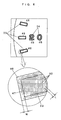
- Reference numeral 11 designates a housing, and this housing 11 includes a facing member 12 and a case body 13.
- the housing 11 contains three indicating instruments, that is, a speed indicator 14, a fuel indicator 15, and a water temperature indicator 16.
- the speed indicator 14 is larger than the fuel indicator 15 and the water temperature indicator 16, and is disposed between the fuel indicator 15 and the water temperature indicator 16.
- the speed indicator 14 includes a liquid crystal display element 17, a pointer 18, a lightguide member 19, and a stepping motor 20 (pointer driving means).
- the pointer 18 is rotated by the stepping motor 20, and indicates an index part 23 (fixed display part) of the liquid crystal display element 17.
- Reference numeral 21 designates a circuit board, and the stepping motor 20 is mounted on this circuit board 21.
- Reference numeral 22 designates a bulb (light emitting element), and this bulb 22 is connected to the circuit board 21.
- the liquid crystal display element 17 is illuminated through transmission of the light of the bulb 22.
- the light of the bulb 22 is guided by the lightguide member 19 to the pointer 18, and an indicating part 18a of the pointer 18 becomes luminous.
- the liquid crystal display element 17 is such that polarizing plates 30 and 31 are bonded to both surfaces of a liquid crystal cell 29 in which a liquid crystal 28 is sealed between a pair of translucent substrates 26 and 27 on which transparent electrode films 24 and 25 are formed (refer to Fig.4 ).
- the respective transparent electrode films 24 and 25 are formed into such a stripe shape that they are orthogonal to each other, and places where the transparent electrode films 24 are opposite to the transparent electrode films 25 become pixels 32.
- Reference numeral 33 designates a light shielding layer (light shielding part), and openings of this light shielding layer 33 are fixed display parts (index parts 23 and numerals 34).
- a hole part 36 through which a rotation shaft 35 of the stepping motor 20 passes is formed in the liquid crystal display element 17.
- the fuel indicator 15 and the water temperature indicator 16 respectively include character plates 37 and 38 and pointers 39 and 40.
- the character plates 37 and 38 are respectively such that black printing is applied to substrates made of translucent resin (for example, polycarbonate) except for index parts 41 and 42.
- the pointers 39 and 40 are rotated by stepping motors (not shown), and indicate the index parts 41 and 42 of the character plates 37 and 38.
- Reference numeral 43 designates a protection cover, and this protection cover 43 is fixed to the facing member 12 by a fixing pawl.
- circular openings 12a, 12b and 12c are respectively formed in the places corresponding to the liquid crystal display element 17, and the character plates 37 and 38.
- the liquid crystal display element 17 is of a negative display type in which the pixel 32 applied with a voltage is brought into a transmission state, and the pixel 32 applied no voltage is in a light shielding state.
- the liquid crystal display element 17 includes a variable display part 44 made of a region where the light shielding layer 33 is not provided, and this variable display part 44 displays alarm information such as a battery voltage shortage (see Fig. 2 ).
- this variable display part 44 displays alarm information such as a battery voltage shortage (see Fig. 2 ).
- Fig. 5 in order to bring the fixed display portions 23 and 34 into the transmission state, rectangular regions 45 and 46 wider than the fixed display portions 23 and 34 are brought into the transmission state.
- Fig. 6 is a view showing a second embodiment according to the invention.
- the second embodiment is different from the first embodiment only in a range in which a light shielding layer 46 is provided, and the other structure is the same as the first embodiment.
- the light shielding layer 46 is provided around each of the fixed display parts 23 and 34 to have a predetermined width W and a frame shape.
- the predetermined width W of the light shielding layer 46 is larger than a diagonal length L of a pixel 32.
- regions 47 respectively wider than the fixed display parts 23 and 34 and narrower than the light shielding layers 46 are brought into the transmission state.
- the fixed display parts 23 and 34 and the variable display part 44 can be provided on one display element (the liquid crystal display element 17), and the contours of the fixed display parts 23 and 34 are formed of the openings of the light shielding layer 33, so that the contours of the fixed display parts 23 and 34 do not become sawtooth.
- the light shielding layer 33 of the respective embodiments is laminated on the transparent electrode 24, for example, it may be formed on the front side surface of the translucent substrate 26 or may be formed on the front side surface of the polarizing plate 30.
- Figs. 7 to 10 are views showing a third embodiment not according to the invention.
- the third embodiment is different from the first embodiment only in a polarizing plate 50 and a liquid crystal display element 51, and the other structure is similar to the first embodiment, and accordingly, the same symbols are given to the same portions as those of the first embodiment, and the explanation is omitted.
- the display plate 50 is such that a light shielding part 53 is formed by printing on the front surface of a substrate 52 made of translucent resin (for example, polycarbonate).
- the light shielding part 53 is substantially arc-shaped when viewed from the front of the display plate 50. Openings are provided in the light shielding part 53, and the openings are index parts 54 and characters 55.
- the liquid crystal display element 51 is such that polarizing plates 30 and 31 are bonded to both surfaces of a liquid crystal cell 56 in which a liquid crystal 28 is sealed between a pair of translucent substrates 26 and 27 on which transparent electrode films 24 and 25 are formed.
- the respective transparent electrode films 24 and 25 are formed into such a stripe shape that they are orthogonal to each other, and places where the transparent electrode films 24 are opposite to the transparent electrode films 25 become pixels 58.
- Hole parts 59 and 60 through which a rotation shaft 35 of a stepping motor 20 passes are respectively formed in the display plate 50 and the liquid crystal display element 51.
- the liquid crystal display element 50 is of a negative display type in which a figure or a character to be displayed is brought into a transmission state, and for example, display alarm information such as a battery voltage shortage is displayed. Besides, as shown in Fig. 10 , in order to make light pass through the index part 54 and the character 55 of the display plate 50, rectangular regions 61 and 62 wider than the index part 54 and the character 55 are brought into the transmission state.
- Fig. 11 is a view showing a fourth embodiment according to the invention.
- the fourth embodiment is different from the third embodiment only in a range in which a light shielding part 64 is provided, and the other structure is similar to the third embodiment.
- the light shielding part 64 is provided around each of the index part 54 and the character 55 to have a predetermined width W and a frame shape.
- the predetermined width W of the light shielding part 64 is larger than a diagonal length L of the pixel 58.
- a region 65 wider than the index part 54 and the character 55 and narrower than an outer line of the light shielding part 64 is brought into the transmission state.
- Fig. 12 is a view showing a fifth embodiment not according to the invention.
- the fifth embodiment is different from the third embodiment only in a display plate 66, and the other structure is similar to the third embodiment.
- the display plate 66 is such that an index part 67 and a character 68 made of a colored layer are formed by printing on a substrate 69.
- the fixed display parts (the index parts 54 and 67, the characters 55 and 68) and the variable display part of the liquid crystal display element 51 can be provided in the speed indicator 14, and the contours of the fixed display parts do not become sawtooth.
- the liquid crystal display element 51 of the third to fifth embodiments is disposed behind the polarizing plate 50 or 66, the liquid crystal display element 51 may be disposed in front of the polarizing plate 50 or 66, and the same operation and effect can be obtained.
- the pointer driving means is the stepping motor 20, for example, it may be a crossed coil type movement.
- the light emitting element is the bulb 22, for example, it may be a light emitting diode.
- the display element is the liquid crystal display element 17 or 51, for example, it may be an organic EL display element.
- the present invention can be applied to a display device, and is particularly suitable for an on-vehicle display device.
Description
- The present invention relates to a dot matrix type display element and a display device using the dot matrix type display element.
- Hitherto, there is a dot matrix type liquid
crystal display element 1 as shown inFig. 13 . The liquidcrystal display element 1 includes a number ofpixels 2 provided in a matrix form. As shown inFig. 14 , the liquidcrystal display element 1 is such that polarizingplates liquid crystal cell 8 in which aliquid crystal 7 is sealed between a pair oftranslucent substrates transparent electrode films transparent electrode films transparent electrode films 3 are opposite to thetransparent electrode films 4 become thepixels 2. The liquidcrystal display element 1 can display various figures and characters (including numerals) by switching on/off therespective pixels 2. - However, since the contour of a displayed figure or character becomes sawtooth, there has been a problem that the figure or the character is disfigured. That is, since the shape of each of the
pixels 2 is square, in the case where the contour of the figure or the character, which is displayed by selectively switching on/off thepixels 2, is an oblique line or a curved line, the figure or the character becomes sawtooth. -
GB 2 056 067 A -
DE 197 57 564 discloses a display unit with a pointer driven by a measuring mechanism, for analogue display of a measured value in co-operation with fixed scale markings and variable scale information. The display may be a dot matrix display or a liquid crystal display cell. - The present invention has been made in view of the problem, and provides a display device which can display a character and a figure having an unsawtooth contour.
- The present invention provides a display device as recited in the claims.
-
-
Figs. 1 to 5 are views showing an embodiment not according to the invention, in whichFig. 1 is a front view of a liquid crystal display element,Fig. 2 is a front view of a display device,Fig. 3 is a sectional view of the display device,Fig. 4 is a sectional view showing the liquid crystal display element, andFig. 5 is a primary part enlarged view of the liquid crystal display element. -
Fig. 6 is a primary part enlarged view of a liquid crystal display element, showing an embodiment of the present invention. -
Figs. 7 to 10 are views showing an embodiment not according to the invention, in whichFig. 7 is a sectional view of a display device,Fig. 8 is a perspective view of a display plate and a liquid crystal display element,Fig. 9 is a sectional view of the display plate and the liquid crystal display element, andFig. 10 is a primary part enlarged view of the display plate. -
Fig. 11 is a primary part enlarged view of a display plate, showing an embodiment of the invention. -
Fig. 12 is a perspective view of a display plate and a liquid crystal display element, showing an embodiment not according to the invention. -
Figs. 13 and 14 are views showing the prior art, in whichFig. 13 is a front view of a liquid crystal display element, andFig. 14 is a sectional view of the liquid crystal display element. - Hereinafter, embodiments in which the present invention is applied to an on-vehicle display device, will be described with reference to the accompanying drawings.
Figs. 1 to 5 are views showing a first embodiment not according to the invention. -
Reference numeral 11 designates a housing, and thishousing 11 includes a facingmember 12 and acase body 13. Thehousing 11 contains three indicating instruments, that is, aspeed indicator 14, afuel indicator 15, and a water temperature indicator 16. Thespeed indicator 14 is larger than thefuel indicator 15 and the water temperature indicator 16, and is disposed between thefuel indicator 15 and the water temperature indicator 16. - The
speed indicator 14 includes a liquidcrystal display element 17, apointer 18, alightguide member 19, and a stepping motor 20 (pointer driving means). Thepointer 18 is rotated by the steppingmotor 20, and indicates an index part 23 (fixed display part) of the liquidcrystal display element 17. -
Reference numeral 21 designates a circuit board, and thestepping motor 20 is mounted on thiscircuit board 21.Reference numeral 22 designates a bulb (light emitting element), and thisbulb 22 is connected to thecircuit board 21. The liquidcrystal display element 17 is illuminated through transmission of the light of thebulb 22. The light of thebulb 22 is guided by thelightguide member 19 to thepointer 18, and an indicating part 18a of thepointer 18 becomes luminous. - The liquid
crystal display element 17 is such that polarizingplates liquid crystal cell 29 in which aliquid crystal 28 is sealed between a pair oftranslucent substrates transparent electrode films Fig.4 ). The respectivetransparent electrode films transparent electrode films 24 are opposite to thetransparent electrode films 25 becomepixels 32.Reference numeral 33 designates a light shielding layer (light shielding part), and openings of thislight shielding layer 33 are fixed display parts (index parts 23 and numerals 34). Ahole part 36 through which arotation shaft 35 of the steppingmotor 20 passes is formed in the liquidcrystal display element 17. - The
fuel indicator 15 and the water temperature indicator 16 respectively includecharacter plates pointers character plates index parts pointers index parts character plates -
Reference numeral 43 designates a protection cover, and thisprotection cover 43 is fixed to the facingmember 12 by a fixing pawl. In the facingmember 12,circular openings crystal display element 17, and thecharacter plates - The liquid
crystal display element 17 is of a negative display type in which thepixel 32 applied with a voltage is brought into a transmission state, and thepixel 32 applied no voltage is in a light shielding state. The liquidcrystal display element 17 includes avariable display part 44 made of a region where thelight shielding layer 33 is not provided, and thisvariable display part 44 displays alarm information such as a battery voltage shortage (seeFig. 2 ). Besides, as shown inFig. 5 , in order to bring thefixed display portions rectangular regions display portions -
Fig. 6 is a view showing a second embodiment according to the invention. The second embodiment is different from the first embodiment only in a range in which alight shielding layer 46 is provided, and the other structure is the same as the first embodiment. - The
light shielding layer 46 is provided around each of the fixeddisplay parts light shielding layer 46 is larger than a diagonal length L of apixel 32. In the liquidcrystal display element 17, in order to bring thefixed display parts regions 47 respectively wider than the fixeddisplay parts light shielding layers 46 are brought into the transmission state. - According to the first embodiment or the second embodiment, the
fixed display parts variable display part 44 can be provided on one display element (the liquid crystal display element 17), and the contours of thefixed display parts light shielding layer 33, so that the contours of thefixed display parts light shielding layer 33 of the respective embodiments is laminated on thetransparent electrode 24, for example, it may be formed on the front side surface of thetranslucent substrate 26 or may be formed on the front side surface of the polarizingplate 30. -
Figs. 7 to 10 are views showing a third embodiment not according to the invention. The third embodiment is different from the first embodiment only in a polarizingplate 50 and a liquidcrystal display element 51, and the other structure is similar to the first embodiment, and accordingly, the same symbols are given to the same portions as those of the first embodiment, and the explanation is omitted. - The
display plate 50 is such that alight shielding part 53 is formed by printing on the front surface of asubstrate 52 made of translucent resin (for example, polycarbonate). Thelight shielding part 53 is substantially arc-shaped when viewed from the front of thedisplay plate 50. Openings are provided in thelight shielding part 53, and the openings areindex parts 54 andcharacters 55. - The liquid
crystal display element 51 is such that polarizingplates liquid crystal cell 56 in which aliquid crystal 28 is sealed between a pair oftranslucent substrates transparent electrode films transparent electrode films transparent electrode films 24 are opposite to thetransparent electrode films 25 becomepixels 58. -
Hole parts rotation shaft 35 of astepping motor 20 passes are respectively formed in thedisplay plate 50 and the liquidcrystal display element 51. - The liquid
crystal display element 50 is of a negative display type in which a figure or a character to be displayed is brought into a transmission state, and for example, display alarm information such as a battery voltage shortage is displayed. Besides, as shown inFig. 10 , in order to make light pass through theindex part 54 and thecharacter 55 of thedisplay plate 50,rectangular regions index part 54 and thecharacter 55 are brought into the transmission state. -
Fig. 11 is a view showing a fourth embodiment according to the invention. The fourth embodiment is different from the third embodiment only in a range in which alight shielding part 64 is provided, and the other structure is similar to the third embodiment. - The
light shielding part 64 is provided around each of theindex part 54 and thecharacter 55 to have a predetermined width W and a frame shape. The predetermined width W of thelight shielding part 64 is larger than a diagonal length L of thepixel 58. In the liquidcrystal display element 51, in order to make light pass through theindex part 54 and thecharacter 55 of thedisplay part 50, aregion 65 wider than theindex part 54 and thecharacter 55 and narrower than an outer line of thelight shielding part 64 is brought into the transmission state. -
Fig. 12 is a view showing a fifth embodiment not according to the invention. The fifth embodiment is different from the third embodiment only in adisplay plate 66, and the other structure is similar to the third embodiment. - The
display plate 66 is such that anindex part 67 and acharacter 68 made of a colored layer are formed by printing on asubstrate 69. Ahole part 70 through which arotation shaft 35 of a steppingmotor 20 passes is formed in thedisplay plate 66. - According to the third to fifth embodiments, the fixed display parts (the
index parts characters 55 and 68) and the variable display part of the liquidcrystal display element 51 can be provided in thespeed indicator 14, and the contours of the fixed display parts do not become sawtooth. Incidentally, although the liquidcrystal display element 51 of the third to fifth embodiments is disposed behind thepolarizing plate crystal display element 51 may be disposed in front of thepolarizing plate - Besides, in the first to fifth embodiments, although the pointer driving means is the stepping
motor 20, for example, it may be a crossed coil type movement. Besides, although the light emitting element is thebulb 22, for example, it may be a light emitting diode. Besides, although the display element is the liquidcrystal display element - The present invention can be applied to a display device, and is particularly suitable for an on-vehicle display device.
Claims (3)
- A display device comprising:a pointer (18) including an indicating part (18a);pointer driving means (20) for rotating the pointer (18); anda display element (17) including a plurality of index parts (23) disposed for indication by the indicating part (18a),characterized in thatthe display element (17) comprises a pair of translucent substrates (26, 27), stripe-shaped transparent electrode films (24, 25) respectively formed on the translucent substrates (26, 27) to define a plurality of pixels (32), and a light shielding part (46) provided on at least one of the translucent substrates (26, 27), andwherein each of said index parts (23) comprises a light shielding part (46) formed to frame a group of pixels (32), said light shielding part (46) having a width, W, larger than a diagonal length, L, of a pixel (32), andwherein said light shielding part (46) shields transmission from pixels (32) and from portions of pixels (32) disposed beneath said light shielding part (46) so as to provide an index part (23) having a substantially smooth contour when said group of pixels (32) is selectively brought into a transmission state.
- A display device according to claim 1, characterized in that the display element (17) includes a hole part (36) formed in a place corresponding to a rotation shaft (35) of the pointer driving means (20).
- A display device according to claim 1, characterized in that a light emitting element (22) for illuminating the display element (17) from behind is provided.
Applications Claiming Priority (5)
| Application Number | Priority Date | Filing Date | Title |
|---|---|---|---|
| JP2000221568 | 2000-07-24 | ||
| JP2000221568 | 2000-07-24 | ||
| JP2001052563 | 2001-02-27 | ||
| JP2001052563 | 2001-02-27 | ||
| PCT/JP2001/005736 WO2002009073A1 (en) | 2000-07-24 | 2001-07-02 | Display element and display device using display element |
Publications (3)
| Publication Number | Publication Date |
|---|---|
| EP1235197A1 EP1235197A1 (en) | 2002-08-28 |
| EP1235197A4 EP1235197A4 (en) | 2005-03-23 |
| EP1235197B1 true EP1235197B1 (en) | 2010-08-25 |
Family
ID=26596491
Family Applications (1)
| Application Number | Title | Priority Date | Filing Date |
|---|---|---|---|
| EP01945776A Expired - Lifetime EP1235197B1 (en) | 2000-07-24 | 2001-07-02 | Display element and display device using display element |
Country Status (4)
| Country | Link |
|---|---|
| US (1) | US20020135713A1 (en) |
| EP (1) | EP1235197B1 (en) |
| DE (1) | DE60142886D1 (en) |
| WO (1) | WO2002009073A1 (en) |
Families Citing this family (8)
| Publication number | Priority date | Publication date | Assignee | Title |
|---|---|---|---|---|
| JP4392171B2 (en) * | 2003-01-20 | 2009-12-24 | カルソニックカンセイ株式会社 | Vehicle display device |
| DE10303278A1 (en) * | 2003-01-28 | 2004-08-12 | Siemens Ag | pointer instrument |
| JP4100360B2 (en) * | 2004-03-05 | 2008-06-11 | 株式会社デンソー | Simple matrix type liquid crystal display device |
| JP2006343728A (en) * | 2005-05-13 | 2006-12-21 | Toshiba Matsushita Display Technology Co Ltd | Liquid crystal display device |
| DE102005036004A1 (en) * | 2005-08-01 | 2007-02-08 | GM Global Technology Operations, Inc., Detroit | Display instrument with a dial and a rotating pointer |
| WO2007132574A1 (en) * | 2006-05-12 | 2007-11-22 | Sharp Kabushiki Kaisha | Display panel and display |
| DE102007036887A1 (en) * | 2007-08-04 | 2009-02-19 | Paragon Ag | Indicating instrument for motor vehicle, has thin-film transistor-display on which analog values are displayed by digital display elements, and analog round pointer instrument integrated with thin-film transistor-display |
| US9228864B2 (en) * | 2012-12-18 | 2016-01-05 | Continental Automotive Systems, Inc. | Displaying graphics on a instrument mask |
Family Cites Families (7)
| Publication number | Priority date | Publication date | Assignee | Title |
|---|---|---|---|---|
| DE2931327A1 (en) * | 1979-08-02 | 1981-02-19 | Rau Swf Autozubehoer | DISPLAY SYSTEM, ESPECIALLY FOR MOTOR VEHICLES |
| JPS58176677A (en) * | 1982-04-09 | 1983-10-17 | 株式会社日立製作所 | Liquid crystal display |
| JPH02166420A (en) * | 1988-12-20 | 1990-06-27 | Seiko Epson Corp | Liquid crystal electrooptic element |
| JPH0344624U (en) * | 1989-09-08 | 1991-04-25 | ||
| DE19757564A1 (en) * | 1997-12-23 | 1999-07-01 | Mannesmann Vdo Ag | Display device |
| DE19845579A1 (en) * | 1998-10-02 | 2000-04-13 | Mannesmann Vdo Ag | Display device |
| JP2000111674A (en) * | 1998-10-07 | 2000-04-21 | Citizen Watch Co Ltd | Timepiece |
-
2001
- 2001-07-02 US US10/070,830 patent/US20020135713A1/en not_active Abandoned
- 2001-07-02 WO PCT/JP2001/005736 patent/WO2002009073A1/en active Application Filing
- 2001-07-02 DE DE60142886T patent/DE60142886D1/en not_active Expired - Lifetime
- 2001-07-02 EP EP01945776A patent/EP1235197B1/en not_active Expired - Lifetime
Also Published As
| Publication number | Publication date |
|---|---|
| US20020135713A1 (en) | 2002-09-26 |
| EP1235197A4 (en) | 2005-03-23 |
| DE60142886D1 (en) | 2010-10-07 |
| EP1235197A1 (en) | 2002-08-28 |
| WO2002009073A1 (en) | 2002-01-31 |
Similar Documents
| Publication | Publication Date | Title |
|---|---|---|
| US10192522B2 (en) | Multi-layered display device | |
| US10406918B2 (en) | Display device | |
| US6379015B2 (en) | Indicating instrument with an illuminated pointer disposed behind the dial | |
| KR100942850B1 (en) | Display device | |
| US6281788B1 (en) | Indicating instrument | |
| EP1235197B1 (en) | Display element and display device using display element | |
| EP1067502B1 (en) | Display | |
| JP5297952B2 (en) | Display device and vehicular instrument device including the display device | |
| JP6585430B2 (en) | Display device | |
| JP2003161650A (en) | Indicator instrument device | |
| JPH09207625A (en) | Display unit | |
| JP4756294B2 (en) | Indicator device | |
| US20170176659A1 (en) | Combination display instrument | |
| JP2002351358A (en) | Display device | |
| JPH11170890A (en) | Display device for vehicle | |
| WO2018139432A1 (en) | Display device | |
| JPH09265087A (en) | Liquid crystal display device | |
| JPH09318395A (en) | Instrument for vehicle | |
| JP2002316557A (en) | Display device for vehicle | |
| JP6127819B2 (en) | Vehicle display device | |
| JP2018097233A (en) | Liquid crystal display device | |
| JP2001067006A (en) | Display device | |
| CN109203993B (en) | Vehicle display device | |
| JPH0624811Y2 (en) | Liquid crystal display | |
| JP6248693B2 (en) | Display device |
Legal Events
| Date | Code | Title | Description |
|---|---|---|---|
| PUAI | Public reference made under article 153(3) epc to a published international application that has entered the european phase |
Free format text: ORIGINAL CODE: 0009012 |
|
| 17P | Request for examination filed |
Effective date: 20020326 |
|
| AK | Designated contracting states |
Kind code of ref document: A1 Designated state(s): AT BE CH CY DE DK ES FI FR GB GR IE IT LI LU MC NL PT SE TR |
|
| RBV | Designated contracting states (corrected) |
Designated state(s): AT BE CH CY DE FR GB IT LI SE |
|
| A4 | Supplementary search report drawn up and despatched |
Effective date: 20050204 |
|
| RIC1 | Information provided on ipc code assigned before grant |
Ipc: 7G 01D 7/00 B Ipc: 7B 60K 35/00 B Ipc: 7G 09F 9/00 A Ipc: 7G 01D 11/28 B Ipc: 7G 01D 13/00 B Ipc: 7B 60Q 3/04 B Ipc: 7G 09F 9/30 B |
|
| RBV | Designated contracting states (corrected) |
Designated state(s): DE FR GB IT SE |
|
| 17Q | First examination report despatched |
Effective date: 20070608 |
|
| GRAP | Despatch of communication of intention to grant a patent |
Free format text: ORIGINAL CODE: EPIDOSNIGR1 |
|
| GRAS | Grant fee paid |
Free format text: ORIGINAL CODE: EPIDOSNIGR3 |
|
| GRAA | (expected) grant |
Free format text: ORIGINAL CODE: 0009210 |
|
| AK | Designated contracting states |
Kind code of ref document: B1 Designated state(s): DE FR GB IT SE |
|
| REG | Reference to a national code |
Ref country code: GB Ref legal event code: FG4D |
|
| REF | Corresponds to: |
Ref document number: 60142886 Country of ref document: DE Date of ref document: 20101007 Kind code of ref document: P |
|
| PG25 | Lapsed in a contracting state [announced via postgrant information from national office to epo] |
Ref country code: SE Free format text: LAPSE BECAUSE OF FAILURE TO SUBMIT A TRANSLATION OF THE DESCRIPTION OR TO PAY THE FEE WITHIN THE PRESCRIBED TIME-LIMIT Effective date: 20100825 |
|
| PG25 | Lapsed in a contracting state [announced via postgrant information from national office to epo] |
Ref country code: IT Free format text: LAPSE BECAUSE OF FAILURE TO SUBMIT A TRANSLATION OF THE DESCRIPTION OR TO PAY THE FEE WITHIN THE PRESCRIBED TIME-LIMIT Effective date: 20100825 |
|
| PLBE | No opposition filed within time limit |
Free format text: ORIGINAL CODE: 0009261 |
|
| STAA | Information on the status of an ep patent application or granted ep patent |
Free format text: STATUS: NO OPPOSITION FILED WITHIN TIME LIMIT |
|
| 26N | No opposition filed |
Effective date: 20110526 |
|
| REG | Reference to a national code |
Ref country code: DE Ref legal event code: R097 Ref document number: 60142886 Country of ref document: DE Effective date: 20110526 |
|
| GBPC | Gb: european patent ceased through non-payment of renewal fee |
Effective date: 20110702 |
|
| REG | Reference to a national code |
Ref country code: FR Ref legal event code: ST Effective date: 20120330 |
|
| PG25 | Lapsed in a contracting state [announced via postgrant information from national office to epo] |
Ref country code: FR Free format text: LAPSE BECAUSE OF NON-PAYMENT OF DUE FEES Effective date: 20110801 Ref country code: DE Free format text: LAPSE BECAUSE OF NON-PAYMENT OF DUE FEES Effective date: 20120201 |
|
| REG | Reference to a national code |
Ref country code: DE Ref legal event code: R119 Ref document number: 60142886 Country of ref document: DE Effective date: 20120201 |
|
| PG25 | Lapsed in a contracting state [announced via postgrant information from national office to epo] |
Ref country code: GB Free format text: LAPSE BECAUSE OF NON-PAYMENT OF DUE FEES Effective date: 20110702 |