EP1235140A1 - Verfahren zur Verzweigungsverwaltung in einem Prozessor - Google Patents
Verfahren zur Verzweigungsverwaltung in einem Prozessor Download PDFInfo
- Publication number
- EP1235140A1 EP1235140A1 EP02290402A EP02290402A EP1235140A1 EP 1235140 A1 EP1235140 A1 EP 1235140A1 EP 02290402 A EP02290402 A EP 02290402A EP 02290402 A EP02290402 A EP 02290402A EP 1235140 A1 EP1235140 A1 EP 1235140A1
- Authority
- EP
- European Patent Office
- Prior art keywords
- instruction
- register
- value
- counter
- fact
- Prior art date
- Legal status (The legal status is an assumption and is not a legal conclusion. Google has not performed a legal analysis and makes no representation as to the accuracy of the status listed.)
- Withdrawn
Links
- 238000000034 method Methods 0.000 title claims abstract description 22
- 238000012545 processing Methods 0.000 claims abstract description 83
- 239000003607 modifier Substances 0.000 claims description 27
- 101000578349 Homo sapiens Nucleolar MIF4G domain-containing protein 1 Proteins 0.000 claims description 7
- 102100027969 Nucleolar MIF4G domain-containing protein 1 Human genes 0.000 claims description 7
- 230000008569 process Effects 0.000 claims description 5
- 238000011161 development Methods 0.000 claims description 4
- CQIZBIFTOGBKDB-UHFFFAOYSA-N 4-cyclohexyl-1-methyl-3,6-dihydro-2h-pyridine Chemical compound C1N(C)CCC(C2CCCCC2)=C1 CQIZBIFTOGBKDB-UHFFFAOYSA-N 0.000 claims description 3
- 101100076239 Drosophila melanogaster Mctp gene Proteins 0.000 claims description 3
- 101100123587 Saccharomyces cerevisiae (strain ATCC 204508 / S288c) HDA3 gene Proteins 0.000 claims description 2
- 101100297842 Schizosaccharomyces pombe (strain 972 / ATCC 24843) plo1 gene Proteins 0.000 claims description 2
- 230000008859 change Effects 0.000 claims description 2
- 101000937642 Homo sapiens Malonyl-CoA-acyl carrier protein transacylase, mitochondrial Proteins 0.000 claims 1
- 101000590830 Homo sapiens Monocarboxylate transporter 1 Proteins 0.000 claims 1
- 102100027329 Malonyl-CoA-acyl carrier protein transacylase, mitochondrial Human genes 0.000 claims 1
- 101100169932 Saccharomyces cerevisiae (strain ATCC 204508 / S288c) DCD1 gene Proteins 0.000 description 8
- 101100235787 Schizosaccharomyces pombe (strain 972 / ATCC 24843) pim1 gene Proteins 0.000 description 8
- 238000007726 management method Methods 0.000 description 6
- 240000008042 Zea mays Species 0.000 description 4
- 230000004048 modification Effects 0.000 description 4
- 238000012986 modification Methods 0.000 description 4
- 238000002360 preparation method Methods 0.000 description 4
- 230000006870 function Effects 0.000 description 3
- 238000012360 testing method Methods 0.000 description 3
- 230000005540 biological transmission Effects 0.000 description 2
- 238000004364 calculation method Methods 0.000 description 2
- 230000000694 effects Effects 0.000 description 2
- 238000012546 transfer Methods 0.000 description 2
- 241001080024 Telles Species 0.000 description 1
- 238000012550 audit Methods 0.000 description 1
- 230000015572 biosynthetic process Effects 0.000 description 1
- 230000001143 conditioned effect Effects 0.000 description 1
- 239000004020 conductor Substances 0.000 description 1
- 235000021183 entrée Nutrition 0.000 description 1
- 230000006872 improvement Effects 0.000 description 1
- 238000004519 manufacturing process Methods 0.000 description 1
- 230000007246 mechanism Effects 0.000 description 1
- 238000012163 sequencing technique Methods 0.000 description 1
- 238000003786 synthesis reaction Methods 0.000 description 1
- 238000012795 verification Methods 0.000 description 1
Images


Classifications
-
- G—PHYSICS
- G06—COMPUTING; CALCULATING OR COUNTING
- G06F—ELECTRIC DIGITAL DATA PROCESSING
- G06F9/00—Arrangements for program control, e.g. control units
- G06F9/06—Arrangements for program control, e.g. control units using stored programs, i.e. using an internal store of processing equipment to receive or retain programs
- G06F9/30—Arrangements for executing machine instructions, e.g. instruction decode
- G06F9/38—Concurrent instruction execution, e.g. pipeline or look ahead
- G06F9/3802—Instruction prefetching
- G06F9/3804—Instruction prefetching for branches, e.g. hedging, branch folding
-
- G—PHYSICS
- G06—COMPUTING; CALCULATING OR COUNTING
- G06F—ELECTRIC DIGITAL DATA PROCESSING
- G06F9/00—Arrangements for program control, e.g. control units
- G06F9/06—Arrangements for program control, e.g. control units using stored programs, i.e. using an internal store of processing equipment to receive or retain programs
- G06F9/30—Arrangements for executing machine instructions, e.g. instruction decode
- G06F9/30094—Condition code generation, e.g. Carry, Zero flag
-
- G—PHYSICS
- G06—COMPUTING; CALCULATING OR COUNTING
- G06F—ELECTRIC DIGITAL DATA PROCESSING
- G06F9/00—Arrangements for program control, e.g. control units
- G06F9/06—Arrangements for program control, e.g. control units using stored programs, i.e. using an internal store of processing equipment to receive or retain programs
- G06F9/30—Arrangements for executing machine instructions, e.g. instruction decode
- G06F9/38—Concurrent instruction execution, e.g. pipeline or look ahead
- G06F9/3836—Instruction issuing, e.g. dynamic instruction scheduling or out of order instruction execution
- G06F9/3842—Speculative instruction execution
Definitions
- the invention relates to processors, in particular the digital signal processing processors (DSP: “Digital Signal Processors "in English), and more specifically management instructions for connection within such a processor.
- DSP digital signal processing processors
- a processor generally comprises several units of processing operating in parallel. Conventionally, it is provided as processing units, an arithmetic and logic module, a module and a connection management module. Besides these units of processing, the processor generally comprises a central unit (unit ) which dialogs with the program memory and delivers to different processing units, basic instructions again commonly called micro-instructors.
- connection which are issued to module or branch management unit.
- An instruction from branching is an instruction involving a break in sequence in normal sequencing of instructions.
- a program counter is arranged for issue successive values corresponding to addresses instructions in program memory, an instruction to branching will modify the value at a given time current program counter to force the pointer address on a given address of the program memory.
- connection instructions can be conditional, for example kept, as will be explained below.
- connection instructions require to reach the connection unit before being effectively processed.
- the unity of connection is generally "at the bottom" of the pipelined architecture of the processor, which implies a relatively long latency before a branch instruction is actually processed.
- the invention aims to provide a solution to this problem.
- the object of the invention is to propose a mechanism for managing connection instructions completely different from the one up to now, and which allows an overall improvement in the latency of connection.
- the invention applies very particularly but not necessarily to a processor with a so-called “decoupled” architecture.
- the invention therefore proposes a method for managing instructions connection within a processor, the processor comprising a program memory containing program instructions, and a processor core containing several processing units and one unit Central.
- the central unit upon receipt of a program instruction, issues corresponding instructions to the different units of treatment.
- the core of processor being clocked by a clock signal, an instruction of connection received by the central unit during a current cycle of the clock signal, is processed during this current cycle.
- connection module is transferred in the central unit, which allows processing much faster connection instructions.
- connection instructions can use the content of one or more address pointing registers which are not not necessarily incorporated in the central unit. So, as an example, these address pointing registers can be incorporated into a first processing unit, for example the addressing unit. And, the fact of move the connection function in the central unit, place the problem of the validity of the content of address pointing registers when these are incorporated into a processing unit different from the central unit, and that they are accessed in later time cycles in the current cycle during which the branch instruction is examined.
- the invention also provides a solution to this problem.
- a first processing unit for example the addressing unit, contains at least one address pointing register
- a branch instruction uses the content of at least one of the registers address pointing
- a check is made at the start of said current cycle the validity of the content of the clocking register concerned.
- said connection instruction is then effectively received by the unit central and processed if the content is declared valid. And, if not, this connection instruction is kept pending processing (for example in a buffer register at the head of the central unit) until the content is declared valid.
- This validity check may be within the meaning of the direct invention or indirect. More specifically, it could be done directly on the architectural pointing register contained in the addressing unit. But it can also be done indirectly on this architectural register. So, a particularly simple way to check the validity of the content of address pointing registers, compatible with latency minimum, consists of copying the content of each score register address in a duplicate address pointing register. Control of the validity of the content of the clocking register concerned, is then a checking the validity of the content of the corresponding duplicate register.
- This validity check takes into account the management of amending instructions intended to modify the content of a register of address pointing.
- each time once the central unit receives a modification instruction intended to modify the content of an address pointing register, and temporally older than a branch instruction involving this register of address pointing, checking the validity of the content of the duplicated register correspondent takes into account the fact that this modifier instruction was or was not processed by said first unit, for example the unit addressing.
- a guarded instruction is an instruction affected by a so-called "guard" indication, in practice a guard bit can take the value 0 or 1. The kept instruction will then be executed or not depending the value of the guard bit, i.e. the guard indication. All the binary values of the guard indications, which may be one of sixteen for example, are contained in a register called “register of custody indications ". This centralized register is incorporated into a processing unit, for example the arithmetic and logic unit, and contains the current values of the indications or bits of keep. The values of these guard indications can be modified by specific instructions called "modifying instructions".
- the processing unit which receives this guarded instruction and who does not have direct access to the register of care indications requires a transfer of the value of the guard indication from the unit of processing which holds the register of custody indications.
- the issuance of a guarded instruction to a processing unit which does not hold the register of indications of care causes the issue to the treatment unit which is the keeper of the register of indications for custody, of a so-called "transmission" instruction which is intended to transmit to the processing unit which receives the kept instruction, the value the care indication associated with this guarded instruction.
- stage FIFO first in-first instruction memory released
- the instruction kept is maintained in the head stage (stage FIFO (first in-first) instruction memory released), associated with this processing unit, until this last receives from the processing unit which holds the register of guard indications, said value of the guard indication associated with this instruction kept. It is only when the processing unit that holds the register of indications of care, will have executed the instruction of transmission, that the corresponding value of the guard indication will be transmitted to the requesting processing unit, so that it can or not carry out his guarded instruction.
- the invention also provides a solution to this problem.
- a second processing unit for example the arithmetic and logical unit, contains a guard indication register, in the presence of a kept connection instruction
- said guarded branch instruction is actually received by the unit central and processed (i.e. it will be executed or not depending on the value of the care indication) if the value of the care indication corresponding is declared valid. And, if not, this kept branch instruction is kept pending processing until the value of the corresponding guard indication is declared valid.
- this control can be direct or indirect. So, analogously to what has was mentioned for the copying of address pointing registers, it is advantageously provided, according to an embodiment of the method, that the content of the care indication register is copied into a register duplicate custody instructions. Checking the validity of the value of a guard indication is then a check on the validity of the value of the corresponding custody indication contained in the duplicated register of guard indications.
- a modifying instruction intended to modify the value of a indication of custody contained in the register of custody indications, and temporally older than a guarded branch instruction each time that the central unit receives a modification instruction intended to modify the value of a guard indication and temporally older than a connection instruction kept by said guard indication, the validity check of the value of the indication of care contained in the duplicate register takes into account that this instruction modifier was or was not processed by said second unit, that is to say the unit which effectively holds the register of indications of care, to know the arithmetic and logical unity.
- the read counter and the write counter have advantageously an identical binary size equal to the depth of the second thesis.
- an overflow bit changing from value to each time the corresponding counter returns to its initial value.
- the memory is also memorized current value of the write counter overflow bit.
- the determination of the always present character of the instruction modifier in the second memory also takes into account the result of the comparison of the current value of the overflow bit of the read counter with said stored value of the overflow bit of the write counter.
- the invention also relates to a processor, in particular a digital signal processing processor, comprising a program memory containing the program instructions, and a processor core containing several processing units and one unit central unit capable, on receipt of a program instruction, of delivering the corresponding instructions for the different processing units.
- a processor in particular a digital signal processing processor, comprising a program memory containing the program instructions, and a processor core containing several processing units and one unit central unit capable, on receipt of a program instruction, of delivering the corresponding instructions for the different processing units.
- the central unit includes a connection module capable of receiving an instruction from connection during a current clock cycle, and to process this connection instruction during this current cycle.
- a first unit processing unit for example the addressing unit, contains at least one address pointing register.
- a branch instruction uses the content of at least one of the address pointing registers.
- the unit central comprises first validity control means capable of at the start of said current cycle, check the validity of the content of the said score register concerned. And, the instruction of connection is actually received by the central unit and processed if the content is declared valid, while otherwise this branch instruction is kept pending processing until that the content is declared valid.
- the central unit includes, for each address pointing register, a register address pointing duplicate, the content of which is a copy of the register of corresponding address pointing.
- the first means of controlling validity are then able to check the validity of the contents of the register corresponding duplicate.
- a second processing unit for example the arithmetic unit and logic, contains a register of guard indications.
- Central unity has second means of valid validity control in the presence a guarded connection instruction, to be carried out at the start of said cycle current, checking the validity of the value of the guard indication assigned to said branch instruction contained in the register custody indication.
- Said kept connection instruction is actually received by the central processing unit and processed, if the value of the corresponding custody indication is declared valid, and, in the case otherwise, this kept branch instruction is kept in waiting for processing until the value of the guard indication be declared valid.
- the central unit contains a duplicate register of indications of care, the content of which is a copy of the register of indications of care incorporated in the second processing unit.
- the second means of checking validity are able to check the validity of the value of a care indication contained in the duplicate register of indications of care.
- the central unit includes second means of preparation, suitable, whenever the central unit receives a modification instruction intended to modify the value of a guard indication and temporally older than a connection indication kept by said guard indication, at develop a second flag signal representative of the fact that this modifying instruction has been processed or not by said second unit.
- the logic means deliver the second flag signal and the second validity check means check the value of this second flag signal.
- the second unit includes control means capable of determining the presence or the absence of the modifier instruction in the memory.
- the counter write and the read counter have an identical binary size equal to the depth of the second memory.
- Each counter has an associated overflow bit changing value each time the counter corresponding returns to its initial value.
- Each elementary register further includes a one-bit auxiliary field.
- the first block of command is then suitable, each time an instruction modifying the value of a guard indication is stored in the second memory, at also store the current value of the counter overflow bit writing in the auxiliary field of the corresponding elementary register.
- the second control block then comprises means for auxiliary comparisons able to compare the current value of the bit of overflow of the reading counter with the content of the auxiliary field.
- auxiliary comparison means include for example a NON OR EXCLUSIVE logic gate (XNOR in English).
- the reference PROC designates a processor, by example a digital signal processing processor.
- the PROC processor has a PM program memory containing the program instructions. This program memory is addressed by a PMC memory controller which cooperates with the CR core of the processor. The address in program memory is defined from of the current value of a PC program counter.
- the processor core CR also dialogues with a DMC memory controller that controls access to a memory DMM data, for example two SRAM memory banks.
- the core of the processor comprises a central processing unit CU and several processing units, here two processing units separate DU and AU treatment.
- the central unit CU is the master unit of the system. In general, she manages all ordering activities. More specifically, it issues program addresses to the PMC memory controller and distributes the corresponding instructions to the different processing units. More specifically, the central processing unit CU has a PFAL interface with the PMC memory controller, which in particular performs formatting of instructions into instructions ready to be decoded.
- the instructions are then decoded in a decoder which in fact here comprises two successive decoding blocks.
- Function of the decoder is to transform each machine instruction into a or several micro-instructions which can be processed by different processing units.
- instructions a micro-instruction.
- a special feature of the CPU central processing unit according to the invention resides in the fact that it comprises the connection module BRU which processes the connection instructions.
- the first decoding block DCD1 goes, in presence of a connection instruction at the output of the PFAL interface, issue after a validity check, this connection instruction to BRU connection module. This is done during a signal cycle clock that clock the processor core. And, according to the invention, to from the moment when the DCD 1 decoding block has performed a positive validity on the detail of which we will return below, the module of BRU connection processes this connection instruction in the same current cycle and develops the new value of the PC program counter which will allow to point in the program memory to the new selected address.
- the DCD1 decoding block does not deliver not the connection instruction to the BRU connection module and this connection instruction remains pending in the PFAL interface.
- the instructions different from a branch instruction are partly decoded in the DCD1 block and partly (typically at during the next clock cycle) in the other decoding block at the output from which are available the micro-instructions which can be processed by the AU or DU processing units.
- DISP Disposed referral means in language English) sends the instructions generated by the decoding block to processing units for which these instructions are intended.
- the DU processing unit is an arithmetic and logic unit which performs most of the arithmetic operations.
- the AU unit is an addressing unit that performs calculations effective address required to address the operands in the memory.
- This AU unit contains all the registers necessary for this task as well as address pointing registers Px.
- x denotes the number of the address pointing register P.
- an instruction of connection uses one of the address pointing registers, for example example the register P3 and uses the content of this register for the calculation of the new value of the PC program counter.
- the AU unit includes a FIFO type memory, referenced AIDQ, intended to store the instructions intended for this AU unit, in in particular the modifying instructions intended to modify the values address pointing registers Px, in particular the register P3.
- AIDQ a FIFO type memory
- the processing unit DU includes a second memory of the FIFO type, referenced DIDQ, intended to store the instructions intended to these DU units, in particular as will be seen in more detail below modifier instructions for modifying values of guard indications.
- DMI which contains in particular another memory of the FIFO type, referenced LDQ, which is intended to receive and temporarily store data contained in the SRAM memory banks.
- one of the processing units for example the DU unit, includes a register of GR care indications.
- This register stores the current values of all the guard indications, which are for example sixteen in number.
- This register of care indications is located at the bottom of the pipelined structure of the DU unit.
- the reference EX designates the pipelined structure of the DU unit floors. In the rest of the text, and to for the sake of simplification, it will be assumed that the DU unit has only one single stage of pipeline between the output of the DIDQ memory and the register of guard indications GR.
- the processor described here has a decoupled architecture, allowing, after an initial latency, a speed of execution of the instructions more important.
- certain instructions call to data stored in the DMM data memory are partitioned into a micro-instruction intended for the DU unit and into a micro-instruction intended for the AU unit to develop said data memory.
- a load instruction in a register of stored data is partitioned into two micro-instructions or instructions.
- a first instruction is sent to the addressing unit (AU) which calculates the effective address of the data in data memory.
- the other instruction which is an instruction from loading in the concerned register, is temporarily stored in the DIDQ memory associated with the arithmetic and logical unit. This second instruction remains pending until the memorized, elaborated data by the addressing unit, is available. When this is the case, updating day of the concerned register is actually carried out.
- the addressing unit After an initial latency period, the addressing unit has taken ahead of the arithmetic and logical unit. The machine is then "Decoupled". In return, seen from the arithmetic and logical unity, the "fictitious" latency is zero.
- a branch instruction uses the content of at least one of the address pointing registers Px, for example the register P3 contained in the unit AU.
- the CU unit includes first means validity check MCV1, able to perform at the start of the current cycle the clock signal during which the DCD1 decoding block is ready to receive a connection instruction, check the validity of the content of the relevant time register Px.
- this control of validity is carried out on a duplicate PxC address pointing register.
- This duplicated PxC register is physically connected by a conductor electric, to the address pointing register Px contained in the AU unit.
- effective duplication of the contents of the Px register in the duplicated PxC register is conditioned by a control signal SC 10 delivered by a logic gate PL4 making part of the first MCTP development means.
- first means are generally suitable, whenever the central unit receives a modifying instruction intended to modify the contents of an address pointing register, for example the Px register, this amending instruction being temporarily older than a connection instruction involving this Px register, to prepare a first flag signal SGD1 representative of the fact that this instruction modifier was or was not processed by the AU unit.
- the plug-in module will use the content duplicate registers, but the architectural score registers addresses that are subject to change, are located in the unit AU, and therefore at much lower levels of the pipeline, we have to make sure, before using the contents of a duplicate register, which there is not in the pipeline, a temporally older modifier statement, which has not yet updated the architectural address register corresponding.
- the means of incrementation are suitable, whenever a amending instruction intended to modify the content of a address pointing is received by the DCD1 decoder of the central unit, at increment the counter CPTPx.
- the means of decrementation are suitable, whenever this modifying instruction has been processed by the AU unit, to be decremented the counter.
- the means of decrementation are controlled by a logic signal SC0 from the AU unit which indicates that the instruction modifier was actually processed by the AU unit.
- the logic signal SC1 takes take into account the value of the instruction indication of custody guarded modifier.
- the processor initializes, the CPTPx counter is initialized to zero.
- the first MCV1 validity checking means which are in fact means testing simply the value 0 or 1 of the signal SGD1, carry out a control of the validity of the content of the duplicated PxC register.
- This duplicate register is considered to have valid content if signal SGD1 has a value logic corresponding to a zero value of the CPTPx counter.
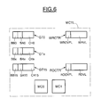
- FIG. 4 very briefly illustrates an implementation of execution of a branch instruction.
- a SALW register contains the current value of the PC program counter. This value is added to the value of the duplicated PxC register to provide the new PC counter value.
- the central unit has second means for controlling validity MCV2 (figure 2) able, in the presence of an instruction guarded connection, to be carried out at the start of the current cycle the validity of the value of the guard indication assigned to said instruction of guarded connection, this indication of guard being contained in the register of guard indications GR.
- validity MCV2 figure 2
- the kept connection instruction will then be effectively received by the central unit and processed by the BRU connection module in the same current clock cycle, if the value of the guard indication corresponding is declared valid. Otherwise, this kept branch instruction is kept pending processing until the value of the corresponding guard indication is declared valid.
- the central unit includes a duplicate register of RCMP custody notices ( Figure 5) the content of which is a copy of the register of guard indications GR.
- the RGC duplicate register is materially linked to the GR register.
- the central unit furthermore comprises second means of suitable MCTG development, each time the central unit receives a GMIx modifier instruction, intended to modify the value of a Gx guard indication, and temporally older than a connection instruction kept by said guard indication Gx, at develop a second flag signal DEGxV representative of the fact that this modifying instruction has or has not been processed by the DU unit.
- a GMIx modifier instruction can be between the decoder and the entry of the DIDQ memory, to use a CPTx counter (actually a down counter) clocked by the clock signal and initialized by the decoder block DCD1 using a RSx signal when this decodes the GMIx instruction.
- the counter is thus initialized to an initial value corresponding to the number of cycles required for the GMIx modifier instruction to be stored in DIDQ memory.
- the number of cycles clock can be two or three.
- the MCTL control means include a reading counter RDCTR, circular, incremented each time an instruction, what whatever it is, is extracted from the second memory. DIDQ.
- the MCTL means also include a counter WRCTR writing, circular, incremented each time a instruction, whatever it is, is stored in the second memory DIDQ.
- the two counters have a size identical. This identical size is a number of bits necessary to code in binary the depth of the second DIDQ memory.
- the counters are two-bit counters, i.e. the value WRVL of the WRCTR write counter and the current value RDVR of the RDCTR read counter are two-bit words. Well heard the depth of the FIFO may be greater.
- each counter is associated with a bit of overflow (WROVFL for the write counter and RDOVFL for the reading counter).
- This overflow bit changes value each time once the corresponding counter returns to its initial value.
- the bit of overshoot successively takes the values 0 and 1.
- the MCTL control means comprise a set of registers elementary GT0-GT15, respectively associated with the set of guard indications G0-G15.
- the elementary register GTx is associated with the guard indication Gx bearing the number x.
- Each GTx elementary register has a main field CHx, as well as a first auxiliary field BAx and a second field BBx auxiliary.
- auxiliary fields which, in the example described here, are one-bit fields.
- the MCTL control means also comprise four control blocks MC0-MC3 which will now be described more in detail the functionality with reference to Figures 7 and following.
- the first control block MC0 is suitable, whenever a GMIx instruction modifying the value of the Gx guard indication, is stored in the second DIDQ memory (step 40, FIG. 7), to store the current WRVL value of the WRCTR write counter in the field main CHx of the elementary register GTx associated with the indication of guard Gx.
- the bit BBx (second auxiliary field) of the register elementary GTx initially 0, takes the value 1 to indicate that a GMIx modifier instruction was actually stored in the DIDQ memory (step 41).
- the value stored in the main field CHx of the GTx elementary register whose bit size is equal to the depth of the second memory (here two bits), represents the "symbolic" position of the last GMIx modifier statement written to memory DIDQ.
- the first auxiliary field BAx intended to receive the value current of the write counter overflow bit, allows to take into account and manage the respective possible positions of the pointers in different circular counting windows.
- step 42 we will now determine whether the instruction GMIx modifier is always present in the DIDQ memory, or else if she left that memory. This is done by the second block of command MC 1 and will now be described in more detail with reference more particularly in Figure 8.
- the second control unit MC 1 includes comparison means MC10 which will compare the content of the field main CHx of the elementary register GTx with the current value RDVL of the reading counter. This comparison will determine if the GMIx instruction is still present or has left the DIDQ memory.
- the second control block MC1 also includes auxiliary comparison means, formed here of a first NON OR EXCLUSIVE logic gate (XNOR), referenced PLO1.
- This logic gate is intended to develop a first logic signal SW1 from the content of the first field BAx auxiliary and the value of the RDOVFL overflow bit of the reading counter.
- this logic signal SW1 indicates whether the pointer PL2 is in the same circular window as the position of the last GMIx instruction affecting the Gx guard indication.
- step 420 the value of the first signal logic SW1. If this logic signal is at 0, it is tested, in step 422, if the value of the word contained in the main field CHx is strictly greater than the current value RDVL of the read counter. If this is the case, then it means that the GMIx instruction has left the DIDQ memory (step 423) and then the bit BBx is set to 0 (step 43, FIG. 7).
- the modifier statement GMIx is always present in the DIDQ memory (step 424). In this case, the bit BBx is kept at 1.
- step 420 the logic signal SW1 is at 1
- the comparison means MC10 will test whether the current value of the RDVL read counter is strictly greater than the word contained in the main field CHx of the elementary register GTx (step 421).
- step 423 If so, it means that the amending instruction GMIx has left the DIDQ memory (step 423).
- the BBx bit is set to 0 (step 43, figure 7).
- step 424 it means (step 424) that the instruction GMIx modifier is always present in DIDQ memory.
- the means MC0 and MC1 can be easily produced by using logical synthesis tools.
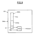
- a GMIx instruction comprises (FIG. 9) a useful field PUx representative of the actual content of the instruction, a CHGx field identifying the guard indication Gx, and an identification bit ID whose logical value means whether or not there is an instruction GMIx valid. More specifically, if the ID bit is 1 for example, this means that the GMIx instruction has not yet been processed by the EX stage.
- the MC2 command block therefore receives the bit as input. of identification ID and the bit BBx and delivers a logic signal DUGxV. If this logic signal is 0, this means that a GMIx instruction is always running. On the other hand, if the signal DUGxV is at 1, it means that this GMIx instruction has been executed and that the value of the indication guard Gx has been updated.
- the second MCTG production means include an RGV register containing the sixteen values of the DUGxV logic signals.
- the MCTG means also include logical means MLG, formed here by an AND logic gate and an inverter. These means first receive the first representative logic signal SL1x of the zero value or not of the counter CPTx, and on the other hand the second DUGxV logic signal from the RGV register.
- ET logic gate output provides second signal DEGxV flag associated with the GMIx instruction and whose control of the logical value will be carried out by the second means of control of validity MCV2, at the start of the current cycle during which the decoder DCD1 is preparing to receive the guarded connection instruction.
- the instruction of guarded connection may or may not be delivered and processed by the module BRU connection. If it is to be processed by the BRU connection, then the BRU connection module will use the value of the guard indication Gx contained in the duplicated register GRC (DEGx signal). Depending on this value, the connection instruction will actually be executed or not.
- the BRU connection module will use the value of the guard indication Gx contained in the duplicated register GRC (DEGx signal). Depending on this value, the connection instruction will actually be executed or not.
Landscapes
- Engineering & Computer Science (AREA)
- Software Systems (AREA)
- Theoretical Computer Science (AREA)
- Physics & Mathematics (AREA)
- General Engineering & Computer Science (AREA)
- General Physics & Mathematics (AREA)
- Executing Machine-Instructions (AREA)
- Advance Control (AREA)
Applications Claiming Priority (2)
| Application Number | Priority Date | Filing Date | Title |
|---|---|---|---|
| FR0102645 | 2001-02-27 | ||
| FR0102645A FR2821450B1 (fr) | 2001-02-27 | 2001-02-27 | Procede de gestion d'instructions de branchement au sein d'un processeur, en particulier un processeur de traitement numerique du signal, et processeur correspondant |
Publications (1)
| Publication Number | Publication Date |
|---|---|
| EP1235140A1 true EP1235140A1 (de) | 2002-08-28 |
Family
ID=8860491
Family Applications (1)
| Application Number | Title | Priority Date | Filing Date |
|---|---|---|---|
| EP02290402A Withdrawn EP1235140A1 (de) | 2001-02-27 | 2002-02-20 | Verfahren zur Verzweigungsverwaltung in einem Prozessor |
Country Status (3)
| Country | Link |
|---|---|
| US (1) | US7370182B2 (de) |
| EP (1) | EP1235140A1 (de) |
| FR (1) | FR2821450B1 (de) |
Families Citing this family (1)
| Publication number | Priority date | Publication date | Assignee | Title |
|---|---|---|---|---|
| US7849444B2 (en) * | 2004-12-21 | 2010-12-07 | National Instruments Corporation | Test executive with buffer overwrite detection for parameters of user-supplied code modules |
Citations (6)
| Publication number | Priority date | Publication date | Assignee | Title |
|---|---|---|---|---|
| EP0133477A2 (de) * | 1983-07-06 | 1985-02-27 | Nec Corporation | Pipeline gesteuertes Informationsverarbeitungssystem |
| US4827402A (en) * | 1985-04-22 | 1989-05-02 | Hitachi, Ltd. | Branch advanced control apparatus for advanced control of a branch instruction in a data processing system |
| EP0689131A1 (de) * | 1994-06-22 | 1995-12-27 | STMicroelectronics Limited | Rechnersystem zur Ausführung von Verzweigungsbefehlen |
| EP0840209A2 (de) * | 1996-11-01 | 1998-05-06 | Matsushita Electric Industrial Co., Ltd. | Verfahren und Vorrichtung zum Befehlsvorausholen |
| WO1999008184A1 (en) * | 1997-08-06 | 1999-02-18 | Advanced Micro Devices, Inc. | An apparatus and method for accessing special registers without serialization |
| EP1050805A1 (de) * | 1999-05-03 | 2000-11-08 | STMicroelectronics SA | Übertragung von Schutzwerten in einem Rechnersystem |
Family Cites Families (5)
| Publication number | Priority date | Publication date | Assignee | Title |
|---|---|---|---|---|
| JPH0820950B2 (ja) * | 1990-10-09 | 1996-03-04 | インターナショナル・ビジネス・マシーンズ・コーポレイション | マルチ予測型分岐予測機構 |
| JP2761688B2 (ja) * | 1992-02-07 | 1998-06-04 | 三菱電機株式会社 | データ処理装置 |
| US5928357A (en) * | 1994-09-15 | 1999-07-27 | Intel Corporation | Circuitry and method for performing branching without pipeline delay |
| US6189091B1 (en) * | 1998-12-02 | 2001-02-13 | Ip First, L.L.C. | Apparatus and method for speculatively updating global history and restoring same on branch misprediction detection |
| US6543002B1 (en) * | 1999-11-04 | 2003-04-01 | International Business Machines Corporation | Recovery from hang condition in a microprocessor |
-
2001
- 2001-02-27 FR FR0102645A patent/FR2821450B1/fr not_active Expired - Fee Related
-
2002
- 2002-02-20 EP EP02290402A patent/EP1235140A1/de not_active Withdrawn
- 2002-02-25 US US10/082,816 patent/US7370182B2/en active Active
Patent Citations (6)
| Publication number | Priority date | Publication date | Assignee | Title |
|---|---|---|---|---|
| EP0133477A2 (de) * | 1983-07-06 | 1985-02-27 | Nec Corporation | Pipeline gesteuertes Informationsverarbeitungssystem |
| US4827402A (en) * | 1985-04-22 | 1989-05-02 | Hitachi, Ltd. | Branch advanced control apparatus for advanced control of a branch instruction in a data processing system |
| EP0689131A1 (de) * | 1994-06-22 | 1995-12-27 | STMicroelectronics Limited | Rechnersystem zur Ausführung von Verzweigungsbefehlen |
| EP0840209A2 (de) * | 1996-11-01 | 1998-05-06 | Matsushita Electric Industrial Co., Ltd. | Verfahren und Vorrichtung zum Befehlsvorausholen |
| WO1999008184A1 (en) * | 1997-08-06 | 1999-02-18 | Advanced Micro Devices, Inc. | An apparatus and method for accessing special registers without serialization |
| EP1050805A1 (de) * | 1999-05-03 | 2000-11-08 | STMicroelectronics SA | Übertragung von Schutzwerten in einem Rechnersystem |
Non-Patent Citations (2)
| Title |
|---|
| MOORE C R: "THE POWERPCTM 601 MICROPROCESSOR", PROCEEDINGS OF THE SPRING COMPUTER SOCIETY INTERNATIONAL CONFERENCE. (COMPCON). SAN FRANCISCO, FEB. 22 - 26, 1993, LOS ALAMITOS, IEEE COMP. SOC. PRESS, US, vol. CONF. 38, 22 February 1993 (1993-02-22), pages 109 - 116, XP000379036, ISBN: 0-7803-1294-5 * |
| TOYOHIKO YOSHIDA ET AL: "A STRATEGY FOR AVOIDING PIPELINE INTERLOCK DELAYS IN A MICROPROCESSOR", PROCEEDINGS OF THE INTERNATIONAL CONFERENCE ON COMPUTER DESIGN: VLSI IN COMPUTERS AND PROCESSORS. CAMBRIDGE, MA., SEPT. 17 - 19, 1990, LOS ALAMITOS, IEE COMP. SOC. PRESS, US, 17 September 1990 (1990-09-17), pages 14 - 19, XP000201400, ISBN: 0-8186-2079-X * |
Also Published As
| Publication number | Publication date |
|---|---|
| FR2821450B1 (fr) | 2004-07-09 |
| US20020124044A1 (en) | 2002-09-05 |
| FR2821450A1 (fr) | 2002-08-30 |
| US7370182B2 (en) | 2008-05-06 |
Similar Documents
| Publication | Publication Date | Title |
|---|---|---|
| EP0434483B1 (de) | Prozessor mit mehreren mikroprogrammierten Ausführungseinheiten | |
| EP0030504A1 (de) | Vorrichtung zur Synchronisation und Zuteilung von Prozessen zwischen mehreren Verarbeitungseinheiten in einem Datenverarbeitungssystem | |
| FR2500659A1 (fr) | Dispositif pour l'allocation dynamique des taches d'un ordinateur multiprocesseur | |
| FR2632090A1 (fr) | Commande du fonctionnement en pipe-line d'un systeme de micro-calculateur utilisant le dimensionnement dynamique des bus avec un processeur 80386 et une unite de commande d'antememoire 82385 | |
| EP1027644B1 (de) | Mikroprozessor, insbesondere für chipkarte und befehlsverarbeitungsverfahren | |
| EP0392932B1 (de) | Verfahren und Vorrichtung zur Speicherzugriffsbeschleunigung unter Verwendung eines modifizierten LRU-Algorithmus | |
| FR2880963A1 (fr) | Points d'arrets logiciels destines a etre utilises avec des dispositifs a memoire | |
| FR3103585A1 (fr) | Procédé de gestion de la configuration d’accès à des périphériques et à leurs ressources associées d’un système sur puce formant par exemple un microcontrôleur, et système sur puce correspondant | |
| US6374338B1 (en) | Method for performing configuration tasks prior to and including memory configuration within a processor-based system | |
| FR3103584A1 (fr) | Procédé de gestion du débogage d’un système sur puce formant par exemple un microcontrôleur, et système sur puce correspondant | |
| EP1235140A1 (de) | Verfahren zur Verzweigungsverwaltung in einem Prozessor | |
| EP0435718A1 (de) | Prozessor mit mehreren mikroprogrammierten Einheiten und mit einem Mechanismus zur vorzeitigen Befehlsausführung | |
| FR2644912A1 (fr) | Controleur logique programmable et procede pour le faire fonctionner | |
| FR2821449A1 (fr) | Procede de gestion d'instructions au sein d'un processeur a architecture decouplee, en particulier un processeur de traitement numerique du signal, et processeur correspondant | |
| FR2778254A1 (fr) | Circuits,systemes et procedes d'ordinateur utilisant un nettoyage partiel d'une memoire cache | |
| FR2794259A1 (fr) | Dispositif materiel destine a l'execution d'instructions programmables basees sur des micro-instructions | |
| EP4187393A1 (de) | Dynamische verwaltung einer speicherfire | |
| EP0081873B1 (de) | Datenverarbeitungssystem das die Verwendung des selben Lösch- und Programmierspeichers erlaubt um Instruktionen und Daten sowohl zu lesen, als zu schreiben | |
| FR2871908A1 (fr) | Procede et programme d'ordinateur de traitement d'une adresse virtuelle pour la programmation d'un controleur de dma et systeme sur puce associe | |
| EP1235141A1 (de) | Verwaltungsverfahren für konditionierte Befehle in einem Prozessor, und Prozessor dafür | |
| EP0426531B1 (de) | Prüfsystem für einen Mikroprozessor | |
| FR2513778A1 (fr) | Dispositif et procede d'informatique | |
| EP1250645B1 (de) | Gerätetreibersystem in einer integrierten schaltung | |
| FR2662830A1 (fr) | Procede de dialogue entre les processeurs d'un systeme, systeme pour sa mise en óoeuvre et utilisation pour la repartition des processus aux processeurs. | |
| EP0733977A1 (de) | Rechnersystem mit hierarchischen Speichern |
Legal Events
| Date | Code | Title | Description |
|---|---|---|---|
| PUAI | Public reference made under article 153(3) epc to a published international application that has entered the european phase |
Free format text: ORIGINAL CODE: 0009012 |
|
| AK | Designated contracting states |
Kind code of ref document: A1 Designated state(s): AT BE CH CY DE DK ES FI FR GB GR IE IT LI LU MC NL PT SE TR |
|
| AX | Request for extension of the european patent |
Free format text: AL;LT;LV;MK;RO;SI |
|
| 17P | Request for examination filed |
Effective date: 20020905 |
|
| RIN1 | Information on inventor provided before grant (corrected) |
Inventor name: MERLANDE, ANNE Inventor name: FERROUSSAT, SEBASTIEN Inventor name: COFLER, ANDREW |
|
| AKX | Designation fees paid |
Designated state(s): DE FR GB IT |
|
| STAA | Information on the status of an ep patent application or granted ep patent |
Free format text: STATUS: THE APPLICATION IS DEEMED TO BE WITHDRAWN |
|
| 18D | Application deemed to be withdrawn |
Effective date: 20090901 |