EP1235109A1 - Method for exposing at least one or at least two semiconductor wafers - Google Patents
Method for exposing at least one or at least two semiconductor wafers Download PDFInfo
- Publication number
- EP1235109A1 EP1235109A1 EP01104358A EP01104358A EP1235109A1 EP 1235109 A1 EP1235109 A1 EP 1235109A1 EP 01104358 A EP01104358 A EP 01104358A EP 01104358 A EP01104358 A EP 01104358A EP 1235109 A1 EP1235109 A1 EP 1235109A1
- Authority
- EP
- European Patent Office
- Prior art keywords
- alignment
- parameters
- values
- tool
- overlay
- Prior art date
- Legal status (The legal status is an assumption and is not a legal conclusion. Google has not performed a legal analysis and makes no representation as to the accuracy of the status listed.)
- Withdrawn
Links
Images


Classifications
-
- G—PHYSICS
- G03—PHOTOGRAPHY; CINEMATOGRAPHY; ANALOGOUS TECHNIQUES USING WAVES OTHER THAN OPTICAL WAVES; ELECTROGRAPHY; HOLOGRAPHY
- G03F—PHOTOMECHANICAL PRODUCTION OF TEXTURED OR PATTERNED SURFACES, e.g. FOR PRINTING, FOR PROCESSING OF SEMICONDUCTOR DEVICES; MATERIALS THEREFOR; ORIGINALS THEREFOR; APPARATUS SPECIALLY ADAPTED THEREFOR
- G03F7/00—Photomechanical, e.g. photolithographic, production of textured or patterned surfaces, e.g. printing surfaces; Materials therefor, e.g. comprising photoresists; Apparatus specially adapted therefor
- G03F7/70—Microphotolithographic exposure; Apparatus therefor
- G03F7/70483—Information management; Active and passive control; Testing; Wafer monitoring, e.g. pattern monitoring
- G03F7/70605—Workpiece metrology
- G03F7/70616—Monitoring the printed patterns
- G03F7/70633—Overlay, i.e. relative alignment between patterns printed by separate exposures in different layers, or in the same layer in multiple exposures or stitching
-
- H—ELECTRICITY
- H10—SEMICONDUCTOR DEVICES; ELECTRIC SOLID-STATE DEVICES NOT OTHERWISE PROVIDED FOR
- H10P—GENERIC PROCESSES OR APPARATUS FOR THE MANUFACTURE OR TREATMENT OF DEVICES COVERED BY CLASS H10
- H10P76/00—Manufacture or treatment of masks on semiconductor bodies, e.g. by lithography or photolithography
-
- G—PHYSICS
- G03—PHOTOGRAPHY; CINEMATOGRAPHY; ANALOGOUS TECHNIQUES USING WAVES OTHER THAN OPTICAL WAVES; ELECTROGRAPHY; HOLOGRAPHY
- G03F—PHOTOMECHANICAL PRODUCTION OF TEXTURED OR PATTERNED SURFACES, e.g. FOR PRINTING, FOR PROCESSING OF SEMICONDUCTOR DEVICES; MATERIALS THEREFOR; ORIGINALS THEREFOR; APPARATUS SPECIALLY ADAPTED THEREFOR
- G03F9/00—Registration or positioning of originals, masks, frames, photographic sheets or textured or patterned surfaces, e.g. automatically
- G03F9/70—Registration or positioning of originals, masks, frames, photographic sheets or textured or patterned surfaces, e.g. automatically for microlithography
- G03F9/7003—Alignment type or strategy, e.g. leveling, global alignment
- G03F9/7046—Strategy, e.g. mark, sensor or wavelength selection
Definitions
- the present invention relates to a method for exposing at least two semiconductor wafers with a pattern, the exposure being performed in an exposure tool, an alignment being performed in response to a first set of alignment parameters, which depends on characteristics of each of said wafers, and a second set of alignment parameters, which accounts for an exposure tool-offset, and to a method for exposing at least one semiconductor wafer.
- process control is one of the main issues for providing high quality and efficiency of the device output of a manufacturing facility.
- process control is performed by measuring some characteristics of a group of wafers, e.g. a lot, after the wafers have been processed in a manufacturing tool.
- One example is measuring a critical dimension of semiconductor wafers in a lot after exposure.
- the lot is usually processed in a batch. Since processing tools and inspection tools are commonly grouped in different parts of a fab, wafers combined in a lot travel through the fab after the batch is finished with processing.
- the wafers of the lot are measured in an inspection tool and the measured characteristics may reveal problems with the processing tool, such as focus, alignment, coating or development problems in the case of wafers being processed in a lithographic cluster.
- problems can often be fixed by adjusting tool parameters, which are used to process wafers. Accordingly, having adjusted the processing tool setup using the inspection results as an input for correcting tool parameters, the next incoming batch or lot of semiconductor wafers can be processed with improved sets of tool parameters, resulting in an increased production yield.
- problems with single devices might not be covered, if, e.g., always just a first wafer in a lot is affected by a problem but it is not selected for inspection by statistical sampling. In this case the origin of a paramater drift in a process tool might not be recognized, or tool parameters might be adjusted inappropriately in reaction to a measured parameter drift. Thus, expensive process tool capacity is wasted and the time to manufacture a device is disadvantageously increased.
- the objective is solved by a method for exposing at least two semiconductor wafers with a pattern, the exposure being performed in an exposure tool, an alignment being performed in response to a first set of alignment parameters, which depend on characteristics of each of said wafers, and a second set of alignment parameters, which account for an exposure tool-offset, comprising the steps of providing a first semiconductor wafer to said exposure tool for exposing said wafer, performing alignment of said first semiconductor wafer, with determining values for said first set of alignment parameters, exposing the first semiconductor wafer using the combination of said first and second sets of alignment parameters, determining values for a set of parameters representing the overlay accuracy of said first pattern on said first semiconductor wafer, adjusting values of said second set of alignment parameters to correct for an overlay inaccuracy of said pattern, exposing a semiconductor wafer including an alignment in response to said adjusted values.
- the overlay measurement results of a first semiconductor wafer which can be determined in several ways, are used to change the tool parameter setup for the following or any other second wafer in a batch.
- the alignment is performed using two sets of alignment parameters.
- the first set of alignment parameters describes the way, in which an individual wafer is aligned and how the grid of exposure fields is set on the wafer. Examples of such parameters are the chip magnification, shifts in x- and y-direction, grid scaling in x- and y-direction, orthogonality of x- and y-direction, chip rotation, etc. These parameters are used for wafer steppers and scanners, whereby in the case of scanners the chip magnification is adjustable in x- and y-direction separately. Such parameters are determined during an alignment prior to any exposure of a wafer.
- the same parameters but with different values build up the second set of alignment parameters, which accounts for the exposure tool-offset.
- These offset values are each added to or subtracted from the corresponding parameters of the first set of alignment parameters after the values of said first set have been determined.
- These tool-offset parameters are used to correct for misalignments during the alignment of the semiconductor wafer.
- the quality of the alignment performance can be checked.
- sets of parameters representing the overlay accuracy can be related to sets of alignment parameters. Therefore, according to the present invention the second set of tool-offset alignment parameters is adjusted in its values to correct for an overlay inaccuracy of the pattern that either has been exposed or is to be exposed in case that the overlay data reveal values beyond a tolerance level.
- the objective can further be solved using a similar method, where the tool-offset parameters can be adjusted using already at least one semiconductor wafer. With each further wafer that is aligned and optionally exposed, the tool-offset parameters can even be further refined.
- the corrected tool-offset parameters necessarily will lead directly to an improved tool-setup, due to which the yield is advantageously increased.
- the method according to the present invention may be combined with a method similar to the advanced process control in the sense that the present method may be repeated a few times until there repeatedly is no adjustment of the values of the second set of alignment parameters necessary, after which the determination step for the values of the set of parameters representing the overlay accuracy can be skipped.
- the application of the method of the present invention leads to a situation, where costs can be saved due to a reduced amount of inspection time for wafers after exposure.
- the increased yield advantageously leads to a decreased throughput time.
- the case of calculating the parameters reflecting the overlay accuracy using a formula and adjusting the second set of alignment parameters, i.e. the tool-offset alignment parameters, is each performed prior to exposing the semiconductor wafer.
- This aspect of the method according to the present invention has the advantage, that the wafer is not exposed, until the sets of alignment parameters are arranged with values, that provide sufficient quality for the eventual exposure. Therefore, the yield is still further increased, the throughput time even further decreased and the costs are advantageously reduced.
- the step of determining the values for the set of parameters representing the overlay accuracy is considered to be performed by calculating the values from those alignment parameters, that have been determined in the exposure tool alignment, i.e. the first set of alignment parameters.
- This calculation can be based on the fact, that an overlay parameter measured with an inspection tool can as well be derived or calculated with a mathematical formula comprising a combination of alignment parameters of the first set, each of them being supplied with a coefficient, which depends on the exposure tool.
- This determination is found to recover a sample of measurements of corresponding overlay parameters to a high degree of accuracy.
- the coefficients have to be determined once for a complete tool-offset and can then be reused until the next complete setup of the corresponding exposure tool is performed. Typically, this is a duration of weeks or months.
- the overlay parameters are known immediately after the alignment in the exposure tool when the determination of the corresponding alignment parameters is finished. This preferentially happens by means of an alignment measurement. Since the values for the set of overlay parameters are known from the calculation, a measurement with an inspection tool can be skipped resulting in a further reduced wafer throughput time.
- the second set of alignment parameters i.e. the tool-offset alignment parameters are then adjusted according to the set of calculated overlay parameters.
- the mathematical formular for calculating the values of the set of parameters representing the overlay accuracy is considered to be a linear function with the coefficient in front of each alignment parameter being dependent on the exposure tool employed. A high degree of accuracy for recovering the overlay measurement results with a linear function is found, resulting in an easy and straightforward calculation step. Only a few coefficients are involved in this case.
- the stopping of the batch queue as a result of values for the set of the parameters representing the overlay accuracy exceeding threshold values corresponding to tolerance levels is considered.
- system maintenance can be conducted in response to a warning signal, that has been issued in this case.
- After having reset said exposure tool processing of semiconductor wafers can be continued.
- a second determination of the values of the set of parameters representing the overlay accuracy of the wafer pattern is considered.
- a warning signal is issued, when one of the parameters of the set of parameters representing the overlay accuracy of the pattern increases beyond a pre-determined tolerance level.
- each of the at least two semiconductor wafers is processed in a next manufacturing step after exposure without being inspected in an overlay tool.
- the values for the set of tool-offset alignment parameters are calculated from the set of parameters representing the overlay accuracy using a linear formula. This feature provides a fast feedback for the alignment procedure from the overlay parameter determination.
- a neuronal network is built by means of the results of the calculation of the values for the set of parameters representing the overlay accuracy performed by a control unit 100 in comparison with the measurement of the values for the set of parameters representing the overlay accuracy in the inspection tool 40, for adjusting the formula for calculating said values for the set of parameters representing the overlay accuracy.
- FIG. 1 The control of the wafer flow through processing steps 20, 30, 40, 90 according to an embodiment of the method of the present invention is shown in figure 1.
- thick arrows denote the physical wafer flow
- narrow arrows denote a flow of information, either signal and/or the data corresponding to the sets of alignment parameters.
- a semiconductor wafer batch queue 10 is provided for exposure. Prior to being exposed in an exposure step 30 a first semiconductor wafer 1 of the batch undergoes an alignment step 20 on the wafer stage inside the exposure tool 35.
- the wafer alignment parameter data which are measured during the alignment step 20, are examined in a control unit 100. Thereby, using the wafer alignment parameter data it calculates the relevant inspection overlay data, i.e. values for the set of overlay parameters representing the overlay accuracy of the pattern that is structured on the first semiconductor wafer 1.
- chip_mag (overlay) denotes the chip magnification as a parameter representing the overlay accuracy
- chip_mag (align) denotes the chip magnification as a wafer alignment parameter as determined during the alignment step
- scale_x and scale_y denote the grid scaling in x- and y-direction, respectively.
- the coefficients 1.24, 0.50 and 0.50 are exposure tool-dependent and are fixed for the duration of a typical tool setup.
- the calculated overlay parameter values are then compared each with parameter dependent tolerance levels according to the overlay accuracy specification provided for the product. If one the one side the calculated overlay data provide sufficient results, i.e. within a tolerance range, the wafer is forwarded to the next process step 90. On the other side if the overlay data reveal calculated values that increase beyond said tolerance levels, the wafer is forwarded to an inspection tool 40 for performing a second determination of the overlay parameters, i.e. a measurement. If this measurement actually reveals insufficient overlay quality the wafer is sent into rework 50, while it can be forwarded to the next process step 90 in case the overlay measurement reveals oppositely sufficient overlay accuracy.
- control unit 100 for determining the values for the set of overlay parameters from the values of the set of wafer alignment parameters might be appropriate.
- the new alignment offset can be determined by control unit 100 according to measurement results of the inspection tool 40 as described below.
- While a warning signal 105 is issued by the control unit 100 for controlling the further processing of the semiconductor wafer 1 as described above, also adjusted values for the set of tool-offset parameters are determined by control unit 100 for the alignment procedure. These values are to be added to the values of the set of wafer alignment parameters that are determined during the alignment step 20.
- a second semiconductor wafer 2 is then aligned and exposed in the exposure tool 35 using the adjusted tool-offset parameter values as indicated by the dashed line in the exposure unit 30 of figure 1, that correct for a possible misalignment derived by control unit 100 for the first semiconductor wafer 1.
- the alignment data may also be received by the control unit 100 prior to exposure, but the feedback to the alignment step 20 is only provided for the alignment of the following second semiconductor wafer 2.
- the exposure of the first semiconductor 1 is performed using the originally given values for the set of tool-offset alignment parameters (the first set of alignment parameters).
- FIG 2. Another embodiment of the present invention is shown in figure 2. It deviates from the embodiment shown in figure 1 by a closed loop feedback from control unit 100, which performs the wafer alignment parameter determination, the overlay parameter calculation and the tool-offset parameter adjustment already after the alignment 20 prior to wafer being exposed in exposure step 30.
- Semiconductor wafer 1 is aligned, while values for the alignment parameters are received by control unit 100.
- control unit 100 calculates values for the set of overlay parameters representing the overlay accuracy. Because the semiconductor wafer 1 is not yet exposed and still performing the alignment step 20, the tool-offset alignment parameters can be adjusted in-situ in case the overlay accuracy - and thus the tool-offset - can still be improved for the same first semiconductor wafer 1.
- an overlay control can optionally be issued by means of statistical process control (SPC) 101 for performing a statistical verification of the overlay results calculated due to the control unit 100.
- SPC statistical process control
- FIG. 3 A comparison of the method according to the present invention with prior art is indicated in figures 3 - 5.
- the tool-offset parameter for chip magnification is derived using wafer alignment parameters like grid scale in x- and y-direction as input for the calculation.
- the grid scaling in both directions for a measurement period of several wafers during a period 3 months is shown in figure 3. There, it can easily be seen, that e.g. the grid scaling in y-direction is scattering around each of the two distinct values of about 1.3 and 3 ppm.
- the altering grid scaling expressed as an alignment parameter has an influence on the chip magnification expressed as a parameter representing the overlay accuracy. Therefore, the chip magnification - this time expressed as an alignment parameter - can be provided with an offset to correct for the jumps in the grid scaling data.
- the corresponding tool-offsets that have been used to provide a conventionally optimum overlay accuracy, are displayed as diamonds. They were fixed at five distinct values for the tool-offset alignment parameter chip magnification, which were: initially 1.3 ppm, then 2 ppm, followed by 1 ppm, followed by 3 ppm and finally 1.9 ppm during the same period of 3 months, and for the same exposure tool and wafers as in figure 3.
- the corresponding diamonds reveal the final outcome for the overlay accuracy with respect to chip magnification.
- This prior art case is characterized by a large scatter between +2 ppm and -2 ppm in chip magnification.
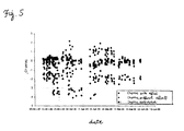
- the distinctly set tool-offset parameter chip magnification (diamonds in figure 4) provided a linear shift (offset) in figure 5 from the data represented by the circles, which represent the measured chip magnification overlay parameter as being measured without an offset applied during the alignment.
- the distinctly set offset parameters shifted the measured overlay data advantageously into the tolerance window for overlay, which, e.g., may be represented by a range for chip magnification between -1 ppm and +1 ppm.
- this handset chip magnification offset cannot impede the large scatter that is obvious from figure 5 from the diamonds as well as the circles.
- the amount of rework therefore is disadvantageously large.
- the tool-offset parameter chip magnification may be calculated individually for each wafer.
- the coefficients 4.21, 0.44 and 0.55 have been determined previously in the context of a change of the tool setup, e.g. after a maintenance.
- the ideal offset calculated using this formula is displayed as a set of squares in figure 4.
Landscapes
- Physics & Mathematics (AREA)
- General Physics & Mathematics (AREA)
- Exposure And Positioning Against Photoresist Photosensitive Materials (AREA)
- Exposure Of Semiconductors, Excluding Electron Or Ion Beam Exposure (AREA)
Abstract
Semiconductor wafers (1, 2), e.g. a lot (10), are exposed
after an alignment (20) in a wafer stepper or scanner (35)
with each determining their alignment parameters. Using,
e.g., a linear formula with tool specific coefficients the
overlay accuracy can be calculated from these alignment
parameters in advance to a high degree of accuracy as if a
measurement with an overlay inspection tool (40) had been
performed. The exposure tool-offset can be adjusted on a
wafer-to-wafer basis to correct for the overlay inaccuracy
derived. Moreover, the alignment parameters for a specific
wafer can be used to change the tool-offset for the same
wafer prior to exposure. The required inspection tool (40)
capacity is advantageously reduced, the wafer rework decreases
and time is saved to perform the exposure step (30).
Description
- The present invention relates to a method for exposing at least two semiconductor wafers with a pattern, the exposure being performed in an exposure tool, an alignment being performed in response to a first set of alignment parameters, which depends on characteristics of each of said wafers, and a second set of alignment parameters, which accounts for an exposure tool-offset, and to a method for exposing at least one semiconductor wafer.
- In semiconductor wafer manufacturing the tool and process control is one of the main issues for providing high quality and efficiency of the device output of a manufacturing facility. Typically, process control is performed by measuring some characteristics of a group of wafers, e.g. a lot, after the wafers have been processed in a manufacturing tool. One example is measuring a critical dimension of semiconductor wafers in a lot after exposure. The lot is usually processed in a batch. Since processing tools and inspection tools are commonly grouped in different parts of a fab, wafers combined in a lot travel through the fab after the batch is finished with processing. Eventually, the wafers of the lot are measured in an inspection tool and the measured characteristics may reveal problems with the processing tool, such as focus, alignment, coating or development problems in the case of wafers being processed in a lithographic cluster. These problems can often be fixed by adjusting tool parameters, which are used to process wafers. Accordingly, having adjusted the processing tool setup using the inspection results as an input for correcting tool parameters, the next incoming batch or lot of semiconductor wafers can be processed with improved sets of tool parameters, resulting in an increased production yield.
- Usually these measurements in an inspection tool are based on dynamic or static sampling. Typically, not every device in a batch is controlled, rather statistical methods are used to pick out a subsample of the lot for the measurement and the results are feeded back for the new incoming batch devices, which are to be processed. Thereby, it is assumed that the next incoming batch devices being manufactured with improved tool parameters behave in the same manner as the previous batch with respect to the tool parameters, which might not always be the case.
- Using this conventional method of statistical process control (SPC) several further disadvantages arise. One is that processed wafers of a batch or lot, that have selectively just been measured in an inspection tool indicating problems with the process tool setup, all have to be moved into rework because they are each most probably affected by these problems. Therefore, free inspection tool capacity as well as the throughput and yield of the process tool are disadvantageously reduced.
- Furthermore, problems with single devices might not be covered, if, e.g., always just a first wafer in a lot is affected by a problem but it is not selected for inspection by statistical sampling. In this case the origin of a paramater drift in a process tool might not be recognized, or tool parameters might be adjusted inappropriately in reaction to a measured parameter drift. Thus, expensive process tool capacity is wasted and the time to manufacture a device is disadvantageously increased.
- It is therefore a primary objective of the present invention to accelerate the throughput of lots or batches of semiconductor wafers in a process tool, to increase the wafer yield and to save costs in semiconductor wafer manufacturing.
- The objective is solved by a method for exposing at least two semiconductor wafers with a pattern, the exposure being performed in an exposure tool, an alignment being performed in response to a first set of alignment parameters, which depend on characteristics of each of said wafers, and a second set of alignment parameters, which account for an exposure tool-offset, comprising the steps of providing a first semiconductor wafer to said exposure tool for exposing said wafer, performing alignment of said first semiconductor wafer, with determining values for said first set of alignment parameters, exposing the first semiconductor wafer using the combination of said first and second sets of alignment parameters, determining values for a set of parameters representing the overlay accuracy of said first pattern on said first semiconductor wafer, adjusting values of said second set of alignment parameters to correct for an overlay inaccuracy of said pattern, exposing a semiconductor wafer including an alignment in response to said adjusted values.
- Using the method according to the present invention the overlay measurement results of a first semiconductor wafer, which can be determined in several ways, are used to change the tool parameter setup for the following or any other second wafer in a batch. In the context of this invention the alignment is performed using two sets of alignment parameters. The first set of alignment parameters describes the way, in which an individual wafer is aligned and how the grid of exposure fields is set on the wafer. Examples of such parameters are the chip magnification, shifts in x- and y-direction, grid scaling in x- and y-direction, orthogonality of x- and y-direction, chip rotation, etc. These parameters are used for wafer steppers and scanners, whereby in the case of scanners the chip magnification is adjustable in x- and y-direction separately. Such parameters are determined during an alignment prior to any exposure of a wafer.
- The same parameters but with different values build up the second set of alignment parameters, which accounts for the exposure tool-offset. These offset values are each added to or subtracted from the corresponding parameters of the first set of alignment parameters after the values of said first set have been determined. These tool-offset parameters are used to correct for misalignments during the alignment of the semiconductor wafer.
- Having determined the values for a set of alignment parameters representing the overlay accuracy of the pattern on the first semiconductor wafer, that just has been exposed or is to be exposed in the exposure tool, the quality of the alignment performance can be checked. Generally, sets of parameters representing the overlay accuracy can be related to sets of alignment parameters. Therefore, according to the present invention the second set of tool-offset alignment parameters is adjusted in its values to correct for an overlay inaccuracy of the pattern that either has been exposed or is to be exposed in case that the overlay data reveal values beyond a tolerance level.
- The objective can further be solved using a similar method, where the tool-offset parameters can be adjusted using already at least one semiconductor wafer. With each further wafer that is aligned and optionally exposed, the tool-offset parameters can even be further refined. The corrected tool-offset parameters necessarily will lead directly to an improved tool-setup, due to which the yield is advantageously increased. Moreover, the method according to the present invention may be combined with a method similar to the advanced process control in the sense that the present method may be repeated a few times until there repeatedly is no adjustment of the values of the second set of alignment parameters necessary, after which the determination step for the values of the set of parameters representing the overlay accuracy can be skipped. Thus, the application of the method of the present invention leads to a situation, where costs can be saved due to a reduced amount of inspection time for wafers after exposure. Furthermore, the increased yield advantageously leads to a decreased throughput time.
- In a another aspect of the present invention the case of calculating the parameters reflecting the overlay accuracy using a formula and adjusting the second set of alignment parameters, i.e. the tool-offset alignment parameters, is each performed prior to exposing the semiconductor wafer. This aspect of the method according to the present invention has the advantage, that the wafer is not exposed, until the sets of alignment parameters are arranged with values, that provide sufficient quality for the eventual exposure. Therefore, the yield is still further increased, the throughput time even further decreased and the costs are advantageously reduced.
- In a further aspect the step of determining the values for the set of parameters representing the overlay accuracy is considered to be performed by calculating the values from those alignment parameters, that have been determined in the exposure tool alignment, i.e. the first set of alignment parameters. This calculation can be based on the fact, that an overlay parameter measured with an inspection tool can as well be derived or calculated with a mathematical formula comprising a combination of alignment parameters of the first set, each of them being supplied with a coefficient, which depends on the exposure tool. This determination is found to recover a sample of measurements of corresponding overlay parameters to a high degree of accuracy. The coefficients have to be determined once for a complete tool-offset and can then be reused until the next complete setup of the corresponding exposure tool is performed. Typically, this is a duration of weeks or months.
- Therefore, the overlay parameters are known immediately after the alignment in the exposure tool when the determination of the corresponding alignment parameters is finished. This preferentially happens by means of an alignment measurement. Since the values for the set of overlay parameters are known from the calculation, a measurement with an inspection tool can be skipped resulting in a further reduced wafer throughput time. The second set of alignment parameters, i.e. the tool-offset alignment parameters are then adjusted according to the set of calculated overlay parameters.
- In a further aspect the mathematical formular for calculating the values of the set of parameters representing the overlay accuracy is considered to be a linear function with the coefficient in front of each alignment parameter being dependent on the exposure tool employed. A high degree of accuracy for recovering the overlay measurement results with a linear function is found, resulting in an easy and straightforward calculation step. Only a few coefficients are involved in this case.
- In a further aspect the stopping of the batch queue as a result of values for the set of the parameters representing the overlay accuracy exceeding threshold values corresponding to tolerance levels is considered. After the batch or lot processing is stopped system maintenance can be conducted in response to a warning signal, that has been issued in this case. After having reset said exposure tool processing of semiconductor wafers can be continued.
- In a further aspect a second determination of the values of the set of parameters representing the overlay accuracy of the wafer pattern is considered. A warning signal is issued, when one of the parameters of the set of parameters representing the overlay accuracy of the pattern increases beyond a pre-determined tolerance level. A detailed investigation of the parameters and the reason why the tolerance level has been exceeded, can than be performed by remeasuring values of the overlay parameters, which priorily have been calculated using the formular from the first set of alignment parameters.
- In a further aspect it is considered that each of the at least two semiconductor wafers is processed in a next manufacturing step after exposure without being inspected in an overlay tool.
- In a further aspect it is considered, that also the values for the set of tool-offset alignment parameters are calculated from the set of parameters representing the overlay accuracy using a linear formula. This feature provides a fast feedback for the alignment procedure from the overlay parameter determination.
- In a furhter aspect, a neuronal network is built by means of the results of the calculation of the values for the set of parameters representing the overlay accuracy performed by a
control unit 100 in comparison with the measurement of the values for the set of parameters representing the overlay accuracy in theinspection tool 40, for adjusting the formula for calculating said values for the set of parameters representing the overlay accuracy. - The invention will be better understood by reference to the following description of embodiments of the invention taken in conjunction with the accompanying drawings, wherein
- figure 1
- schematically shows the wafer process flow in lithography as well as the alignment feedback according to an embodiment of the present invention,
- figure 2
- displays the same as in figure 1, but for an embodiment comprising an offset adjustment prior to exposure according to the present invention,
- figure 3
- displays a diagram of grid scale data in x- and y-direction measured as a wafer alignment parameter during an alignment for the exposure of DRAM wafers within a period of 3 months versus exposure date,
- figure 4
- shows a diagram with used values for the tool-offset parameter chip magnification according to prior art (diamonds) versus date, overplotted with calculated offset values (squares) for the same parameter according to an embodiment of the present invention, for the exposure of the same DRAM wafers as displayed in figure 3,
- figure 5
- shows a plot of the overlay parameter chip magnification representing the overlay accuracy of a pattern as measured with an KLA overlay inspection tool, with and without applied tool-offset (diamonds and circles, resp.) according to prior art, and as being calculated (squares) according to an embodiment of the present invention, for the same DRAM wafers as displayed in figure 3, versus date.
- The control of the wafer flow through processing steps 20, 30, 40, 90 according to an embodiment of the method of the present invention is shown in figure 1. There, thick arrows denote the physical wafer flow, while narrow arrows denote a flow of information, either signal and/or the data corresponding to the sets of alignment parameters. A semiconductor
wafer batch queue 10 is provided for exposure. Prior to being exposed in an exposure step 30 afirst semiconductor wafer 1 of the batch undergoes analignment step 20 on the wafer stage inside theexposure tool 35. - After the wafer has been exposed the wafer alignment parameter data, which are measured during the
alignment step 20, are examined in acontrol unit 100. Thereby, using the wafer alignment parameter data it calculates the relevant inspection overlay data, i.e. values for the set of overlay parameters representing the overlay accuracy of the pattern that is structured on thefirst semiconductor wafer 1. - For example, the chip magnification expressed as an overlay parameter is calculated using a linear formula
- The calculated overlay parameter values are then compared each with parameter dependent tolerance levels according to the overlay accuracy specification provided for the product. If one the one side the calculated overlay data provide sufficient results, i.e. within a tolerance range, the wafer is forwarded to the
next process step 90. On the other side if the overlay data reveal calculated values that increase beyond said tolerance levels, the wafer is forwarded to aninspection tool 40 for performing a second determination of the overlay parameters, i.e. a measurement. If this measurement actually reveals insufficient overlay quality the wafer is sent intorework 50, while it can be forwarded to thenext process step 90 in case the overlay measurement reveals oppositely sufficient overlay accuracy. In the latter case a re-determination of the calculation formula used incontrol unit 100 for determining the values for the set of overlay parameters from the values of the set of wafer alignment parameters might be appropriate. Nevertheless, the new alignment offset can be determined bycontrol unit 100 according to measurement results of theinspection tool 40 as described below. - While a
warning signal 105 is issued by thecontrol unit 100 for controlling the further processing of thesemiconductor wafer 1 as described above, also adjusted values for the set of tool-offset parameters are determined bycontrol unit 100 for the alignment procedure. These values are to be added to the values of the set of wafer alignment parameters that are determined during thealignment step 20. Asecond semiconductor wafer 2 is then aligned and exposed in theexposure tool 35 using the adjusted tool-offset parameter values as indicated by the dashed line in theexposure unit 30 of figure 1, that correct for a possible misalignment derived bycontrol unit 100 for thefirst semiconductor wafer 1. The alignment data may also be received by thecontrol unit 100 prior to exposure, but the feedback to thealignment step 20 is only provided for the alignment of the followingsecond semiconductor wafer 2. The exposure of thefirst semiconductor 1 is performed using the originally given values for the set of tool-offset alignment parameters (the first set of alignment parameters). - Another embodiment of the present invention is shown in figure 2. It deviates from the embodiment shown in figure 1 by a closed loop feedback from
control unit 100, which performs the wafer alignment parameter determination, the overlay parameter calculation and the tool-offset parameter adjustment already after thealignment 20 prior to wafer being exposed inexposure step 30.Semiconductor wafer 1 is aligned, while values for the alignment parameters are received bycontrol unit 100. As in the previousembodiment control unit 100 then calculates values for the set of overlay parameters representing the overlay accuracy. Because thesemiconductor wafer 1 is not yet exposed and still performing thealignment step 20, the tool-offset alignment parameters can be adjusted in-situ in case the overlay accuracy - and thus the tool-offset - can still be improved for the samefirst semiconductor wafer 1. - After being exposed an overlay control can optionally be issued by means of statistical process control (SPC) 101 for performing a statistical verification of the overlay results calculated due to the
control unit 100. - A comparison of the method according to the present invention with prior art is indicated in figures 3 - 5. As an example the tool-offset parameter for chip magnification is derived using wafer alignment parameters like grid scale in x- and y-direction as input for the calculation. The grid scaling in both directions for a measurement period of several wafers during a period 3 months is shown in figure 3. There, it can easily be seen, that e.g. the grid scaling in y-direction is scattering around each of the two distinct values of about 1.3 and 3 ppm.
- It has been found, that the altering grid scaling expressed as an alignment parameter has an influence on the chip magnification expressed as a parameter representing the overlay accuracy. Therefore, the chip magnification - this time expressed as an alignment parameter - can be provided with an offset to correct for the jumps in the grid scaling data.
In figure 4 the corresponding tool-offsets, that have been used to provide a conventionally optimum overlay accuracy, are displayed as diamonds. They were fixed at five distinct values for the tool-offset alignment parameter chip magnification, which were: initially 1.3 ppm, then 2 ppm, followed by 1 ppm, followed by 3 ppm and finally 1.9 ppm during the same period of 3 months, and for the same exposure tool and wafers as in figure 3. - In figure 5 the corresponding diamonds reveal the final outcome for the overlay accuracy with respect to chip magnification. This prior art case is characterized by a large scatter between +2 ppm and -2 ppm in chip magnification. The distinctly set tool-offset parameter chip magnification (diamonds in figure 4) provided a linear shift (offset) in figure 5 from the data represented by the circles, which represent the measured chip magnification overlay parameter as being measured without an offset applied during the alignment. Thus, the distinctly set offset parameters shifted the measured overlay data advantageously into the tolerance window for overlay, which, e.g., may be represented by a range for chip magnification between -1 ppm and +1 ppm. But this handset chip magnification offset cannot impede the large scatter that is obvious from figure 5 from the diamonds as well as the circles. In this prior art case, the amount of rework therefore is disadvantageously large.
- Using the embodiment of the present invention, e.g. according to figure 2, the tool-offset parameter chip magnification may be calculated individually for each wafer. A linear formula is used, given by
- The ideal offset calculated using this formula is displayed as a set of squares in figure 4. The data scatter around the conventionally derived tool-offset chip magnification. But because this scatter originates from a correction of the scatter in the chip magnification overlay data, the quality of the overlay results has strongly increased as can be seen by the squares in figure 5. All values for the overlay chip magnification are within the tolerance level of -1 ppm to +1 ppm. Thus, the yield is advantageously increased and the throughput time efficiently reduced. Moreover, free inspection tool capacity is gained, since the overlay control in most cases can be skipped using the method according to the present invention.
-
- 1
- first semiconductor wafer
- 2
- second semiconductor wafer
- 10
- batch or lot of wafers
- 20
- alignment
- 30
- exposure step
- 35
- exposure tool
- 40
- overlay inspection
- 50
- rework
- 90
- next process step
- 100
- control unit
- 101
- statistical process control
- 105
- warning signal
Claims (8)
- Method for exposing at least two semiconductor wafers (1, 2) with a pattern, the exposure being performed in an exposure tool (35), an alignment (20) being performed in response to a first set of alignment parameters, which depends on characteristics of each of said wafers (1, 2), and a second set of alignment parameters, which accounts for an exposure tool-offset, comprising the steps of:i) providing a first semiconductor wafer (1) to said exposure tool (35) for exposing said wafer,ii) performing an alignment (20) of said first semiconductor wafer (1), with determining values for said first set of alignment parameters,iii) exposing the first semiconductor wafer using a combination of said first and second sets of alignment parameters,iv) calculating the values for a set of parameters representing the overlay accuracy of said first pattern on said first semiconductor wafer (1) from said first set of alignment parameters,v) adjusting values of said second set of alignment parameters to correct for an overlay inaccuracy of said pattern,vi) exposing said second semiconductor wafer (2) including an alignment (20) in response to said adjusted values.
- Method for exposing at least one semiconductor wafer (1) with a pattern, the exposure being performed in an exposure tool (35), an alignment being performed in response to a first set of alignment parameters, which depends on characteristics of each of said wafers, and a second set of alignment parameters, which accounts for an exposure tool-offset, comprising the steps of:i) providing said at least one semiconductor wafer (1) to said exposure tool (35) for exposing said wafer,ii) performing an alignment (20) of said at least one semiconductor wafer, with determining values for said first set of alignment parameters,iii) calculating values for a set of parameters representing the overlay accuracy of said pattern on said at least one semiconductor wafer (1) from said first set of alignment parameters,iv) adjusting values of said second set of alignment parameters to correct for an overlay inaccuracy of said pattern,v) exposing said at least one semiconductor wafer (1) including an alignment (20) in response to said adjustment using a combination of said first and second sets of alignment parameters for the wafer alignment.
- Method according to claims 1 or 2,
characterized in that
a formula is used to calculate said values of said set of parameters representing the overlay accuracy, which is a linear function with coefficients for each alignment parameter. - Method according to anyone of claims 1, 2 or 3,
characterized byissuing a warning signal (105), when one of the parameters of said set of parameters representing the overlay accuracy of said pattern increases beyond a predetermined tolerance level,stopping the processing with said exposure tool (35) for conducting system maintenance in response to said warning signal (105),continuing with processing after resetting said exposure tool (35). - Method according to anyone of claims 1, 2 or 3,
characterized byissuing a warning signal (105), when one of the parameters of said set of parameters representing the overlay accuracy of said pattern increases beyond a predetermined tolerance level,said set of parameters reflecting the overlay accuracy of said pattern on said semiconductor wafer is derived for a second time by measuring the parameters with an overlay inspection tool (40) after the semiconductor wafer (1) has been exposed with said pattern. - Method according to anyone of claims 1 to 5,
characterized in that
each semiconductor wafer is processed in a next manufacturing step after exposure (30) without being inspected in an overlay inspection tool (40). - Method according to anyone of claims 1 to 6,
characterized in that
the adjustment step for the values of said second set of alignment parameters is performed by calculating the values of said second set of alignment parameters from the values of said set of parameters representing the overlay accuracy using a formula, which is a linear function with coefficients for each alignment parameter. - Method according to anyone of claims 3 to 7,
characterized in that
a neuronal network is built by means of the results of the calculation of the values for the set of parameters representing the overlay accuracy performed by a control unit (100) in comparison with the measurement of the values for the set of parameters representing the overlay accuracy in the inspection tool (40), for adjusting the formula for calculating said values for the set of parameters representing the overlay accuracy.
Priority Applications (7)
| Application Number | Priority Date | Filing Date | Title |
|---|---|---|---|
| EP01104358A EP1235109A1 (en) | 2001-02-23 | 2001-02-23 | Method for exposing at least one or at least two semiconductor wafers |
| TW091103166A TW557490B (en) | 2001-02-23 | 2002-02-22 | Method for exposing at least one or at least two semiconductor wafers |
| KR1020037011002A KR100549054B1 (en) | 2001-02-23 | 2002-02-25 | How to expose one or more semiconductor wafers |
| JP2002568104A JP4117195B2 (en) | 2001-02-23 | 2002-02-25 | Method for exposing at least one or two semiconductor wafers |
| PCT/EP2002/002029 WO2002069047A1 (en) | 2001-02-23 | 2002-02-25 | Method for exposing at least one or at least two semiconductor wafers |
| EP02722139A EP1362261A1 (en) | 2001-02-23 | 2002-02-25 | Method for exposing at least one or at least two semiconductor wafers |
| US10/635,583 US6979522B2 (en) | 2001-02-23 | 2003-08-06 | Method for exposing at least one or at least two semiconductor wafers |
Applications Claiming Priority (1)
| Application Number | Priority Date | Filing Date | Title |
|---|---|---|---|
| EP01104358A EP1235109A1 (en) | 2001-02-23 | 2001-02-23 | Method for exposing at least one or at least two semiconductor wafers |
Publications (1)
| Publication Number | Publication Date |
|---|---|
| EP1235109A1 true EP1235109A1 (en) | 2002-08-28 |
Family
ID=8176572
Family Applications (2)
| Application Number | Title | Priority Date | Filing Date |
|---|---|---|---|
| EP01104358A Withdrawn EP1235109A1 (en) | 2001-02-23 | 2001-02-23 | Method for exposing at least one or at least two semiconductor wafers |
| EP02722139A Withdrawn EP1362261A1 (en) | 2001-02-23 | 2002-02-25 | Method for exposing at least one or at least two semiconductor wafers |
Family Applications After (1)
| Application Number | Title | Priority Date | Filing Date |
|---|---|---|---|
| EP02722139A Withdrawn EP1362261A1 (en) | 2001-02-23 | 2002-02-25 | Method for exposing at least one or at least two semiconductor wafers |
Country Status (6)
| Country | Link |
|---|---|
| US (1) | US6979522B2 (en) |
| EP (2) | EP1235109A1 (en) |
| JP (1) | JP4117195B2 (en) |
| KR (1) | KR100549054B1 (en) |
| TW (1) | TW557490B (en) |
| WO (1) | WO2002069047A1 (en) |
Cited By (2)
| Publication number | Priority date | Publication date | Assignee | Title |
|---|---|---|---|---|
| CN105223785A (en) * | 2015-10-30 | 2016-01-06 | 武汉新芯集成电路制造有限公司 | Improve the method for wafer product alignment precision |
| US20230030500A1 (en) * | 2021-08-02 | 2023-02-02 | United Semiconductor (Xiamen) Co., Ltd. | Reticle Thermal Expansion Calibration Method Capable of Improving Sub-Recipe |
Families Citing this family (7)
| Publication number | Priority date | Publication date | Assignee | Title |
|---|---|---|---|---|
| US7403259B2 (en) * | 2003-10-17 | 2008-07-22 | Asml Netherlands B.V. | Lithographic processing cell, lithographic apparatus, track and device manufacturing method |
| US8164736B2 (en) * | 2007-05-29 | 2012-04-24 | Nikon Corporation | Exposure method, exposure apparatus, and method for producing device |
| JP5259380B2 (en) * | 2008-12-24 | 2013-08-07 | 株式会社東芝 | Manufacturing method of semiconductor device |
| EP2537069B1 (en) * | 2010-02-19 | 2020-03-04 | ASML Netherlands BV | Lithographic apparatus and device manufacturing method |
| US8889434B2 (en) | 2012-12-17 | 2014-11-18 | Taiwan Semiconductor Manufacturing Co., Ltd. | Scanner overlay correction system and method |
| US9442392B2 (en) | 2012-12-17 | 2016-09-13 | Taiwan Semiconductor Manufacturing Co., Ltd. | Scanner overlay correction system and method |
| NL2013249A (en) | 2013-08-20 | 2015-02-23 | Asml Netherlands Bv | Lithography system and a machine learning controller for such a lithography system. |
Citations (4)
| Publication number | Priority date | Publication date | Assignee | Title |
|---|---|---|---|---|
| EP0444450A1 (en) * | 1990-03-02 | 1991-09-04 | International Business Machines Corporation | Latent-image control of lithography tools |
| US5798530A (en) * | 1992-11-30 | 1998-08-25 | Nikon Corporation | Method and apparatus for aligning a mask and a set of substrates to be exposed |
| US5863680A (en) * | 1995-10-13 | 1999-01-26 | Nikon Corporation | Exposure method utilizing alignment of superimposed layers |
| US5877861A (en) * | 1997-11-14 | 1999-03-02 | International Business Machines Corporation | Method for overlay control system |
Family Cites Families (1)
| Publication number | Priority date | Publication date | Assignee | Title |
|---|---|---|---|---|
| DE3172895D1 (en) | 1980-07-10 | 1985-12-19 | Int Computers Ltd | Digital adder circuit |
-
2001
- 2001-02-23 EP EP01104358A patent/EP1235109A1/en not_active Withdrawn
-
2002
- 2002-02-22 TW TW091103166A patent/TW557490B/en active
- 2002-02-25 JP JP2002568104A patent/JP4117195B2/en not_active Expired - Fee Related
- 2002-02-25 KR KR1020037011002A patent/KR100549054B1/en not_active Expired - Fee Related
- 2002-02-25 WO PCT/EP2002/002029 patent/WO2002069047A1/en not_active Ceased
- 2002-02-25 EP EP02722139A patent/EP1362261A1/en not_active Withdrawn
-
2003
- 2003-08-06 US US10/635,583 patent/US6979522B2/en not_active Expired - Fee Related
Patent Citations (4)
| Publication number | Priority date | Publication date | Assignee | Title |
|---|---|---|---|---|
| EP0444450A1 (en) * | 1990-03-02 | 1991-09-04 | International Business Machines Corporation | Latent-image control of lithography tools |
| US5798530A (en) * | 1992-11-30 | 1998-08-25 | Nikon Corporation | Method and apparatus for aligning a mask and a set of substrates to be exposed |
| US5863680A (en) * | 1995-10-13 | 1999-01-26 | Nikon Corporation | Exposure method utilizing alignment of superimposed layers |
| US5877861A (en) * | 1997-11-14 | 1999-03-02 | International Business Machines Corporation | Method for overlay control system |
Cited By (4)
| Publication number | Priority date | Publication date | Assignee | Title |
|---|---|---|---|---|
| CN105223785A (en) * | 2015-10-30 | 2016-01-06 | 武汉新芯集成电路制造有限公司 | Improve the method for wafer product alignment precision |
| US20230030500A1 (en) * | 2021-08-02 | 2023-02-02 | United Semiconductor (Xiamen) Co., Ltd. | Reticle Thermal Expansion Calibration Method Capable of Improving Sub-Recipe |
| US12216072B2 (en) * | 2021-08-02 | 2025-02-04 | United Semiconductor (Xiamen) Co., Ltd. | Reticle thermal expansion calibration method capable of improving sub-recipe |
| US12607584B2 (en) | 2021-08-02 | 2026-04-21 | United Semiconductor (Xiamen) Co., Ltd. | Reticle thermal expansion calibration method capable of improving sub-recipe |
Also Published As
| Publication number | Publication date |
|---|---|
| KR100549054B1 (en) | 2006-02-02 |
| JP4117195B2 (en) | 2008-07-16 |
| US6979522B2 (en) | 2005-12-27 |
| US20040029025A1 (en) | 2004-02-12 |
| WO2002069047A1 (en) | 2002-09-06 |
| KR20040007452A (en) | 2004-01-24 |
| JP2004524688A (en) | 2004-08-12 |
| EP1362261A1 (en) | 2003-11-19 |
| TW557490B (en) | 2003-10-11 |
Similar Documents
| Publication | Publication Date | Title |
|---|---|---|
| KR100804284B1 (en) | A method and apparatus for performing feedback and feed-forward control using scattering measurements, and a computer readable program storage medium in which instructions for performing the method are coded | |
| US7915055B2 (en) | Manufacturing method of semiconductor device | |
| US6486492B1 (en) | Integrated critical dimension control for semiconductor device manufacturing | |
| KR100431329B1 (en) | Method for correcting atomatically overlay alignment of semiconductor wafer | |
| JP2004512691A (en) | Method and apparatus for an embedded process control framework in a tool system | |
| US6532428B1 (en) | Method and apparatus for automatic calibration of critical dimension metrology tool | |
| KR101504504B1 (en) | Substrate matrix to decouple tool and process effects | |
| US8804100B2 (en) | Method and system for calibrating exposure system for manufacturing of integrated circuits | |
| KR20130095262A (en) | Method and system for providing process tool correctables | |
| EP1208592A1 (en) | Method and apparatus for run-to-run controlling of overlay registration | |
| CN1449577A (en) | Method and device for implementing final critical dimension control | |
| EP1235109A1 (en) | Method for exposing at least one or at least two semiconductor wafers | |
| JP2011066323A (en) | Method for correction of exposure treatment | |
| KR102454701B1 (en) | Device manufacturing method | |
| CN104749906B (en) | Method and system for monitoring stability of photoetching machine | |
| US6571371B1 (en) | Method and apparatus for using latency time as a run-to-run control parameter | |
| KR100268042B1 (en) | Overlay Correction Method for Semiconductor Wafers | |
| EP3396456A1 (en) | Method of monitoring and device manufacturing method | |
| KR20010058692A (en) | Method for correcting an overlay parameters of a semiconductor wafer | |
| US7006195B2 (en) | Method and system for improving exposure uniformity in a step and repeat process | |
| US6823231B1 (en) | Tuning of a process control based upon layer dependencies | |
| JP2007027573A (en) | Exposure apparatus, exposure method, and device manufacturing method using these exposure apparatus or exposure method | |
| US6865438B1 (en) | Method of using time interval in IC foundry to control feed back system | |
| KR20020024928A (en) | Method of forming pattern utilizing photoresist | |
| Shu et al. | Strategy of DoseMapper (DoMa) Application and Monitor for Critical Dimension Uniformity (CDU) Control in Sub-45nm Gate Process |
Legal Events
| Date | Code | Title | Description |
|---|---|---|---|
| PUAI | Public reference made under article 153(3) epc to a published international application that has entered the european phase |
Free format text: ORIGINAL CODE: 0009012 |
|
| AK | Designated contracting states |
Kind code of ref document: A1 Designated state(s): AT BE CH CY DE DK ES FI FR GB GR IE IT LI LU MC NL PT SE TR |
|
| AX | Request for extension of the european patent |
Free format text: AL;LT;LV;MK;RO;SI |
|
| AKX | Designation fees paid | ||
| REG | Reference to a national code |
Ref country code: DE Ref legal event code: 8566 |
|
| STAA | Information on the status of an ep patent application or granted ep patent |
Free format text: STATUS: THE APPLICATION IS DEEMED TO BE WITHDRAWN |
|
| 18D | Application deemed to be withdrawn |
Effective date: 20030301 |