EP1233615A1 - Receiving device with automatic gain control - Google Patents
Receiving device with automatic gain control Download PDFInfo
- Publication number
- EP1233615A1 EP1233615A1 EP02002536A EP02002536A EP1233615A1 EP 1233615 A1 EP1233615 A1 EP 1233615A1 EP 02002536 A EP02002536 A EP 02002536A EP 02002536 A EP02002536 A EP 02002536A EP 1233615 A1 EP1233615 A1 EP 1233615A1
- Authority
- EP
- European Patent Office
- Prior art keywords
- signal
- reception
- gain
- noise
- facility
- Prior art date
- Legal status (The legal status is an assumption and is not a legal conclusion. Google has not performed a legal analysis and makes no representation as to the accuracy of the status listed.)
- Granted
Links
- 238000000034 method Methods 0.000 claims abstract description 17
- 238000006386 neutralization reaction Methods 0.000 claims abstract description 12
- 230000003472 neutralizing effect Effects 0.000 claims abstract 3
- 230000003321 amplification Effects 0.000 claims description 16
- 238000003199 nucleic acid amplification method Methods 0.000 claims description 16
- 238000005070 sampling Methods 0.000 claims description 4
- 238000000605 extraction Methods 0.000 claims description 3
- 230000001747 exhibiting effect Effects 0.000 abstract description 3
- 230000005540 biological transmission Effects 0.000 description 7
- 238000006243 chemical reaction Methods 0.000 description 5
- 238000013139 quantization Methods 0.000 description 5
- 238000010276 construction Methods 0.000 description 3
- 238000012937 correction Methods 0.000 description 3
- 238000012545 processing Methods 0.000 description 3
- 238000004891 communication Methods 0.000 description 2
- 230000004075 alteration Effects 0.000 description 1
- 238000013459 approach Methods 0.000 description 1
- 230000000295 complement effect Effects 0.000 description 1
- 238000010586 diagram Methods 0.000 description 1
- 238000011156 evaluation Methods 0.000 description 1
- 230000002349 favourable effect Effects 0.000 description 1
- 238000001914 filtration Methods 0.000 description 1
- 238000005259 measurement Methods 0.000 description 1
- 230000007420 reactivation Effects 0.000 description 1
- 238000012163 sequencing technique Methods 0.000 description 1
- 230000003068 static effect Effects 0.000 description 1
- 230000017105 transposition Effects 0.000 description 1
- 238000011144 upstream manufacturing Methods 0.000 description 1
Images

Classifications
-
- H—ELECTRICITY
- H04—ELECTRIC COMMUNICATION TECHNIQUE
- H04B—TRANSMISSION
- H04B7/00—Radio transmission systems, i.e. using radiation field
- H04B7/005—Control of transmission; Equalising
-
- H—ELECTRICITY
- H04—ELECTRIC COMMUNICATION TECHNIQUE
- H04N—PICTORIAL COMMUNICATION, e.g. TELEVISION
- H04N7/00—Television systems
- H04N7/20—Adaptations for transmission via a GHz frequency band, e.g. via satellite
-
- H—ELECTRICITY
- H03—ELECTRONIC CIRCUITRY
- H03M—CODING; DECODING; CODE CONVERSION IN GENERAL
- H03M1/00—Analogue/digital conversion; Digital/analogue conversion
- H03M1/12—Analogue/digital converters
- H03M1/18—Automatic control for modifying the range of signals the converter can handle, e.g. gain ranging
- H03M1/181—Automatic control for modifying the range of signals the converter can handle, e.g. gain ranging in feedback mode, i.e. by determining the range to be selected from one or more previous digital output values
- H03M1/183—Automatic control for modifying the range of signals the converter can handle, e.g. gain ranging in feedback mode, i.e. by determining the range to be selected from one or more previous digital output values the feedback signal controlling the gain of an amplifier or attenuator preceding the analogue/digital converter
- H03M1/185—Automatic control for modifying the range of signals the converter can handle, e.g. gain ranging in feedback mode, i.e. by determining the range to be selected from one or more previous digital output values the feedback signal controlling the gain of an amplifier or attenuator preceding the analogue/digital converter the determination of the range being based on more than one digital output value, e.g. on a running average, a power estimation or the rate of change
-
- H—ELECTRICITY
- H04—ELECTRIC COMMUNICATION TECHNIQUE
- H04N—PICTORIAL COMMUNICATION, e.g. TELEVISION
- H04N5/00—Details of television systems
- H04N5/44—Receiver circuitry for the reception of television signals according to analogue transmission standards
- H04N5/52—Automatic gain control
-
- H—ELECTRICITY
- H03—ELECTRONIC CIRCUITRY
- H03M—CODING; DECODING; CODE CONVERSION IN GENERAL
- H03M1/00—Analogue/digital conversion; Digital/analogue conversion
- H03M1/06—Continuously compensating for, or preventing, undesired influence of physical parameters
- H03M1/08—Continuously compensating for, or preventing, undesired influence of physical parameters of noise
Definitions
- the invention relates to a device with automatic gain control.
- a device with automatic gain control is used in the facility for receiving radiofrequency communications, in particular of satellite type.
- the reception input stage is built around a low-noise amplifier, for example of VLNA type (standing for Very Low Noise Amplifier).
- VLNA low-noise amplifier
- a conventional receiver structure associating an antenna with a transmission/reception device is given hereinbelow.
- the first stage the so-called VLNA stage
- AGC automatic gain control
- ADC analog to digital converter
- the limit of operation of the device is also accentuated in the case where the power of the signal received at the level of the antenna is prone to very fast alterations over time within a wide dynamic range: such is the case for example for a CDMA signal transmitted in bursts, and for which the number of codes used and the power assigned to each of them are prone to alter from one burst to another in an unpredictable manner.
- a technique commonly implemented for solving the problem posed consists in inserting a variable-gain amplifier into the reception facility.
- gain control can be implemented by slaving the signal power at the input of the ADC which alters very slowly over time. Automatic gain control is then undertaken after continuous evaluation of the power, of the amplitude distribution or of the probability of peak-clipping at the output of the ADC.
- a variable-gain element (attenuator or amplifier) set up in the reception facility is then acted on in such a way that the amplitude of the sampled signal is optimal.
- the device then compensates for the variations in stream received at the level of the antenna, as well as the scatter and fluctuations in gain in the reception facility.
- Figure 1 describes in a simple manner the device then implemented in the reception facility.
- the invention aims to minimize the oversizing of the ADC within the framework of the reception of signals exhibiting power levels which vary over time.
- the invention proposes an automatic gain control technique which handles the setting of the noise level associated with the amplified signal.
- the invention is a method of automatic gain control in a radiofrequency signal reception device, the said device comprising at least one first low-noise amplification stage placed following a reception antenna, and at least one variable-gain device placed in the reception facility.
- the method carries out steps of neutralization of the signal received by the antenna, and of adjustment of the gain during the neutralization of the signal received until a predetermined noise level is obtained at the end of the reception facility.
- Such a method of gain control can be carried out upon switching on the device and also between the reception of bursts.
- the neutralization of the signal received is carried out by cutting off the supply to the first low-noise amplification stage.
- a second control can be performed during the reception of the signal by performing steps of extraction of the noise power at the end of the reception facility, and of adjustment of the gain until a predetermined noise level is obtained.
- the invention is a radiofrequency signal reception device which comprises the means necessary for the implementation of the method.
- the invention is a device for transmitting/receiving radiofrequency signals transmitted by satellite which comprises the above reception device.
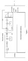
- Figure 2 represents a preferred embodiment of a satellite-based data transmission/reception device.
- Figure 2 represents a functional diagram which more particularly details the reception facility.
- the transmission facility is not detailed since any type of transmission facility can be used.
- An antenna 10 is connected to a low noise block 20, better known by the abbreviation LNB.
- the antenna 10 consists for example of a wave concentration device, such as a reflector or a lens, and of a wave to electrical signal conversion device.
- the waves received generally have frequencies for example greater than 10 GHz.
- a duplexer can be added between the antenna 10 and the LNB 20 if the transmission/reception device operates in full duplex mode.
- the LNB 20 comprises at least one first stage of low-noise amplification 21, for example of VLNA type, of one or more other low-noise amplifiers 22, of means 23 for transposing the signal received into a band of intermediate frequencies, lying for example between 500 MHz and 2 GHz, and one or more filters 24. All these elements 21 to 24 are placed according to one of the techniques known to the person skilled in the art, for example as indicated in Figure 2.
- the first amplification stage 21 is furnished with means which make it possible to neutralize the signal received.
- the means of neutralization are relatively easily implemented supply switching means.
- the output of the LNB 20 is linked to a tuner 30, for example by way of a coaxial cable if the tuner is situated in an internal unit.
- the tuner 30 comprises a variable-gain device 31, a mixer 32, a local oscillator 33, and possibly other means 34 of amplification and of filtering, these elements are for example connected as is indicated in Figure 2.
- the variable-gain device 31 is preferably an amplifier but may also be an attenuator.
- the local oscillator 33 can be a controlled oscillator which makes it possible to select a channel in the intermediate frequency band.
- the transposition carried out by the mixer 32 and the oscillator 33 transposes for example a selected channel to baseband.
- the output of the tuner 30 is connected to a device for digitizing the signal 40 which comprises sampling means and means of analogue/digital conversion which transforms the signal output by the tuner 30 into a digital signal coded on n bits.
- the digital signal is delivered to a digital processing device 50.
- the digital processing device 50 comprises a demodulation and decoding circuit 51 which on a first output delivers a stream of demodulated and decoded data to a user device (not represented).
- the demodulation and decoding circuit furthermore comprises means for recoding and remodulating the data so as to deliver on a second output a modulated signal which corresponds to the signal received without noise.
- a first power estimation circuit 52 measures the power of the digital signal.
- a second power estimation circuit 53 measures the power of the modulated signal.
- a supervisory circuit 55 delivers an on/off binary command which controls the supply to the first amplification stage 21.
- the on/off binary command can be transmitted for example with the aid of a carrier of a frequency distant from the intermediate band with the aid of the coaxial cable.
- the supervisory circuit 55 furthermore delivers commands (not represented) to the other elements of the circuit and caters for the sequencing of the digital processing device 50.
- a gain correction circuit 54 receives the power measurements originating from the two power estimation circuits 52 and 53 as well as the on/off binary signal and delivers a gain set-point to the variable-gain device.
- the on/off binary signal indicates the conditions under which the gain set-point must be formulated.
- a first automatic gain control is performed when the on/off binary signal neutralizes the first amplification stage 21.
- the neutralization can be carried out upon switching on the system and also between the reception of bursts.
- the first power estimation circuit 52 delivers the noise power of the complete transmission facility, apart from the first amplification stage 21.
- the gain correction circuit 54 will vary the gain of the variable-gain device 54 so that the power of the noise exiting the reception facility is restored to a first predetermined level.
- the predetermined level is chosen so that:
- a second automatic gain control is performed dynamically during the reception of data.
- the digital signal contains on the one hand the signal received and on the other hand noise.
- noise power several techniques are possible.
- One technique consists in measuring on the one hand the power of the digital signal and on the other hand the power of the modulated signal which corresponds to the same signal minus noise. Then on the basis of these two powers, the gain control circuit 54 calculates the power of the noise.
- the gain correction circuit 54 supervises the variable-gain device 31 so that the noise power remains at a second predetermined level.
- the second predetermined noise level is not the same as the first predetermined noise level since the latter takes into account the noise of the first amplification stage 21.
- a simple technique for obtaining the second predetermined level consists in performing the first automatic gain control then when the first stage 21 is reactivated and when a signal is locked on to (in general in a few milliseconds), the measured noise is stored as second predetermined level, thus taking account of the noise of the first stage 21 during switch-on.
- the second automatic gain control makes it possible to generate a complementary command so as to compensate for the slow drifting of the gain which is due among other things to temperature variations.
- the variation in the noise power at the input of the analogue/digital conversion means may reach 7 dB (extreme cases of contributions from noise restored at the output of a VLNA). 5 dB are due to the variation in the noise contribution observed at the output of the antenna and 2 dB to the uncertainty in the gain of the VLNA (component scatter and temperature drift).
- This uncertainty range of 7 dB in the least favourable case constitutes a marked improvement as compared with the 20 dB previously considered for an entire reception facility constructed according to the state of the art.
- the impact on the dimensioning of an analogue/digital converter is substantially smaller (1 extra bit instead of 3 bits).
- the preferred embodiment includes a first and a second gain control step, the first being “static” and the second being “dynamic".
- the combination of the two makes it possible to have continuous control of the gain of the reception facility.
- the first gain control between two bursts destined for the relevant receiver, this first control possibly being performed for example every second. In this case, the second control is not necessary.
- the neutralization of the first stage 21 is carried out by cutting off the supply.
- This simple and effective solution can be replaced by other neutralization devices.
- the supply alone can be cut off with the aid of inexpensive means. It is also possible not to neutralize the first stage, the important thing being to neutralize the signal received from the antenna as far upstream as possible in the reception facility, so as to minimize the uncertainty regarding the amplified noise level after reactivation of the complete reception facility.
- the reception facility can be modified to a large extent without departing from the scope of the invention. It is possible to use all types of reception facility.
- the LNB 20 can be replaced with a more or less complex external unit which can for example include a tuner.
- the variable-gain device 31 can be shifted over the entire length of the reception facility between the point of neutralization of the signal received and the end of the reception facility.
Landscapes
- Engineering & Computer Science (AREA)
- Signal Processing (AREA)
- Multimedia (AREA)
- Theoretical Computer Science (AREA)
- Astronomy & Astrophysics (AREA)
- General Physics & Mathematics (AREA)
- Physics & Mathematics (AREA)
- Computer Networks & Wireless Communication (AREA)
- Circuits Of Receivers In General (AREA)
- Input Circuits Of Receivers And Coupling Of Receivers And Audio Equipment (AREA)
- Control Of Amplification And Gain Control (AREA)
- Radio Relay Systems (AREA)
- Reduction Or Emphasis Of Bandwidth Of Signals (AREA)
- Radar Systems Or Details Thereof (AREA)
Abstract
Description
- The invention relates to a device with automatic gain control. Such a device is used in the facility for receiving radiofrequency communications, in particular of satellite type.
- In a conventional satellite-based communication system, the reception input stage is built around a low-noise amplifier, for example of VLNA type (standing for Very Low Noise Amplifier). A conventional receiver structure associating an antenna with a transmission/reception device is given hereinbelow. In the reception path, the first stage, the so-called VLNA stage, amplifies the useful signal output by the antenna while minimizing its contribution in terms of noise. On reception, one of the major problems to be solved is the automatic gain control (hereinafter AGC) which makes it possible to accurately adjust the gain of the reception facility, so that the amplitude of the input signal to an analog to digital converter (hereinbelow ADC) is optimal. The number of useful quantization bits is then minimized, thereby enabling or aiding construction. The critical manner of operation of such a gain control device is accentuated in the case where the signals received exhibit a wide dynamic swing of instantaneous power variation: such is the case for example for a CDMA signal (standing for Code Division Multiple Access) combining a high number of codes, for which the ratio of peak power to mean power may be high. Specifically, the minimum number of quantization bits required will then be higher than for signals exhibiting a lower ratio of peak power to mean power. The limit of operation of the device is also accentuated in the case where the power of the signal received at the level of the antenna is prone to very fast alterations over time within a wide dynamic range: such is the case for example for a CDMA signal transmitted in bursts, and for which the number of codes used and the power assigned to each of them are prone to alter from one burst to another in an unpredictable manner.
- For conventional reception of continuous-train signals (typically digital TV reception via geostationary satellite), a technique commonly implemented for solving the problem posed consists in inserting a variable-gain amplifier into the reception facility. In this case, gain control can be implemented by slaving the signal power at the input of the ADC which alters very slowly over time. Automatic gain control is then undertaken after continuous evaluation of the power, of the amplitude distribution or of the probability of peak-clipping at the output of the ADC. A variable-gain element (attenuator or amplifier) set up in the reception facility is then acted on in such a way that the amplitude of the sampled signal is optimal. The device then compensates for the variations in stream received at the level of the antenna, as well as the scatter and fluctuations in gain in the reception facility. Figure 1 describes in a simple manner the device then implemented in the reception facility.
- In the case of the reception of signals whose power may alter very rapidly and unpredictably as a function of time, the technique described above cannot be implemented. One means of allowing the demodulation of the signal then consists in taking into account the total dynamic swing of possible power variation - without any automatic control - when dimensioning the ADC. However this approach leads to a considerable oversizing of the number of quantization bits required. Specifically, the scatter in gain in a reception facility with high gain operating within a wide temperature span is very considerable (typically greater than 30 dB for 90 dB of gain and 100°C of temperature variation). This scatter can be reduced by calibrating the receiver in the factory at fixed frequency and at constant temperature but will nevertheless remain greater than 20 dB. This contribution requires the use of more than 3 extra quantization bits. These considerations may lead to a technological impossibility of construction in the case where the sampling frequency of the ADCs is high.
- The invention aims to minimize the oversizing of the ADC within the framework of the reception of signals exhibiting power levels which vary over time. The invention proposes an automatic gain control technique which handles the setting of the noise level associated with the amplified signal.
- The invention is a method of automatic gain control in a radiofrequency signal reception device, the said device comprising at least one first low-noise amplification stage placed following a reception antenna, and at least one variable-gain device placed in the reception facility. The method carries out steps of neutralization of the signal received by the antenna, and of adjustment of the gain during the neutralization of the signal received until a predetermined noise level is obtained at the end of the reception facility.
- Such a method of gain control can be carried out upon switching on the device and also between the reception of bursts.
- Preferably, one seeks to reduce the cost of construction. Accordingly, the neutralization of the signal received is carried out by cutting off the supply to the first low-noise amplification stage.
- Under certain conditions of use, it is not possible to perform control of the gain between bursts. Accordingly, a second control can be performed during the reception of the signal by performing steps of extraction of the noise power at the end of the reception facility, and of adjustment of the gain until a predetermined noise level is obtained.
- According to a second aspect, the invention is a radiofrequency signal reception device which comprises the means necessary for the implementation of the method.
- According to a third aspect, the invention is a device for transmitting/receiving radiofrequency signals transmitted by satellite which comprises the above reception device.
- The invention will be better understood and other features and advantages will become apparent on reading the description which follows, the description making reference to the appended drawings among which:
- Figure 1 represents an exemplary satellite terminal reception facility for continuous-train signals, such as is known from the state of the art,
- Figure 2 represents a satellite terminal reception facility according to the invention.
-
- Figure 2 represents a preferred embodiment of a satellite-based data transmission/reception device. Figure 2 represents a functional diagram which more particularly details the reception facility. The transmission facility is not detailed since any type of transmission facility can be used.
- An
antenna 10 is connected to a low noise block 20, better known by the abbreviation LNB. Theantenna 10 consists for example of a wave concentration device, such as a reflector or a lens, and of a wave to electrical signal conversion device. The waves received generally have frequencies for example greater than 10 GHz. A duplexer can be added between theantenna 10 and the LNB 20 if the transmission/reception device operates in full duplex mode. - The LNB 20 comprises at least one first stage of low-
noise amplification 21, for example of VLNA type, of one or more other low-noise amplifiers 22, ofmeans 23 for transposing the signal received into a band of intermediate frequencies, lying for example between 500 MHz and 2 GHz, and one ormore filters 24. All theseelements 21 to 24 are placed according to one of the techniques known to the person skilled in the art, for example as indicated in Figure 2. However, thefirst amplification stage 21 is furnished with means which make it possible to neutralize the signal received. Preferably, the means of neutralization are relatively easily implemented supply switching means. When thefirst amplification stage 21 is not supplied, the remainder of the reception facility now transmits only the noise related to the various elements making up the said facility. - The output of the LNB 20 is linked to a
tuner 30, for example by way of a coaxial cable if the tuner is situated in an internal unit. Thetuner 30 comprises a variable-gain device 31, amixer 32, alocal oscillator 33, and possibly other means 34 of amplification and of filtering, these elements are for example connected as is indicated in Figure 2. The variable-gain device 31 is preferably an amplifier but may also be an attenuator. Thelocal oscillator 33 can be a controlled oscillator which makes it possible to select a channel in the intermediate frequency band. The transposition carried out by themixer 32 and theoscillator 33 transposes for example a selected channel to baseband. - The output of the
tuner 30 is connected to a device for digitizing thesignal 40 which comprises sampling means and means of analogue/digital conversion which transforms the signal output by thetuner 30 into a digital signal coded on n bits. The digital signal is delivered to adigital processing device 50. - The
digital processing device 50 comprises a demodulation anddecoding circuit 51 which on a first output delivers a stream of demodulated and decoded data to a user device (not represented). The demodulation and decoding circuit furthermore comprises means for recoding and remodulating the data so as to deliver on a second output a modulated signal which corresponds to the signal received without noise. - A first power estimation circuit 52 measures the power of the digital signal.
- A second power estimation circuit 53 measures the power of the modulated signal.
- A
supervisory circuit 55 delivers an on/off binary command which controls the supply to thefirst amplification stage 21. The on/off binary command can be transmitted for example with the aid of a carrier of a frequency distant from the intermediate band with the aid of the coaxial cable. Thesupervisory circuit 55 furthermore delivers commands (not represented) to the other elements of the circuit and caters for the sequencing of thedigital processing device 50. - A gain correction circuit 54 receives the power measurements originating from the two power estimation circuits 52 and 53 as well as the on/off binary signal and delivers a gain set-point to the variable-gain device. The on/off binary signal indicates the conditions under which the gain set-point must be formulated.
- A first automatic gain control is performed when the on/off binary signal neutralizes the
first amplification stage 21. The neutralization can be carried out upon switching on the system and also between the reception of bursts. The first power estimation circuit 52 delivers the noise power of the complete transmission facility, apart from thefirst amplification stage 21. The gain correction circuit 54 will vary the gain of the variable-gain device 54 so that the power of the noise exiting the reception facility is restored to a first predetermined level. The predetermined level is chosen so that: - when the
first amplification stage 21 is reactivated, the noise restored at the input of the analogue/digital conversion means must be weakly affected by the quantization noise, - the peak-clipping of the useful signal combined with the noise restored by the analogue/digital conversion means must be minimized.
- A second automatic gain control is performed dynamically during the reception of data. When the
first amplification stage 21 is activated, the digital signal contains on the one hand the signal received and on the other hand noise. To get an estimate of the noise power, several techniques are possible. One technique consists in measuring on the one hand the power of the digital signal and on the other hand the power of the modulated signal which corresponds to the same signal minus noise. Then on the basis of these two powers, the gain control circuit 54 calculates the power of the noise. The gain correction circuit 54 supervises the variable-gain device 31 so that the noise power remains at a second predetermined level. - The second predetermined noise level is not the same as the first predetermined noise level since the latter takes into account the noise of the
first amplification stage 21. A simple technique for obtaining the second predetermined level consists in performing the first automatic gain control then when thefirst stage 21 is reactivated and when a signal is locked on to (in general in a few milliseconds), the measured noise is stored as second predetermined level, thus taking account of the noise of thefirst stage 21 during switch-on. - The second automatic gain control makes it possible to generate a complementary command so as to compensate for the slow drifting of the gain which is due among other things to temperature variations.
- By way of example regarding the performance of the invention, in the case of reception from a low-orbit satellite, the variation in the noise power at the input of the analogue/digital conversion means, once the
first stage 21 has been reactivated may reach 7 dB (extreme cases of contributions from noise restored at the output of a VLNA). 5 dB are due to the variation in the noise contribution observed at the output of the antenna and 2 dB to the uncertainty in the gain of the VLNA (component scatter and temperature drift). This uncertainty range of 7 dB in the least favourable case constitutes a marked improvement as compared with the 20 dB previously considered for an entire reception facility constructed according to the state of the art. In this case, the impact on the dimensioning of an analogue/digital converter is substantially smaller (1 extra bit instead of 3 bits). - Numerous variants are possible. The preferred embodiment includes a first and a second gain control step, the first being "static" and the second being "dynamic". The combination of the two makes it possible to have continuous control of the gain of the reception facility. However, in certain cases of use, it is not necessary to have continuous control. By way of example, in a system for transmitting data dedicated to a receiver and in which the transmission is carried out with the aid of a succession of bursts destined for various receivers, it is then possible to perform the first gain control between two bursts destined for the relevant receiver, this first control possibly being performed for example every second. In this case, the second control is not necessary.
- In the preferred embodiment, the neutralization of the
first stage 21 is carried out by cutting off the supply. This simple and effective solution can be replaced by other neutralization devices. However, if the signal passing through thefirst stage 21 is regarded as being of very high frequency, the supply alone can be cut off with the aid of inexpensive means. It is also possible not to neutralize the first stage, the important thing being to neutralize the signal received from the antenna as far upstream as possible in the reception facility, so as to minimize the uncertainty regarding the amplified noise level after reactivation of the complete reception facility. - The reception facility can be modified to a large extent without departing from the scope of the invention. It is possible to use all types of reception facility. The LNB 20 can be replaced with a more or less complex external unit which can for example include a tuner. The variable-gain device 31 can be shifted over the entire length of the reception facility between the point of neutralization of the signal received and the end of the reception facility.
Claims (9)
- Method of automatic control of the gain in a radiofrequency signal reception device, the said device comprising at least one first low-noise amplification stage placed following a reception antenna, and at least one variable-gain device placed in the reception facility, characterized in that the following steps are performed:neutralization of the signal received by the antenna,adjustment of the gain during the neutralization of the signal received until a predetermined noise level is obtained at the end of the reception facility.
- Method according to Claim 1, characterized in that the neutralization of the signal received is carried out by cutting off the supply to the first low-noise amplification stage.
- Method according to one of Claims 1 or 2, characterized in that, during signal reception, the following steps are performed:extraction of the noise power at the end of the reception facility,adjustment of the gain until a predetermined noise level is obtained.
- Method according to Claim 3, characterized in that the extraction of the noise power at the end of the facility is carried out by performing the following steps:sampling and digitization of the signal at the end of the reception facility,digital demodulation of the digitized signal,modulation of the demodulated signal,calculation of the noise power from the modulated signal and the digitized signal.
- Radiofrequency signal reception device, the said device comprising at least one first low-noise amplification stage placed following a reception antenna, and at least one variable-gain device placed in the reception facility, characterized in that it comprises:means for neutralizing the signal received by the antenna,means for adjusting the variable-gain device as a function of the noise level at the end of the reception facility.
- Device according to Claim 5, characterized in that the means for neutralizing the signal received are switching means which switch the supply of the first amplification stage.
- Device according to one of Claims 5 or 6, characterized in that it furthermore comprises:means for extracting the noise power during the reception of the signal,means for adjusting the variable-gain device as a function of the noise level extracted.
- Device according to Claim 7, characterized in that the means for extracting the noise power during reception comprise :means of sampling and means of converting the signal at the end of the facility into a digitized signal,means for performing the digital demodulation of the signal and for obtaining a demodulated signal,means of digital modulation for modulating the demodulated signal and obtaining a modulated signal,means for calculating the noise power from the modulated signal and the digitized signal.
- Device for transmitting/receiving radiofrequency signals transmitted by satellite, characterized in that it comprises the reception device of one of Claims 5 to 8.
Applications Claiming Priority (2)
| Application Number | Priority Date | Filing Date | Title |
|---|---|---|---|
| FR0102202 | 2001-02-16 | ||
| FR0102202A FR2821228B1 (en) | 2001-02-16 | 2001-02-16 | AUTOMATIC GAIN CONTROL RECEIVING DEVICE |
Publications (2)
| Publication Number | Publication Date |
|---|---|
| EP1233615A1 true EP1233615A1 (en) | 2002-08-21 |
| EP1233615B1 EP1233615B1 (en) | 2011-01-26 |
Family
ID=8860163
Family Applications (1)
| Application Number | Title | Priority Date | Filing Date |
|---|---|---|---|
| EP02002536A Expired - Lifetime EP1233615B1 (en) | 2001-02-16 | 2002-02-04 | Receiving device with automatic gain control |
Country Status (9)
| Country | Link |
|---|---|
| US (1) | US7046976B2 (en) |
| EP (1) | EP1233615B1 (en) |
| JP (1) | JP2002280854A (en) |
| KR (1) | KR20020067636A (en) |
| CN (1) | CN1371214A (en) |
| AT (1) | ATE497319T1 (en) |
| DE (1) | DE60239026D1 (en) |
| FR (1) | FR2821228B1 (en) |
| MX (1) | MXPA02001541A (en) |
Cited By (2)
| Publication number | Priority date | Publication date | Assignee | Title |
|---|---|---|---|---|
| EP1923993A1 (en) * | 2006-11-08 | 2008-05-21 | Dibcom | Method and device for digitizing an analogical signal |
| US7944383B2 (en) | 2006-12-14 | 2011-05-17 | Nxp B.V. | Data processing device comprising ADC unit |
Families Citing this family (17)
| Publication number | Priority date | Publication date | Assignee | Title |
|---|---|---|---|---|
| JP2003218711A (en) * | 2002-01-22 | 2003-07-31 | Alps Electric Co Ltd | Agc circuit of fm receiver |
| CA2518476A1 (en) * | 2003-03-14 | 2004-09-30 | Interdigital Technology Corporation | Enhanced automatic gain control mechanism for timeslotted data transmissions |
| KR100480646B1 (en) * | 2003-04-17 | 2005-03-31 | 삼성전자주식회사 | Automatic gain controller providing for stable signal acquisition and tracking adaptive in high-noise multipath channels, digital television receiver comprising it and method thereof |
| CN100373812C (en) * | 2003-06-05 | 2008-03-05 | 中兴通讯股份有限公司 | Calibration device and method for array receiver automatic gain control circuit |
| US7773702B2 (en) * | 2004-05-03 | 2010-08-10 | Qualcomm Incorporated | Gain control for a receiver in a multi-carrier communication system |
| US7693491B2 (en) * | 2004-11-30 | 2010-04-06 | Broadcom Corporation | Method and system for transmitter output power compensation |
| KR100680252B1 (en) | 2005-04-08 | 2007-02-07 | 엔지엘테크놀러지 주식회사 | Connection device of mobile communication system |
| KR100983547B1 (en) * | 2005-11-21 | 2010-09-24 | 후지쓰 텐 가부시키가이샤 | Receiver apparatus |
| US20070117515A1 (en) * | 2005-11-23 | 2007-05-24 | Sr Technologies, Inc. | Burst processor method and apparatus |
| CN100525123C (en) * | 2006-08-10 | 2009-08-05 | 华为技术有限公司 | Receiver and wireless signal receiving method |
| JP2008053895A (en) * | 2006-08-23 | 2008-03-06 | Fujitsu Ltd | Radio receiver and gain control method thereof |
| JP2010515292A (en) * | 2006-12-25 | 2010-05-06 | トムソン ライセンシング | Method and apparatus for automatic gain control |
| US8401507B2 (en) * | 2007-12-21 | 2013-03-19 | Motorola Mobility Llc | Automatic gain control for beamformed signals |
| JP7056889B2 (en) * | 2017-01-20 | 2022-04-19 | ソニーセミコンダクタソリューションズ株式会社 | Antenna device and receiver |
| KR20190101400A (en) * | 2017-01-20 | 2019-08-30 | 소니 세미컨덕터 솔루션즈 가부시키가이샤 | Antenna device and receiver |
| CN110290578B (en) | 2018-03-19 | 2021-09-03 | 大唐移动通信设备有限公司 | Method and terminal for acquiring noise power |
| US11804811B2 (en) * | 2021-04-29 | 2023-10-31 | Silicon Laboratories Inc. | Apparatus for determining when an automatic gain control circuit has settled |
Citations (2)
| Publication number | Priority date | Publication date | Assignee | Title |
|---|---|---|---|---|
| JPS56108947A (en) | 1980-02-01 | 1981-08-28 | Mitsubishi Electric Corp | Radio receiver for microwave radiometer |
| EP0777335A2 (en) * | 1995-12-04 | 1997-06-04 | Sharp Kabushiki Kaisha | Satellite broadcast tuner capable of processing both QPSK modulation signal and FM signal |
Family Cites Families (13)
| Publication number | Priority date | Publication date | Assignee | Title |
|---|---|---|---|---|
| JPS6027234A (en) * | 1983-07-22 | 1985-02-12 | Nec Corp | Receiver |
| US5199045A (en) * | 1987-06-09 | 1993-03-30 | Canon Kabushiki Kaisha | Communication apparatus |
| KR950701472A (en) * | 1992-06-08 | 1995-03-23 | 다니엘 케이. 니콜스 | Receiver automatic gain control |
| JPH09270723A (en) * | 1996-03-29 | 1997-10-14 | Alps Electric Co Ltd | Ic for reception circuit for portable telephone set |
| JPH1065568A (en) * | 1996-08-21 | 1998-03-06 | Oki Electric Ind Co Ltd | Radio equipment |
| JPH11136154A (en) * | 1997-10-31 | 1999-05-21 | Sony Corp | Receiver |
| US6134430A (en) * | 1997-12-09 | 2000-10-17 | Younis; Saed G. | Programmable dynamic range receiver with adjustable dynamic range analog to digital converter |
| US6324387B1 (en) * | 1998-12-29 | 2001-11-27 | Philips Electronics N.A. Corp. | LNA control-circuit for receive closed loop automatic gain control |
| EP1083668A4 (en) * | 1999-02-25 | 2004-06-16 | Mitsubishi Electric Corp | RADIO STATION UNIT |
| US6690944B1 (en) * | 1999-04-12 | 2004-02-10 | Nortel Networks Limited | Power control of a multi-subchannel mobile station in a mobile communication system |
| US6285863B1 (en) * | 1999-11-24 | 2001-09-04 | Lucent Technologies Inc. | System and method for providing automatic gain control with high dynamic range |
| US6288609B1 (en) * | 2000-02-29 | 2001-09-11 | Motorola, Inc. | Gain controllable low noise amplifier with automatic linearity enhancement and method of doing same |
| US6804501B1 (en) * | 2000-09-25 | 2004-10-12 | Prairiecomm, Inc. | Receiver having gain control and narrowband interference detection |
-
2001
- 2001-02-16 FR FR0102202A patent/FR2821228B1/en not_active Expired - Fee Related
-
2002
- 2002-02-04 DE DE60239026T patent/DE60239026D1/en not_active Expired - Lifetime
- 2002-02-04 AT AT02002536T patent/ATE497319T1/en not_active IP Right Cessation
- 2002-02-04 EP EP02002536A patent/EP1233615B1/en not_active Expired - Lifetime
- 2002-02-08 KR KR1020020007513A patent/KR20020067636A/en not_active Ceased
- 2002-02-11 CN CN02105036A patent/CN1371214A/en active Pending
- 2002-02-13 MX MXPA02001541A patent/MXPA02001541A/en not_active Application Discontinuation
- 2002-02-13 US US10/075,833 patent/US7046976B2/en not_active Expired - Lifetime
- 2002-02-15 JP JP2002038950A patent/JP2002280854A/en active Pending
Patent Citations (2)
| Publication number | Priority date | Publication date | Assignee | Title |
|---|---|---|---|---|
| JPS56108947A (en) | 1980-02-01 | 1981-08-28 | Mitsubishi Electric Corp | Radio receiver for microwave radiometer |
| EP0777335A2 (en) * | 1995-12-04 | 1997-06-04 | Sharp Kabushiki Kaisha | Satellite broadcast tuner capable of processing both QPSK modulation signal and FM signal |
Non-Patent Citations (1)
| Title |
|---|
| PATENT ABSTRACTS OF JAPAN vol. 005, no. 113 (P - 089) 13 November 1981 (1981-11-13) * |
Cited By (2)
| Publication number | Priority date | Publication date | Assignee | Title |
|---|---|---|---|---|
| EP1923993A1 (en) * | 2006-11-08 | 2008-05-21 | Dibcom | Method and device for digitizing an analogical signal |
| US7944383B2 (en) | 2006-12-14 | 2011-05-17 | Nxp B.V. | Data processing device comprising ADC unit |
Also Published As
| Publication number | Publication date |
|---|---|
| FR2821228B1 (en) | 2003-04-11 |
| ATE497319T1 (en) | 2011-02-15 |
| MXPA02001541A (en) | 2010-11-19 |
| CN1371214A (en) | 2002-09-25 |
| US7046976B2 (en) | 2006-05-16 |
| FR2821228A1 (en) | 2002-08-23 |
| KR20020067636A (en) | 2002-08-23 |
| EP1233615B1 (en) | 2011-01-26 |
| JP2002280854A (en) | 2002-09-27 |
| US20020115419A1 (en) | 2002-08-22 |
| DE60239026D1 (en) | 2011-03-10 |
Similar Documents
| Publication | Publication Date | Title |
|---|---|---|
| US7046976B2 (en) | Receiving device with automatic gain control | |
| US6806844B2 (en) | Calibration system for array antenna receiving apparatus | |
| US7483500B2 (en) | Narrowband gain control of receiver with digital post filtering | |
| US6226504B1 (en) | Receiving apparatus | |
| CN101917170B (en) | Direct conversion receiver architecture | |
| KR0133338B1 (en) | Digital automatic gain control device for satellite repeater | |
| US20020118780A1 (en) | Pro-active antenna switching based on relative power | |
| US6775336B1 (en) | Receiver and gain control method of the same | |
| WO2008066290A1 (en) | Automatic gain control circuit and method for automatic gain control | |
| US20040156097A1 (en) | Intelligent gain control in an on-frequency repeater | |
| US20030081706A1 (en) | Noise reduction filtering in a wireless communication system | |
| JP2002280854A5 (en) | ||
| KR20050006209A (en) | Digital automatic gain control for transceiver devices | |
| EP0771069B1 (en) | Apparatus for controlling the conversion gain of a down converter | |
| US8446984B2 (en) | Method and system for identification of portable antenna modules | |
| WO2005015773A1 (en) | Array antenna receiver apparatus and received signal correcting method | |
| JP2001339455A (en) | Receiving device and wireless communication device | |
| US7076203B2 (en) | Apparatus and method for receiving transmit wave | |
| KR20010050670A (en) | Method and apparatus for power based dynamic channel allocation for receiver dynamic range mitigation | |
| CN117560027A (en) | Signal receiver and signal receiving method | |
| JP2006512828A (en) | Control technique for mobile handset transmit power | |
| US20040248536A1 (en) | Receiving circuit having improved distortion characteristics | |
| KR101766813B1 (en) | Digital input overflow processing device | |
| JPH04170232A (en) | Transmission power control system | |
| JP2024056181A (en) | TRANSMISSION CIRCUIT, COMMUNICATION DEVICE, COMMUNICATION METHOD, AND PROGRAM |
Legal Events
| Date | Code | Title | Description |
|---|---|---|---|
| PUAI | Public reference made under article 153(3) epc to a published international application that has entered the european phase |
Free format text: ORIGINAL CODE: 0009012 |
|
| AK | Designated contracting states |
Kind code of ref document: A1 Designated state(s): AT BE CH CY DE DK ES FI FR GB GR IE IT LI LU MC NL PT SE TR |
|
| AX | Request for extension of the european patent |
Free format text: AL;LT;LV;MK;RO;SI |
|
| AKX | Designation fees paid | ||
| 17P | Request for examination filed |
Effective date: 20030210 |
|
| RBV | Designated contracting states (corrected) |
Designated state(s): AT BE CH CY DE DK ES FI FR GB GR IE IT LI LU MC NL PT SE TR |
|
| REG | Reference to a national code |
Ref country code: DE Ref legal event code: 8566 |
|
| RAP1 | Party data changed (applicant data changed or rights of an application transferred) |
Owner name: THOMSON LICENSING |
|
| 17Q | First examination report despatched |
Effective date: 20070209 |
|
| RAP1 | Party data changed (applicant data changed or rights of an application transferred) |
Owner name: THOMSON LICENSING |
|
| GRAP | Despatch of communication of intention to grant a patent |
Free format text: ORIGINAL CODE: EPIDOSNIGR1 |
|
| GRAS | Grant fee paid |
Free format text: ORIGINAL CODE: EPIDOSNIGR3 |
|
| GRAA | (expected) grant |
Free format text: ORIGINAL CODE: 0009210 |
|
| AK | Designated contracting states |
Kind code of ref document: B1 Designated state(s): AT BE CH CY DE DK ES FI FR GB GR IE IT LI LU MC NL PT SE TR |
|
| REG | Reference to a national code |
Ref country code: GB Ref legal event code: FG4D |
|
| REG | Reference to a national code |
Ref country code: CH Ref legal event code: EP |
|
| REG | Reference to a national code |
Ref country code: DE Ref legal event code: R084 Ref document number: 60239026 Country of ref document: DE |
|
| REG | Reference to a national code |
Ref country code: IE Ref legal event code: FG4D |
|
| REF | Corresponds to: |
Ref document number: 60239026 Country of ref document: DE Date of ref document: 20110310 Kind code of ref document: P |
|
| REG | Reference to a national code |
Ref country code: DE Ref legal event code: R096 Ref document number: 60239026 Country of ref document: DE Effective date: 20110310 |
|
| REG | Reference to a national code |
Ref country code: NL Ref legal event code: VDEP Effective date: 20110126 |
|
| PG25 | Lapsed in a contracting state [announced via postgrant information from national office to epo] |
Ref country code: ES Free format text: LAPSE BECAUSE OF FAILURE TO SUBMIT A TRANSLATION OF THE DESCRIPTION OR TO PAY THE FEE WITHIN THE PRESCRIBED TIME-LIMIT Effective date: 20110507 Ref country code: SE Free format text: LAPSE BECAUSE OF FAILURE TO SUBMIT A TRANSLATION OF THE DESCRIPTION OR TO PAY THE FEE WITHIN THE PRESCRIBED TIME-LIMIT Effective date: 20110126 Ref country code: GR Free format text: LAPSE BECAUSE OF FAILURE TO SUBMIT A TRANSLATION OF THE DESCRIPTION OR TO PAY THE FEE WITHIN THE PRESCRIBED TIME-LIMIT Effective date: 20110427 Ref country code: PT Free format text: LAPSE BECAUSE OF FAILURE TO SUBMIT A TRANSLATION OF THE DESCRIPTION OR TO PAY THE FEE WITHIN THE PRESCRIBED TIME-LIMIT Effective date: 20110526 |
|
| PG25 | Lapsed in a contracting state [announced via postgrant information from national office to epo] |
Ref country code: AT Free format text: LAPSE BECAUSE OF FAILURE TO SUBMIT A TRANSLATION OF THE DESCRIPTION OR TO PAY THE FEE WITHIN THE PRESCRIBED TIME-LIMIT Effective date: 20110126 Ref country code: CY Free format text: LAPSE BECAUSE OF FAILURE TO SUBMIT A TRANSLATION OF THE DESCRIPTION OR TO PAY THE FEE WITHIN THE PRESCRIBED TIME-LIMIT Effective date: 20110126 Ref country code: BE Free format text: LAPSE BECAUSE OF FAILURE TO SUBMIT A TRANSLATION OF THE DESCRIPTION OR TO PAY THE FEE WITHIN THE PRESCRIBED TIME-LIMIT Effective date: 20110126 Ref country code: FI Free format text: LAPSE BECAUSE OF FAILURE TO SUBMIT A TRANSLATION OF THE DESCRIPTION OR TO PAY THE FEE WITHIN THE PRESCRIBED TIME-LIMIT Effective date: 20110126 Ref country code: NL Free format text: LAPSE BECAUSE OF FAILURE TO SUBMIT A TRANSLATION OF THE DESCRIPTION OR TO PAY THE FEE WITHIN THE PRESCRIBED TIME-LIMIT Effective date: 20110126 |
|
| PG25 | Lapsed in a contracting state [announced via postgrant information from national office to epo] |
Ref country code: MC Free format text: LAPSE BECAUSE OF NON-PAYMENT OF DUE FEES Effective date: 20110228 |
|
| REG | Reference to a national code |
Ref country code: CH Ref legal event code: PL |
|
| PG25 | Lapsed in a contracting state [announced via postgrant information from national office to epo] |
Ref country code: CH Free format text: LAPSE BECAUSE OF NON-PAYMENT OF DUE FEES Effective date: 20110228 Ref country code: DK Free format text: LAPSE BECAUSE OF FAILURE TO SUBMIT A TRANSLATION OF THE DESCRIPTION OR TO PAY THE FEE WITHIN THE PRESCRIBED TIME-LIMIT Effective date: 20110126 Ref country code: LI Free format text: LAPSE BECAUSE OF NON-PAYMENT OF DUE FEES Effective date: 20110228 |
|
| REG | Reference to a national code |
Ref country code: IE Ref legal event code: MM4A |
|
| PLBE | No opposition filed within time limit |
Free format text: ORIGINAL CODE: 0009261 |
|
| STAA | Information on the status of an ep patent application or granted ep patent |
Free format text: STATUS: NO OPPOSITION FILED WITHIN TIME LIMIT |
|
| 26N | No opposition filed |
Effective date: 20111027 |
|
| PG25 | Lapsed in a contracting state [announced via postgrant information from national office to epo] |
Ref country code: IE Free format text: LAPSE BECAUSE OF NON-PAYMENT OF DUE FEES Effective date: 20110204 |
|
| REG | Reference to a national code |
Ref country code: DE Ref legal event code: R097 Ref document number: 60239026 Country of ref document: DE Effective date: 20111027 |
|
| PG25 | Lapsed in a contracting state [announced via postgrant information from national office to epo] |
Ref country code: IT Free format text: LAPSE BECAUSE OF FAILURE TO SUBMIT A TRANSLATION OF THE DESCRIPTION OR TO PAY THE FEE WITHIN THE PRESCRIBED TIME-LIMIT Effective date: 20110126 |
|
| PG25 | Lapsed in a contracting state [announced via postgrant information from national office to epo] |
Ref country code: LU Free format text: LAPSE BECAUSE OF NON-PAYMENT OF DUE FEES Effective date: 20110204 |
|
| PG25 | Lapsed in a contracting state [announced via postgrant information from national office to epo] |
Ref country code: TR Free format text: LAPSE BECAUSE OF FAILURE TO SUBMIT A TRANSLATION OF THE DESCRIPTION OR TO PAY THE FEE WITHIN THE PRESCRIBED TIME-LIMIT Effective date: 20110126 |
|
| REG | Reference to a national code |
Ref country code: FR Ref legal event code: PLFP Year of fee payment: 15 |
|
| REG | Reference to a national code |
Ref country code: FR Ref legal event code: PLFP Year of fee payment: 16 |
|
| REG | Reference to a national code |
Ref country code: DE Ref legal event code: R082 Ref document number: 60239026 Country of ref document: DE Representative=s name: DEHNS, DE Ref country code: DE Ref legal event code: R082 Ref document number: 60239026 Country of ref document: DE Representative=s name: DEHNS PATENT AND TRADEMARK ATTORNEYS, DE Ref country code: DE Ref legal event code: R082 Ref document number: 60239026 Country of ref document: DE Representative=s name: HOFSTETTER, SCHURACK & PARTNER PATENT- UND REC, DE |
|
| REG | Reference to a national code |
Ref country code: FR Ref legal event code: PLFP Year of fee payment: 17 |
|
| REG | Reference to a national code |
Ref country code: FR Ref legal event code: TP Owner name: THOMSON LICENSING DTV, FR Effective date: 20180830 |
|
| REG | Reference to a national code |
Ref country code: GB Ref legal event code: 732E Free format text: REGISTERED BETWEEN 20180927 AND 20181005 |
|
| REG | Reference to a national code |
Ref country code: DE Ref legal event code: R082 Ref document number: 60239026 Country of ref document: DE Representative=s name: DEHNS, DE Ref country code: DE Ref legal event code: R081 Ref document number: 60239026 Country of ref document: DE Owner name: INTERDIGITAL MADISON PATENT HOLDINGS, FR Free format text: FORMER OWNER: THOMSON LICENSING, ISSY-LES-MOULINEAUX, FR Ref country code: DE Ref legal event code: R082 Ref document number: 60239026 Country of ref document: DE Representative=s name: DEHNS PATENT AND TRADEMARK ATTORNEYS, DE |
|
| PGFP | Annual fee paid to national office [announced via postgrant information from national office to epo] |
Ref country code: FR Payment date: 20210223 Year of fee payment: 20 |
|
| PGFP | Annual fee paid to national office [announced via postgrant information from national office to epo] |
Ref country code: DE Payment date: 20210225 Year of fee payment: 20 Ref country code: GB Payment date: 20210223 Year of fee payment: 20 |
|
| REG | Reference to a national code |
Ref country code: GB Ref legal event code: PE20 Expiry date: 20220203 |
|
| PG25 | Lapsed in a contracting state [announced via postgrant information from national office to epo] |
Ref country code: GB Free format text: LAPSE BECAUSE OF EXPIRATION OF PROTECTION Effective date: 20220203 |