EP1233528A1 - High-frequency composite switch module - Google Patents
High-frequency composite switch module Download PDFInfo
- Publication number
- EP1233528A1 EP1233528A1 EP01974706A EP01974706A EP1233528A1 EP 1233528 A1 EP1233528 A1 EP 1233528A1 EP 01974706 A EP01974706 A EP 01974706A EP 01974706 A EP01974706 A EP 01974706A EP 1233528 A1 EP1233528 A1 EP 1233528A1
- Authority
- EP
- European Patent Office
- Prior art keywords
- laminated body
- switch module
- saw filter
- hybrid switch
- chip
- Prior art date
- Legal status (The legal status is an assumption and is not a legal conclusion. Google has not performed a legal analysis and makes no representation as to the accuracy of the status listed.)
- Withdrawn
Links
Images






Classifications
-
- H—ELECTRICITY
- H04—ELECTRIC COMMUNICATION TECHNIQUE
- H04B—TRANSMISSION
- H04B1/00—Details of transmission systems, not covered by a single one of groups H04B3/00 - H04B13/00; Details of transmission systems not characterised by the medium used for transmission
- H04B1/38—Transceivers, i.e. devices in which transmitter and receiver form a structural unit and in which at least one part is used for functions of transmitting and receiving
- H04B1/40—Circuits
- H04B1/50—Circuits using different frequencies for the two directions of communication
-
- H—ELECTRICITY
- H04—ELECTRIC COMMUNICATION TECHNIQUE
- H04B—TRANSMISSION
- H04B1/00—Details of transmission systems, not covered by a single one of groups H04B3/00 - H04B13/00; Details of transmission systems not characterised by the medium used for transmission
- H04B1/38—Transceivers, i.e. devices in which transmitter and receiver form a structural unit and in which at least one part is used for functions of transmitting and receiving
- H04B1/40—Circuits
- H04B1/44—Transmit/receive switching
- H04B1/48—Transmit/receive switching in circuits for connecting transmitter and receiver to a common transmission path, e.g. by energy of transmitter
-
- H—ELECTRICITY
- H04—ELECTRIC COMMUNICATION TECHNIQUE
- H04B—TRANSMISSION
- H04B1/00—Details of transmission systems, not covered by a single one of groups H04B3/00 - H04B13/00; Details of transmission systems not characterised by the medium used for transmission
- H04B1/38—Transceivers, i.e. devices in which transmitter and receiver form a structural unit and in which at least one part is used for functions of transmitting and receiving
- H04B1/40—Circuits
- H04B1/403—Circuits using the same oscillator for generating both the transmitter frequency and the receiver local oscillator frequency
- H04B1/406—Circuits using the same oscillator for generating both the transmitter frequency and the receiver local oscillator frequency with more than one transmission mode, e.g. analog and digital modes
-
- H—ELECTRICITY
- H10—SEMICONDUCTOR DEVICES; ELECTRIC SOLID-STATE DEVICES NOT OTHERWISE PROVIDED FOR
- H10W—GENERIC PACKAGES, INTERCONNECTIONS, CONNECTORS OR OTHER CONSTRUCTIONAL DETAILS OF DEVICES COVERED BY CLASS H10
- H10W72/00—Interconnections or connectors in packages
- H10W72/50—Bond wires
- H10W72/541—Dispositions of bond wires
- H10W72/5449—Dispositions of bond wires not being orthogonal to a side surface of the chip, e.g. fan-out arrangements
-
- H—ELECTRICITY
- H10—SEMICONDUCTOR DEVICES; ELECTRIC SOLID-STATE DEVICES NOT OTHERWISE PROVIDED FOR
- H10W—GENERIC PACKAGES, INTERCONNECTIONS, CONNECTORS OR OTHER CONSTRUCTIONAL DETAILS OF DEVICES COVERED BY CLASS H10
- H10W74/00—Encapsulations, e.g. protective coatings
- H10W74/10—Encapsulations, e.g. protective coatings characterised by their shape or disposition
- H10W74/15—Encapsulations, e.g. protective coatings characterised by their shape or disposition on active surfaces of flip-chip devices, e.g. underfills
-
- H—ELECTRICITY
- H10—SEMICONDUCTOR DEVICES; ELECTRIC SOLID-STATE DEVICES NOT OTHERWISE PROVIDED FOR
- H10W—GENERIC PACKAGES, INTERCONNECTIONS, CONNECTORS OR OTHER CONSTRUCTIONAL DETAILS OF DEVICES COVERED BY CLASS H10
- H10W90/00—Package configurations
- H10W90/701—Package configurations characterised by the relative positions of pads or connectors relative to package parts
- H10W90/721—Package configurations characterised by the relative positions of pads or connectors relative to package parts of bump connectors
- H10W90/724—Package configurations characterised by the relative positions of pads or connectors relative to package parts of bump connectors between a chip and a stacked insulating package substrate, interposer or RDL
-
- H—ELECTRICITY
- H10—SEMICONDUCTOR DEVICES; ELECTRIC SOLID-STATE DEVICES NOT OTHERWISE PROVIDED FOR
- H10W—GENERIC PACKAGES, INTERCONNECTIONS, CONNECTORS OR OTHER CONSTRUCTIONAL DETAILS OF DEVICES COVERED BY CLASS H10
- H10W90/00—Package configurations
- H10W90/701—Package configurations characterised by the relative positions of pads or connectors relative to package parts
- H10W90/731—Package configurations characterised by the relative positions of pads or connectors relative to package parts of die-attach connectors
- H10W90/734—Package configurations characterised by the relative positions of pads or connectors relative to package parts of die-attach connectors between a chip and a stacked insulating package substrate, interposer or RDL
-
- H—ELECTRICITY
- H10—SEMICONDUCTOR DEVICES; ELECTRIC SOLID-STATE DEVICES NOT OTHERWISE PROVIDED FOR
- H10W—GENERIC PACKAGES, INTERCONNECTIONS, CONNECTORS OR OTHER CONSTRUCTIONAL DETAILS OF DEVICES COVERED BY CLASS H10
- H10W90/00—Package configurations
- H10W90/701—Package configurations characterised by the relative positions of pads or connectors relative to package parts
- H10W90/751—Package configurations characterised by the relative positions of pads or connectors relative to package parts of bond wires
- H10W90/754—Package configurations characterised by the relative positions of pads or connectors relative to package parts of bond wires between a chip and a stacked insulating package substrate, interposer or RDL
Definitions
- the present invention relates to a radio-frequency hybrid switch module for use in mobile communications equipment including a mobile phone.
- Fig. 1 is a circuit block diagram of an antenna duplexer used in a GSMIDCS dual-band mobile phone conforming to European standards for mobile communications based on a Time Division Multiple Access system.
- the antenna duplexer includes antenna terminal 1, GSM-band transmitting (GSM-TX) terminal 2, GSM-band receiving (GSM-RX) terminal 3, DCS-band transmitting (DCS-TX) terminal 4, DCS-band receiving (DCS-RX) terminal 5, diplexer 6 for separating and combining frequency components in GSM and DCS bands, switches 7, 8 for switching between transmission and reception, low pass filters (LPFs) 9, 11 for removing unwanted harmonic signals, and surface acoustic wave (SAW) filters 10, 12 for allowing a band of received frequencies to pass.
- GSM-TX GSM-band transmitting
- GSM-RX DCS-band transmitting
- DCS-RX DCS-band receiving
- Fig. 10 shows a structure of a conventional antenna duplexer.
- This antenna duplexer includes ceramic multi-layer substrate 18, alumina package 19, SAW device chip 20, bonding wire 21, lid 22 of alumina package 19, diodes 23 functioning as switching devices, chip devices 24, pad 25 formed on the alumina package for wire bonding, and metal cap 26.
- Ceramic multi-layer substrate 18 includes a LPF and a diplexer formed therein.
- SAW chip 20 is put in alumina package 19 and mounted over ceramic multi-layer substrate 18.
- a small radio-frequency (RF) hybrid switch module is provided for switching between transmit-signals and receive-signals in plural frequency bands.
- This module includes: a laminated body having a dielectric layer; a diplexer; a switching circuit; a low pass filter (LPF); a conductive pattern on the dielectric layer for forming at least one of the diplexer, the switching circuit and the LPF; a surface acoustic wave (SAW) filter mounted on the laminated body; a cover on the SAW filter for forming a cavity which allows surface acoustic wave vibration and hermetically sealing the cavity; and a semiconductor switching device mounted on the laminated body for forming a part of the switching circuit.
- a laminated body having a dielectric layer; a diplexer; a switching circuit; a low pass filter (LPF); a conductive pattern on the dielectric layer for forming at least one of the diplexer, the switching circuit and the LPF; a surface acoustic wave (SAW) filter mounted on the laminated body; a cover on the SAW filter for forming a cavity which allows surface acoustic wave vibration and hermet
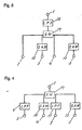
- Figs. 1-4 are circuit block diagrams each illustrating a radio-frequency (RF) hybrid switch module for a GSM/DCS mobile phone conforming with European standards for mobile communications.
- the module includes switch 13 for switching between transmission and reception in GSM and DCS bands, diplexers 14, 15, low pass filters (LPFs) 9, 11 for removing harmonics, and SP4T switch 17.
- LPFs low pass filters
- antenna terminal 1 is connected to diplexer 6 which separates and combines signals in the GSM and DCS bands.
- Respective terminals for the GSM and DCS bands of diplexer 6 are connected to switches 7 and 8, respectively.
- Transmitting sides of switches 7, 8 are connected to LPFs 9, 11, respectively, while receiving sides of switches 7, 8 are connected to surface acoustic wave (SAW) filters 10, 12, respectively.
- Filters 9,10,11,12 are connected to terminals 2, 3, 4 and 5, respectively.
- an antenna terminal is connected to switch 13.
- Switch 13 separates signals into transmitted signals and received signals.
- Diplexers 14, 15 separate and combine the signals in the GSM and DCS bands.
- Transmitting terminals of diplexer 14 are connected to LPFs 9 and 11, respectively, while receiving terminals of diplexer 15 are connected to SAW filters 10 and 12, respectively.
- Filters 9, 10, 11, 12 are connected to terminals 2, 3, 4 and 5, respectively.
- LPF 16 for removing a harmonic component from a transmitted signal is connected to antenna terminal 1.
- SP4T switch 17 allocates the transmitted signals and received signals among terminals 2, 3, 4, and 5. Receiving terminals of switch 17 are coupled to terminals 3, 5 via SAW filters 10, 12, respectively.
- SP4T switch 17 is connected to antenna terminal 1. Transmitting terminals of switch 17 are connected to LPFs 9, 11, respectively, while receiving terminals of switch 17 are connected to SAW filters 10, 12, respectively. Filters 9, 11, 10, 12 are connected to terminals 2, 3, 4 and 5, respectively.
- switches 7, 8, 13, 17 are each formed of a semiconductor switching device; e.g. a diode or a field effect transistor.
- LPFs 9, 11, 16 and diplexers 6, 14, 15 are formed of a conductive pattern provided on a dielectric layer. This dielectric layer and other dielectric layer form a laminated body.
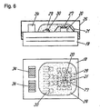
- Fig. 5 shows an RF hybrid switch module in accordance with the first embodiment.
- the module includes cover (hereinafter referred to as "micro-cavity") 27 defining a cavity at an elastic vibrating portion of SAW filter chip 20, potting resin 28, and pad 29 formed on laminated body 18 for wire bonding.
- cover hereinafter referred to as "micro-cavity”
- the elastic surface portion of SAW filter chip 20 is formed with micro-cavity 27and fortified with potting resin 28, thereby being hermetically sealed over laminated body 18 without interfering an elastic vibration.
- Chip devices 23, 24 are mounted next to chip 20.
- the module of this embodiment has a smaller size and a lower profile than a conventional module and can be manufactured inexpensively since this module does not require an alumina package.
- the plate-like laminated body 18 may be divided into an area for SAW filter chip 20 and an area for chip devices 23, 24, thus allowing only the area for the chip devices, for example, to have soldering paste printed thereon, to be subjected to reflow, and to be cleaned. This facilitates the chip devices to be mounted easily and enhances cost reduction of the module.
- Fig. 6 shows a radio-frequency hybrid switch module in accordance with a second exemplary embodiment of the present invention.
- An elastic surface portion of SAW filter chip 20 is provided with micro-cavity 27, a cover defining a cavity.
- Micro-cavity 27 is fortified with potting resin 28 as in the module shown in Fig. 5, thus allowing the elastic surface portion to be hermetically sealed over laminated body 18 without interfering with elastic vibration.
- Bare-chip diode 30 is mounted on laminated body 18 similarly to SAW filter chip 20 and coated with potting resin 28.
- the module of the present embodiment has a smaller size and a lower profile than a conventional module and can be manufactured inexpensively since this module does not require an alumina package.
- plate-like laminated body 18 is divided into an area for SAW filter chip 20 and an area for chip devices 23, 24 thus allowing only the area for the chip devices, for example, to have soldering paste printed thereon, to be subjected to reflow, and to be cleaned. This facilitates the chip devices to be mounted easily and enhances cost reduction of the module.
- the similar advantages are obtainable even if a semiconductor switching device, e.g. a field effect transistor, is used instead of bare-chip diode 30.
- wall 33 made of resin may be provided on the periphery of the bare chips on the laminated body.
- Wall 33 is taller than the bare chips.
- the bare chips placed across wall 33 from the chip devices may be covered with the potting resin.
- the potting resin is prevented from flowing into a region not requiring the potting resin, and a region to be covered with the potting resin is limited. Accordingly, a clearance for an overflowing potting resin can be minimized, and this reduces the size of the module easily and improves production yield of the module.
- Wall 33 may be formed next to chip devices 24 or may be formed to enclose the bare chips (including SAW filter chip 20 and bare-chip diode 30 in Fig. 6).
- At least one of the SAW filter and the bare chip is disposed on one side of the laminated body.
- the bare chips are separated from the chip devices on the laminated body by being disposed in the area positioned in horizontal or vertical relation to the area for the chip devices. This allows the module to be manufactured since soldering paste can be applied to laminated body 18 by thick film printing to solder the chip devices, and since flux can be cleaned efficiently after the soldering.
- the potting resin may cover the entire surface of the laminated body on which the chips and the chip devices are mounted. This improves mechanical reliability of the module.
- the module can be manufactured easily and inexpensively since a region (not shown) to be coated with the potting resin need not be specifically restricted.
- Fig. 8 shows a radio-frequency (RF) hybrid switch module in accordance with a third exemplary embodiment.
- the module includes bump 31 and sealing resin 32.
- Bump 31 functioning as an electrode for SAW filter chip 20 is electrically connected to a pad provided on laminated body 18 by flip chip bonding.
- a space between SAW filter chip 20 and laminated body 18 is filled with sealing resin 32 for covering a connection between bump 31 and the pad. This seals the periphery of this connection hermetically without contacting cap 26.
- An elastic surface portion of SAW filter chip 20 is provided with micro-cavity 27, a cover defining a cavity similarly to the modules shown in Figs. 5 and 6, thus being hermetically sealed without interfering with elastic vibration at the elastic surface portion.
- the RF hybrid switch module of the present embodiment has a smaller size and a lower profile than a conventional module, and can be made inexpensively since this module does not require an alumina package. Further, plate-like laminated body 18 is divided into an area for SAW filter chip 20 and an area for chip devices 23, 24, thus allowing only the area for chip devices, for example, to have soldering paste printed thereon, to be subjected to reflow, and to be cleaned. This facilitates the mounting of the chip devices and enhances cost reduction of the module.
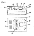
- Fig. 9 shows a radio-frequency (RF) hybrid switch module in accordance with a fourth exemplary embodiment.
- bump 31 of SAW filter chip 20 is electrically connected to a pad provided on laminated body 18 by flip chip bonding.
- a space between SAW filter chip 20 and laminated body 18 is filled with sealing resin 32 for covering a connection between bump 31 and the pad.
- the resin seals the periphery of this connection hermetically without contacting cap 26.
- An elastic surface portion of SAW filter chip 20 is provided with micro-cavity 27 and a cover defining a cavity similarly to the modules shown in Figs. 5 and 6, thereby being hermetically sealed without interfering with elastic vibration occurring at the elastic surface portion.
- bare-chip diode 30 may be coated with sealing resin 32.
- the RF hybrid switch module of the fourth embodiment has a smaller size and a lower profile than a conventional module and can be manufactured inexpensively since this module does not require an alumina package.
- plate-like laminated body 18 is divided into an area for SAW filter chip 20 and an area for chip devices 23, 24, thus allowing only the area for chip devices, for example, to have soldering paste printed thereon, to be subjected to reflow, and to be cleaned. This facilitates the mounting of the chip devices and enhances cost reduction of the module.
- the similar advantages can be obtained even when a semiconductor switching, e.g. a field effect transistor, is - used instead of bare-chip diode 30.
- a GSM/DCS dual-band device is explained.
- the present invention is not limited to this and may be applicable to, for example, single-band and triple-band devices.
- the number of chip devices and the number of SAW filter chips that have been illustrated in the first to fourth embodiments do not restrict the technique of the present invention.
- the same advantages can be obtained from, for example, a module including no chip device.
- the module may not include cap 26.
- the laminated body of the RF hybrid switch module in accordance with each of the first to fourth embodiments may include a thin ceramic substrate previously sintered and smoothed at its surface to which the SAW filter is mounted. Specifically, plural yet-to-be-sintered green sheets are affixed to the ceramic substrate, and a conductive pattern is printed on or transferred to the green sheet for forming a circuit. The resultant laminated body is thereafter sintered and then having the SAW filter mounted thereon. In this way, the SAW filter can be mounted to the smooth surface of the previously-sintered ceramic substrate, and this provides the module with extremely high reliability. Alumina, forsterite or the like is usable for the ceramic substrate.
- the green sheet upon being made of material sintered at a low temperature, allows material having a low resistance, e.g. silver and copper, to be used for the conductive pattern forming the circuit, and this reduces loss in the circuit.
- an elastic surface portion for generating a surface acoustic wave is provided with a cavity and is hermetically sealed.
- a surface acoustic wave filter can be mounted on a laminated body similarly to other chip devices. This allows the module to have an extremely small size and a low-profile.
Landscapes
- Engineering & Computer Science (AREA)
- Computer Networks & Wireless Communication (AREA)
- Signal Processing (AREA)
- Surface Acoustic Wave Elements And Circuit Networks Thereof (AREA)
- Transceivers (AREA)
- Electronic Switches (AREA)
Abstract
A small radio-frequency hybrid switch module is provided for switching
between transmitted signals and received signals in plural frequency bands.
This module includes: a laminated body including a dielectric layer; a diplexer;
a switching circuit; a low pass filter (LPF); a conductive pattern provided on
the dielectric layer for forming at least one of the diplexer, the switching
circuit and the LPF; a surface acoustic wave (SAW) filter mounted on the
laminated body; a cover provided on the SAW filter for forming a cavity which
allows surface acoustic wave vibration and for hermetically sealing the cavity;
and a semiconductor switching device mounted on the laminated body for
forming a part of the switching circuit.
Description
The present invention relates to a radio-frequency hybrid switch
module for use in mobile communications equipment including a mobile
phone.
Fig. 1 is a circuit block diagram of an antenna duplexer used in a
GSMIDCS dual-band mobile phone conforming to European standards for
mobile communications based on a Time Division Multiple Access system.
The antenna duplexer includes antenna terminal 1, GSM-band transmitting
(GSM-TX) terminal 2, GSM-band receiving (GSM-RX) terminal 3, DCS-band
transmitting (DCS-TX) terminal 4, DCS-band receiving (DCS-RX) terminal 5,
diplexer 6 for separating and combining frequency components in GSM and
DCS bands, switches 7, 8 for switching between transmission and reception,
low pass filters (LPFs) 9, 11 for removing unwanted harmonic signals, and
surface acoustic wave (SAW) filters 10, 12 for allowing a band of received
frequencies to pass.
Fig. 10 shows a structure of a conventional antenna duplexer. This
antenna duplexer includes ceramic multi-layer substrate 18, alumina package
19, SAW device chip 20, bonding wire 21, lid 22 of alumina package 19, diodes
23 functioning as switching devices, chip devices 24, pad 25 formed on the
alumina package for wire bonding, and metal cap 26. Ceramic multi-layer
substrate 18 includes a LPF and a diplexer formed therein.
In the duplexer described above, SAW chip 20 is put in alumina package
19 and mounted over ceramic multi-layer substrate 18. Alumina package 19,
for being sealed hermetically with lid 22, needs to has a wall thickness 19a
ranging from about 0.5mm to 1.0mm, Thus hardly having a reduced size.
A small radio-frequency (RF) hybrid switch module is provided for
switching between transmit-signals and receive-signals in plural frequency
bands.
This module includes: a laminated body having a dielectric layer; a
diplexer; a switching circuit; a low pass filter (LPF); a conductive pattern on
the dielectric layer for forming at least one of the diplexer, the switching
circuit and the LPF; a surface acoustic wave (SAW) filter mounted on the
laminated body; a cover on the SAW filter for forming a cavity which allows
surface acoustic wave vibration and hermetically sealing the cavity; and a
semiconductor switching device mounted on the laminated body for forming a
part of the switching circuit.
Figs. 1-4 are circuit block diagrams each illustrating a radio-frequency
(RF) hybrid switch module for a GSM/DCS mobile phone conforming with
European standards for mobile communications. The module includes switch
13 for switching between transmission and reception in GSM and DCS bands,
diplexers 14, 15, low pass filters (LPFs) 9, 11 for removing harmonics, and
SP4T switch 17.
In the circuit illustrated by Fig. 1, antenna terminal 1 is connected to
diplexer 6 which separates and combines signals in the GSM and DCS bands.
Respective terminals for the GSM and DCS bands of diplexer 6 are connected
to switches 7 and 8, respectively. Transmitting sides of switches 7, 8 are
connected to LPFs 9, 11, respectively, while receiving sides of switches 7, 8 are
connected to surface acoustic wave (SAW) filters 10, 12, respectively. Filters
9,10,11,12 are connected to terminals 2, 3, 4 and 5, respectively.
In the circuit illustrated by Fig. 2, an antenna terminal is connected to
switch 13. Switch 13 separates signals into transmitted signals and received
signals. Diplexers 14, 15 separate and combine the signals in the GSM and
DCS bands. Transmitting terminals of diplexer 14 are connected to LPFs 9
and 11, respectively, while receiving terminals of diplexer 15 are connected to
SAW filters 10 and 12, respectively. Filters 9, 10, 11, 12 are connected to
terminals 2, 3, 4 and 5, respectively.
In the circuit illustrated by Fig. 3, LPF 16 for removing a harmonic
component from a transmitted signal is connected to antenna terminal 1.
SP4T switch 17 allocates the transmitted signals and received signals among
terminals 2, 3, 4, and 5. Receiving terminals of switch 17 are coupled to
terminals 3, 5 via SAW filters 10, 12, respectively.
In the circuit illustrated by Fig. 4, SP4T switch 17 is connected to
antenna terminal 1. Transmitting terminals of switch 17 are connected to
LPFs 9, 11, respectively, while receiving terminals of switch 17 are connected
to SAW filters 10, 12, respectively. Filters 9, 11, 10, 12 are connected to
terminals 2, 3, 4 and 5, respectively.
In the circuits described above, switches 7, 8, 13, 17 are each formed of a
semiconductor switching device; e.g. a diode or a field effect transistor. LPFs
9, 11, 16 and diplexers 6, 14, 15 are formed of a conductive pattern provided on
a dielectric layer. This dielectric layer and other dielectric layer form a
laminated body.
Fig. 5 shows an RF hybrid switch module in accordance with the first
embodiment. The module includes cover (hereinafter referred to as "micro-cavity")
27 defining a cavity at an elastic vibrating portion of SAW filter chip
20, potting resin 28, and pad 29 formed on laminated body 18 for wire bonding.
In the first embodiment, the elastic surface portion of SAW filter chip 20
is formed with micro-cavity 27and fortified with potting resin 28, thereby
being hermetically sealed over laminated body 18 without interfering an
elastic vibration. Chip devices 23, 24 are mounted next to chip 20.
Consequently, the module of this embodiment has a smaller size and a
lower profile than a conventional module and can be manufactured
inexpensively since this module does not require an alumina package.
Further, The plate-like laminated body 18 may be divided into an area for
SAW filter chip 20 and an area for chip devices 23, 24, thus allowing only the
area for the chip devices, for example, to have soldering paste printed thereon,
to be subjected to reflow, and to be cleaned. This facilitates the chip devices
to be mounted easily and enhances cost reduction of the module.
Fig. 6 shows a radio-frequency hybrid switch module in accordance with
a second exemplary embodiment of the present invention. An elastic surface
portion of SAW filter chip 20 is provided with micro-cavity 27, a cover defining
a cavity. Micro-cavity 27 is fortified with potting resin 28 as in the module
shown in Fig. 5, thus allowing the elastic surface portion to be hermetically
sealed over laminated body 18 without interfering with elastic vibration.
Bare-chip diode 30 is mounted on laminated body 18 similarly to SAW filter
chip 20 and coated with potting resin 28.
Therefore, the module of the present embodiment has a smaller size and
a lower profile than a conventional module and can be manufactured
inexpensively since this module does not require an alumina package.
Further, plate-like laminated body 18 is divided into an area for SAW filter
chip 20 and an area for chip devices 23, 24 thus allowing only the area for the
chip devices, for example, to have soldering paste printed thereon, to be
subjected to reflow, and to be cleaned. This facilitates the chip devices to be
mounted easily and enhances cost reduction of the module. The similar
advantages are obtainable even if a semiconductor switching device, e.g. a
field effect transistor, is used instead of bare-chip diode 30.
As shown in Fig. 7, wall 33 made of resin may be provided on the
periphery of the bare chips on the laminated body. Wall 33 is taller than the
bare chips. The bare chips placed across wall 33 from the chip devices may be
covered with the potting resin. Thus, the potting resin is prevented from
flowing into a region not requiring the potting resin, and a region to be covered
with the potting resin is limited. Accordingly, a clearance for an overflowing
potting resin can be minimized, and this reduces the size of the module easily
and improves production yield of the module.
As shown in Fig. 6, at least one of the SAW filter and the bare chip is
disposed on one side of the laminated body. In other words, the bare chips are
separated from the chip devices on the laminated body by being disposed in
the area positioned in horizontal or vertical relation to the area for the chip
devices. This allows the module to be manufactured since soldering paste can
be applied to laminated body 18 by thick film printing to solder the chip
devices, and since flux can be cleaned efficiently after the soldering.
The potting resin may cover the entire surface of the laminated body on
which the chips and the chip devices are mounted. This improves mechanical
reliability of the module. In addition, the module can be manufactured easily
and inexpensively since a region (not shown) to be coated with the potting
resin need not be specifically restricted.
Fig. 8 shows a radio-frequency (RF) hybrid switch module in accordance
with a third exemplary embodiment. The module includes bump 31 and
sealing resin 32. Bump 31 functioning as an electrode for SAW filter chip 20
is electrically connected to a pad provided on laminated body 18 by flip chip
bonding. A space between SAW filter chip 20 and laminated body 18 is filled
with sealing resin 32 for covering a connection between bump 31 and the pad.
This seals the periphery of this connection hermetically without contacting
cap 26. An elastic surface portion of SAW filter chip 20 is provided with
micro-cavity 27, a cover defining a cavity similarly to the modules shown in
Figs. 5 and 6, thus being hermetically sealed without interfering with elastic
vibration at the elastic surface portion.
The RF hybrid switch module of the present embodiment has a smaller
size and a lower profile than a conventional module, and can be made
inexpensively since this module does not require an alumina package.
Further, plate-like laminated body 18 is divided into an area for SAW filter
chip 20 and an area for chip devices 23, 24, thus allowing only the area for chip
devices, for example, to have soldering paste printed thereon, to be subjected
to reflow, and to be cleaned. This facilitates the mounting of the chip devices
and enhances cost reduction of the module.
Fig. 9 shows a radio-frequency (RF) hybrid switch module in accordance
with a fourth exemplary embodiment. In this module, bump 31 of SAW filter
chip 20 is electrically connected to a pad provided on laminated body 18 by flip
chip bonding. A space between SAW filter chip 20 and laminated body 18 is
filled with sealing resin 32 for covering a connection between bump 31 and the
pad. The resin seals the periphery of this connection hermetically without
contacting cap 26. An elastic surface portion of SAW filter chip 20 is provided
with micro-cavity 27 and a cover defining a cavity similarly to the modules
shown in Figs. 5 and 6, thereby being hermetically sealed without interfering
with elastic vibration occurring at the elastic surface portion. Together with
the SAW filter chip, bare-chip diode 30 may be coated with sealing resin 32.
The RF hybrid switch module of the fourth embodiment has a smaller
size and a lower profile than a conventional module and can be manufactured
inexpensively since this module does not require an alumina package.
Further, plate-like laminated body 18 is divided into an area for SAW filter
chip 20 and an area for chip devices 23, 24, thus allowing only the area for chip
devices, for example, to have soldering paste printed thereon, to be subjected
to reflow, and to be cleaned. This facilitates the mounting of the chip devices
and enhances cost reduction of the module. The similar advantages can be
obtained even when a semiconductor switching, e.g. a field effect transistor, is
- used instead of bare-chip diode 30.
In the first to fourth embodiments, a GSM/DCS dual-band device is
explained. However, the present invention is not limited to this and may be
applicable to, for example, single-band and triple-band devices.
The number of chip devices and the number of SAW filter chips that
have been illustrated in the first to fourth embodiments do not restrict the
technique of the present invention. The same advantages can be obtained
from, for example, a module including no chip device. In addition, the module
may not include cap 26.
The laminated body of the RF hybrid switch module in accordance with
each of the first to fourth embodiments may include a thin ceramic substrate
previously sintered and smoothed at its surface to which the SAW filter is
mounted. Specifically, plural yet-to-be-sintered green sheets are affixed to
the ceramic substrate, and a conductive pattern is printed on or transferred to
the green sheet for forming a circuit. The resultant laminated body is
thereafter sintered and then having the SAW filter mounted thereon. In this
way, the SAW filter can be mounted to the smooth surface of the previously-sintered
ceramic substrate, and this provides the module with extremely high
reliability. Alumina, forsterite or the like is usable for the ceramic substrate.
The green sheet, upon being made of material sintered at a low temperature,
allows material having a low resistance, e.g. silver and copper, to be used for
the conductive pattern forming the circuit, and this reduces loss in the circuit.
In a radio-frequency hybrid switch module of the present invention, an
elastic surface portion for generating a surface acoustic wave is provided with
a cavity and is hermetically sealed. Thus, a surface acoustic wave filter can
be mounted on a laminated body similarly to other chip devices. This allows
the module to have an extremely small size and a low-profile.
Claims (10)
- A radio-frequency (RF) hybrid switch module comprising:a laminated body including a dielectric layer;a diplexer;a switching circuit;a low pass filter (LPF);a conductive pattern on sold dielectric layer, for forming at least one of said diplexer, said switching circuit, and said LPF;a surface acoustic wave (SAW) filter mounted on said laminated body;a cover on said SAW filter, for forming a cavity which allows surface acoustic wave vibration and for hermetically sealing said cavity; anda semiconductor switching device mounted on said laminated body, for forming a part of said switching circuit.
- The RF hybrid switch module of claim 1. further comprising:a pad provided on said laminated body;a bonding wire connecting said SAW filter to said pad; anda potting resin covering said electrode part, said bonding wire, and said SAW filter.
- The RF hybrid switch module of claim 2,
wherein said semiconductor switching device is a bare chip, and
wherein said potting resin covers said bare chip. - The RF hybrid switch module of claim 3, further comprising:wherein said potting resin covers said bare chip from said wall.a wall provided at a periphery of said bare chip on said laminated body, said wall being taller than said bare chip,
- The RF hybrid switch module of claim 2, further comprising:wherein a position for at least one of said SAW filter and said bare chip and a position for said chip device are mounted in respective two regions separated from each other on said laminated body.a chip device included in at least one of said diplexer, said switching circuit and said LPF, said chip device being mounted on said laminated body,
- The RF hybrid switch module of claim 2, wherein said potting resin covers substantially an entire surface of said laminated body including said semiconductor switching device and said SAW filter mounted thereon
- The RF hybrid switch module of claim 1, further comprising a potting resin for covering substantially an entire surface of said laminated body including said semiconductor switching device and said SAW filter mounted thereon.
- The RF hybrid switch module of claim 1, further comprising:a pad provided on said laminated body;a bump provided at said SAW filter for electrically connecting said SAW filter to said pad by flip chip bonding; anda potting resin with which a space between said SAW filter and said laminated body is filled for covering said pad and said bump.
- The RF hybrid switch module of claim 1, wherein said laminated body further includes a ceramic substrate on which said SAW filter is mounted.
- A method of manufacturing a radio-frequency hybrid switch module including a laminated body having a dielectric layer, a conductive pattern provided on the dielectric layer, and a surface acoustic wave (SAW) filter mounted on the laminated body, said method comprising the steps of:forming the conductive pattern on a green sheet by one of printing and transferring;affixing the green sheet to a sintered ceramic substrate;sintering the ceramic substrate and the green sheet to form the laminated body; andmounting the SAW filter on the ceramic sheet.
Applications Claiming Priority (3)
| Application Number | Priority Date | Filing Date | Title |
|---|---|---|---|
| JP2000307276A JP2002118487A (en) | 2000-10-06 | 2000-10-06 | High frequency composite switch module |
| JP2000307276 | 2000-10-06 | ||
| PCT/JP2001/008792 WO2002032001A1 (en) | 2000-10-06 | 2001-10-05 | High-frequency composite switch module |
Publications (2)
| Publication Number | Publication Date |
|---|---|
| EP1233528A1 true EP1233528A1 (en) | 2002-08-21 |
| EP1233528A4 EP1233528A4 (en) | 2009-07-22 |
Family
ID=18787813
Family Applications (1)
| Application Number | Title | Priority Date | Filing Date |
|---|---|---|---|
| EP01974706A Withdrawn EP1233528A4 (en) | 2000-10-06 | 2001-10-05 | HIGH FREQUENCY COMPOSITE SWITCHING MODULE |
Country Status (4)
| Country | Link |
|---|---|
| US (1) | US6759925B2 (en) |
| EP (1) | EP1233528A4 (en) |
| JP (1) | JP2002118487A (en) |
| WO (1) | WO2002032001A1 (en) |
Cited By (5)
| Publication number | Priority date | Publication date | Assignee | Title |
|---|---|---|---|---|
| WO2004100387A1 (en) * | 2003-05-12 | 2004-11-18 | Epcos Ag | Low-loss transmitter module |
| WO2004051745A3 (en) * | 2002-12-05 | 2005-02-24 | Epcos Ag | Electronic component comprising a plurality of chips and method for producing the same |
| EP1699277A4 (en) * | 2003-12-26 | 2007-08-15 | Murata Manufacturing Co | CERAMIC MULTILAYER SUBSTRATE |
| US8014731B2 (en) | 2001-01-18 | 2011-09-06 | Epcos Ag | Electric circuit module, circuit module arrangement and use of said circuit module and of said circuit module arrangement |
| US8116046B2 (en) | 2002-10-02 | 2012-02-14 | Epcos Ag | Circuit arrangement that includes a device to protect against electrostatic discharge |
Families Citing this family (25)
| Publication number | Priority date | Publication date | Assignee | Title |
|---|---|---|---|---|
| JP2002204135A (en) * | 2000-12-28 | 2002-07-19 | Matsushita Electric Ind Co Ltd | High frequency low pass filter |
| JP2003087150A (en) * | 2001-09-14 | 2003-03-20 | Matsushita Electric Ind Co Ltd | High frequency composite switch module |
| EP1341317A1 (en) * | 2001-09-21 | 2003-09-03 | Matsushita Electric Industrial Co., Ltd. | High-frequency device |
| US20050059371A1 (en) * | 2001-09-28 | 2005-03-17 | Christian Block | Circuit arrangement, switching module comprising said circuit arrangement and use of switching module |
| US7492565B2 (en) | 2001-09-28 | 2009-02-17 | Epcos Ag | Bandpass filter electrostatic discharge protection device |
| JP3789410B2 (en) | 2002-08-29 | 2006-06-21 | 富士通メディアデバイス株式会社 | Surface mount electronic component module and method for manufacturing the same |
| EP1537677A1 (en) * | 2002-08-29 | 2005-06-08 | Koninklijke Philips Electronics N.V. | Transceiver apparatus for use in a multi-frequency communication system, base station of a multi-frequency communication system, method for use of the transceiver apparatus, method of transceiving a multi-frequency signal in a multi-frequency communication system |
| KR100548244B1 (en) | 2003-03-14 | 2006-02-02 | 엘지전자 주식회사 | Low cost active smart antenna system and its manufacturing method |
| JP2005064780A (en) * | 2003-08-11 | 2005-03-10 | Fdk Corp | High frequency switch circuit |
| TW200520201A (en) | 2003-10-08 | 2005-06-16 | Kyocera Corp | High-frequency module and communication apparatus |
| EP1696579B1 (en) * | 2003-12-11 | 2013-02-20 | Hitachi Metals, Ltd. | Multi-band high-frequency circuit, multi-band high-frequency circuit part, and multi-band communication device using the same |
| JP4678572B2 (en) * | 2004-05-20 | 2011-04-27 | 日立金属株式会社 | Multilayer balun transformer and high-frequency switch module using the same |
| JP4678571B2 (en) * | 2004-05-20 | 2011-04-27 | 日立金属株式会社 | Multilayer balun transformer and high-frequency switch module using the same |
| JP4134129B2 (en) | 2004-10-28 | 2008-08-13 | Tdk株式会社 | High frequency module |
| CN1767406B (en) * | 2004-10-28 | 2010-06-16 | Tdk株式会社 | High frequency module |
| JP4134005B2 (en) | 2004-11-15 | 2008-08-13 | Tdk株式会社 | High frequency module |
| US8131226B1 (en) | 2004-12-13 | 2012-03-06 | Hitachi Metals, Ltd. | Multi-band-high-frequency circuit, multi-band high-frequency circuit component and multi-band communication apparatus using same |
| JP2007318657A (en) * | 2006-05-29 | 2007-12-06 | Murata Mfg Co Ltd | Transmitter |
| JP5041285B2 (en) * | 2007-04-24 | 2012-10-03 | 日立金属株式会社 | High frequency components |
| JP2009021895A (en) * | 2007-07-13 | 2009-01-29 | Panasonic Corp | Antenna duplexer and communication equipment using it |
| DE102012001346A1 (en) * | 2012-01-24 | 2013-07-25 | Giesecke & Devrient Gmbh | Method for producing a data carrier |
| GB2526197B (en) * | 2014-04-11 | 2020-11-18 | Skyworks Solutions Inc | Circuits and methods related to radio-frequency receivers having carrier aggregation |
| US10447411B2 (en) * | 2015-08-25 | 2019-10-15 | Samsung Electro-Mechanics Co., Ltd. | Acoustic wave device and method of manufacturing the same |
| US10510694B2 (en) * | 2018-04-18 | 2019-12-17 | Analog Devices, Inc. | Radio frequency communication systems |
| WO2022209737A1 (en) * | 2021-03-31 | 2022-10-06 | 株式会社村田製作所 | High frequency module and communication device |
Family Cites Families (14)
| Publication number | Priority date | Publication date | Assignee | Title |
|---|---|---|---|---|
| JPS6297418A (en) * | 1985-10-23 | 1987-05-06 | Clarion Co Ltd | Packaging method for surface acoustic wave device |
| JPH084238B2 (en) * | 1986-01-24 | 1996-01-17 | 株式会社日立製作所 | Surface acoustic wave demultiplexer module and radio |
| JPH088605A (en) | 1994-06-20 | 1996-01-12 | Matsushita Electric Ind Co Ltd | Multilayer dielectric filter |
| JPH09232351A (en) * | 1996-02-23 | 1997-09-05 | Fujitsu Ltd | Electronic device package |
| DE69718693T2 (en) * | 1996-03-08 | 2003-11-27 | Matsushita Electric Industrial Co., Ltd. | Electronic component and manufacturing process |
| JP3329175B2 (en) * | 1996-03-11 | 2002-09-30 | 松下電器産業株式会社 | Surface acoustic wave device and method of manufacturing the same |
| JPH1093383A (en) | 1996-05-15 | 1998-04-10 | Matsushita Electric Ind Co Ltd | Surface acoustic wave device and method of manufacturing the same |
| JPH1032521A (en) * | 1996-07-17 | 1998-02-03 | Murata Mfg Co Ltd | Duplexer |
| JPH11127055A (en) * | 1997-10-23 | 1999-05-11 | Murata Mfg Co Ltd | Composite electronic components |
| JPH11154804A (en) * | 1997-11-20 | 1999-06-08 | Hitachi Ltd | High frequency circuit device |
| JP3484090B2 (en) * | 1998-12-22 | 2004-01-06 | 株式会社日立製作所 | Switched antenna duplexer and mobile radio terminal |
| JP2001102957A (en) * | 1999-09-28 | 2001-04-13 | Murata Mfg Co Ltd | Composite high-frequency component and mobile communication device using same |
| US6456172B1 (en) * | 1999-10-21 | 2002-09-24 | Matsushita Electric Industrial Co., Ltd. | Multilayered ceramic RF device |
| US6570469B2 (en) * | 2000-06-27 | 2003-05-27 | Matsushita Electric Industrial Co., Ltd. | Multilayer ceramic device including two ceramic layers with multilayer circuit patterns that can support semiconductor and saw chips |
-
2000
- 2000-10-06 JP JP2000307276A patent/JP2002118487A/en active Pending
-
2001
- 2001-10-05 EP EP01974706A patent/EP1233528A4/en not_active Withdrawn
- 2001-10-05 US US10/148,702 patent/US6759925B2/en not_active Expired - Fee Related
- 2001-10-05 WO PCT/JP2001/008792 patent/WO2002032001A1/en not_active Ceased
Cited By (6)
| Publication number | Priority date | Publication date | Assignee | Title |
|---|---|---|---|---|
| US8014731B2 (en) | 2001-01-18 | 2011-09-06 | Epcos Ag | Electric circuit module, circuit module arrangement and use of said circuit module and of said circuit module arrangement |
| US8116046B2 (en) | 2002-10-02 | 2012-02-14 | Epcos Ag | Circuit arrangement that includes a device to protect against electrostatic discharge |
| WO2004051745A3 (en) * | 2002-12-05 | 2005-02-24 | Epcos Ag | Electronic component comprising a plurality of chips and method for producing the same |
| WO2004100387A1 (en) * | 2003-05-12 | 2004-11-18 | Epcos Ag | Low-loss transmitter module |
| US7454178B2 (en) | 2003-05-12 | 2008-11-18 | Epcos Ag | Low-loss transmitter module |
| EP1699277A4 (en) * | 2003-12-26 | 2007-08-15 | Murata Manufacturing Co | CERAMIC MULTILAYER SUBSTRATE |
Also Published As
| Publication number | Publication date |
|---|---|
| US20030048154A1 (en) | 2003-03-13 |
| EP1233528A4 (en) | 2009-07-22 |
| US6759925B2 (en) | 2004-07-06 |
| WO2002032001A1 (en) | 2002-04-18 |
| JP2002118487A (en) | 2002-04-19 |
Similar Documents
| Publication | Publication Date | Title |
|---|---|---|
| US6759925B2 (en) | Radio-frequency hybrid switch module | |
| CN103813635A (en) | High frequency circuit module | |
| EP1381258A1 (en) | High-frequency module | |
| US9070963B2 (en) | Duplexer | |
| US7315455B2 (en) | Surface-mounted electronic component module and method for manufacturing the same | |
| US9007146B2 (en) | Duplexer | |
| US11871508B2 (en) | Radio-frequency module and communication device | |
| US11546003B2 (en) | Radio frequency module and communication device | |
| KR102737270B1 (en) | Radio-frequency module and communications device | |
| US20060194370A1 (en) | Radio frequency module and fabrication method thereof | |
| JP2000059174A (en) | Surface acoustic wave duplexer and mobile communication device using the same | |
| US20240292519A1 (en) | High frequency module and communication device | |
| CN100378967C (en) | Ceramic package and manufacturing method thereof | |
| JP2006135771A (en) | Electronic component module | |
| JP2008271169A (en) | High frequency module and portable terminal equipped with the same | |
| KR100820556B1 (en) | Duplexer manufacturing method | |
| JP2004235877A (en) | High frequency module | |
| JP2002261581A (en) | High frequency module components | |
| JP2002094410A (en) | Antenna switch module with SAW filter | |
| JP2005136887A (en) | High frequency module and wireless communication device | |
| US12336156B2 (en) | Radio frequency module and communication device | |
| US12426223B2 (en) | Radio frequency module and communication device | |
| US20240048173A1 (en) | High frequency module and communication apparatus | |
| JP4331634B2 (en) | Antenna switching module and manufacturing method thereof | |
| JP2025097073A (en) | High frequency module and communication device |
Legal Events
| Date | Code | Title | Description |
|---|---|---|---|
| PUAI | Public reference made under article 153(3) epc to a published international application that has entered the european phase |
Free format text: ORIGINAL CODE: 0009012 |
|
| 17P | Request for examination filed |
Effective date: 20020528 |
|
| AK | Designated contracting states |
Kind code of ref document: A1 Designated state(s): AT BE CH CY DE DK ES FI FR GB GR IE IT LI LU MC NL PT SE TR |
|
| RBV | Designated contracting states (corrected) |
Designated state(s): AT BE CH DE FR GB LI |
|
| RAP1 | Party data changed (applicant data changed or rights of an application transferred) |
Owner name: PANASONIC CORPORATION |
|
| A4 | Supplementary search report drawn up and despatched |
Effective date: 20090622 |
|
| STAA | Information on the status of an ep patent application or granted ep patent |
Free format text: STATUS: THE APPLICATION IS DEEMED TO BE WITHDRAWN |
|
| 18D | Application deemed to be withdrawn |
Effective date: 20090922 |