EP1233474A2 - Elektrische Verbindungseinrichtung und Verfahren für flache Schatungen - Google Patents
Elektrische Verbindungseinrichtung und Verfahren für flache Schatungen Download PDFInfo
- Publication number
- EP1233474A2 EP1233474A2 EP02001485A EP02001485A EP1233474A2 EP 1233474 A2 EP1233474 A2 EP 1233474A2 EP 02001485 A EP02001485 A EP 02001485A EP 02001485 A EP02001485 A EP 02001485A EP 1233474 A2 EP1233474 A2 EP 1233474A2
- Authority
- EP
- European Patent Office
- Prior art keywords
- cover
- conductor
- terminal
- flat circuit
- circuit
- Prior art date
- Legal status (The legal status is an assumption and is not a legal conclusion. Google has not performed a legal analysis and makes no representation as to the accuracy of the status listed.)
- Withdrawn
Links
Images


Classifications
-
- H—ELECTRICITY
- H04—ELECTRIC COMMUNICATION TECHNIQUE
- H04M—TELEPHONIC COMMUNICATION
- H04M1/00—Substation equipment, e.g. for use by subscribers
- H04M1/02—Constructional features of telephone sets
- H04M1/0202—Portable telephone sets, e.g. cordless phones, mobile phones or bar type handsets
- H04M1/0206—Portable telephones comprising a plurality of mechanically joined movable body parts, e.g. hinged housings
- H04M1/0208—Portable telephones comprising a plurality of mechanically joined movable body parts, e.g. hinged housings characterized by the relative motions of the body parts
- H04M1/0214—Foldable telephones, i.e. with body parts pivoting to an open position around an axis parallel to the plane they define in closed position
- H04M1/0216—Foldable in one direction, i.e. using a one degree of freedom hinge
-
- H—ELECTRICITY
- H01—ELECTRIC ELEMENTS
- H01R—ELECTRICALLY-CONDUCTIVE CONNECTIONS; STRUCTURAL ASSOCIATIONS OF A PLURALITY OF MUTUALLY-INSULATED ELECTRICAL CONNECTING ELEMENTS; COUPLING DEVICES; CURRENT COLLECTORS
- H01R12/00—Structural associations of a plurality of mutually-insulated electrical connecting elements, specially adapted for printed circuits, e.g. printed circuit boards [PCB], flat or ribbon cables, or like generally planar structures, e.g. terminal strips, terminal blocks; Coupling devices specially adapted for printed circuits, flat or ribbon cables, or like generally planar structures; Terminals specially adapted for contact with, or insertion into, printed circuits, flat or ribbon cables, or like generally planar structures
- H01R12/50—Fixed connections
- H01R12/59—Fixed connections for flexible printed circuits, flat or ribbon cables or like structures
- H01R12/65—Fixed connections for flexible printed circuits, flat or ribbon cables or like structures characterised by the terminal
- H01R12/69—Fixed connections for flexible printed circuits, flat or ribbon cables or like structures characterised by the terminal deformable terminals, e.g. crimping terminals
-
- H—ELECTRICITY
- H05—ELECTRIC TECHNIQUES NOT OTHERWISE PROVIDED FOR
- H05K—PRINTED CIRCUITS; CASINGS OR CONSTRUCTIONAL DETAILS OF ELECTRIC APPARATUS; MANUFACTURE OF ASSEMBLAGES OF ELECTRICAL COMPONENTS
- H05K3/00—Apparatus or processes for manufacturing printed circuits
- H05K3/30—Assembling printed circuits with electric components, e.g. with resistors
- H05K3/32—Assembling printed circuits with electric components, e.g. with resistors electrically connecting electric components or wires to printed circuits
- H05K3/325—Assembling printed circuits with electric components, e.g. with resistors electrically connecting electric components or wires to printed circuits by abutting or pinching; Mechanical auxiliary parts therefor
- H05K3/326—Assembling printed circuits with electric components, e.g. with resistors electrically connecting electric components or wires to printed circuits by abutting or pinching; Mechanical auxiliary parts therefor the printed circuit having integral resilient or deformable parts, e.g. tabs or parts of flexible circuits
-
- H—ELECTRICITY
- H01—ELECTRIC ELEMENTS
- H01R—ELECTRICALLY-CONDUCTIVE CONNECTIONS; STRUCTURAL ASSOCIATIONS OF A PLURALITY OF MUTUALLY-INSULATED ELECTRICAL CONNECTING ELEMENTS; COUPLING DEVICES; CURRENT COLLECTORS
- H01R2201/00—Connectors or connections adapted for particular applications
- H01R2201/16—Connectors or connections adapted for particular applications for telephony
-
- H—ELECTRICITY
- H05—ELECTRIC TECHNIQUES NOT OTHERWISE PROVIDED FOR
- H05K—PRINTED CIRCUITS; CASINGS OR CONSTRUCTIONAL DETAILS OF ELECTRIC APPARATUS; MANUFACTURE OF ASSEMBLAGES OF ELECTRICAL COMPONENTS
- H05K1/00—Printed circuits
- H05K1/02—Details
- H05K1/11—Printed elements for providing electric connections to or between printed circuits
- H05K1/118—Printed elements for providing electric connections to or between printed circuits specially for flexible printed circuits, e.g. using folded portions
-
- H—ELECTRICITY
- H05—ELECTRIC TECHNIQUES NOT OTHERWISE PROVIDED FOR
- H05K—PRINTED CIRCUITS; CASINGS OR CONSTRUCTIONAL DETAILS OF ELECTRIC APPARATUS; MANUFACTURE OF ASSEMBLAGES OF ELECTRICAL COMPONENTS
- H05K3/00—Apparatus or processes for manufacturing printed circuits
- H05K3/0058—Laminating printed circuit boards onto other substrates, e.g. metallic substrates
Definitions
- This invention generally relates to a system and method for providing an electrical connection with a flat circuit, such as in a cover assembly for a mobile telephone.
- a flat flexible circuit conventionally includes an elongated flat flexible dielectric substrate having a pattern of conductors on one or both sides thereof.
- the conductors may be covered with a thin, flexible protective layer or film on one or both sides of the circuit. If protective layers or films are used, cutouts are formed to expose the underlying conductors where the conductors are to engage the conductors or terminals of a complementary connecting device which may be a second flat circuit, a printed circuit board, discrete electrical wires or the terminals of a complementary connector.
- flat flexible circuits are supported on some form of generally rigid dielectric support structure. This enables the flexible circuit to be mounted or supported in a given apparatus, and the conductors are easier to be terminated or electrically connected to the conductors or terminals of the complementary connecting device.
- a connecting device such as a switch
- a switch located at the inside or bottom of the cover may be actuated in response to the cover moving between open and closed positions.
- the flat flexible cable is located on the opposite or top side of the cover.
- An object, therefore, of the invention is to provide a new and improved electrical connection system for a flat circuit.
- Another object of the invention is to provide a new and improved method for providing an electrical connection with a flat circuit.
- a further object of the invention is to provide a new and improved cover assembly for a mobile telephone.
- the system and method generally includes a rigid dielectric support structure, with a flat circuit on one side of the support structure.
- a terminal clip includes a contact portion at an opposite side of the support structure for electrically engaging a complementary connecting device.
- the terminal clip includes a shank portion extending from the contact portion through the support structure.
- a terminating portion is provided at an end of the shank portion at the one side of the support structure for termination to an appropriate conductor of the flat circuit.
- the system and method is disclosed in a cover assembly for a mobile telephone.
- the rigid dielectric support structure is a cover of the assembly, the cover having first and second sides with at least one aperture passing therethrough between the sides.
- the flat circuit is mounted on the first side of the cover.
- the contact portion of the terminal clip is located at the second side of the cover for engaging the complementary connecting device.
- the shank portion of the terminal clip extends from the contact portion through the aperture in the cover and is terminated to the conductor of the flat circuit.
- the contact portion of the terminal clip herein comprises a contact plate juxtaposed against the second side of the cover.
- the terminating portion of the terminal clip comprises a distal end of the shank portion bent into engagement with the conductor.
- the cover includes a pair of apertures, and the terminal is generally U-shaped with a pair of the shank portions extending from opposite ends of the contact portion through the pair of apertures.
- the flat circuit herein comprises a flat flexible circuit.
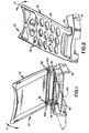
- the invention is embodied in a cover assembly, generally designated 10, for a mobile telephone.
- the cover assembly includes a base 12 appropriately mounted on the mobile telephone and a cover, generally designated 14, pivotally mounted on the base for movement in the direction of double-headed arrow "A" between a closed position and an open position (as shown).
- Base 12 mounts a pair of laterally spaced switches, generally designated 16, on the inside thereof Only the left-hand switch is visible in Figure 1. Nevertheless, each switch includes one or more upwardly extending, vertically reciprocating switch pins 18. In the industry, such switches commonly are called “pogo pin connectors".
- cover 14 includes a generally rigid top plate 20 which is hinged at 22 to base 12 for pivotal movement in the direction of double-headed arrow "A".
- the top plate has a plurality of apertures 24 which receive a plurality of dome-shaped push-buttons of a conventional keypad (not shown) mounted on the top of the cover.
- a generally rigid bottom support plate 26 (Fig. 3) is snap-fit into the underside of top plate 20.
- a flat flexible circuit 28 (Fig. 4) is sandwiched between top plate 20 (Fig. 2) and bottom support plate 26 (Fig. 3).
- the circuit has conductor pad arrays 29 for engagement by the push buttons of the keypad.
- FIG. 1 shows that a liquid crystal display (LCD) 30 is disposed on the upper portion of base 12.
- LCD liquid crystal display
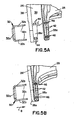
- Figures 5A-5E show the system and method for providing an electrical connection with or terminating flat circuit 28 on top of bottom support plate 26 so that the conductors thereof can be operative for engaging switch pins 18 at the bottom of the support plate beneath cover 14.
- the system includes the use of a plurality of terminal clips or terminals, generally designated 32, which are visible in Figures I and 4.
- bottom support plate 26 includes a pair of laterally spaced leg portions 26a (Figs. 3 and 4), one of which is shown in Figures 5A-5E.
- the bottom support plate and leg portions have a first or top side 36 (Fig. 5A) and a second or bottom side 38.
- Flat flexible circuit 28 is disposed on top side 36 of the support plate and includes leg portions 28a which are juxtaposed over leg portions 26a of the support plate.
- Flat flexible circuit 28 includes a pattern of conductors 40 (Fig. 4) with a pair of conductors 42 extending into each leg portion 28a as seen in Figure 5A. If flat flexible circuit 28 is provided with a protective layer or film, the film is removed to expose conductors 42 at the top of the circuit.
- Each leg portion 26a of support plate 26 includes two pairs of apertures 44 which are aligned with two pairs of holes 46 in leg portions 28a of flat circuit 28. Holes 46 extend through conductors 42 as clearly seen in Figures 5A-5E..
- each terminal clip or terminal 32 is generally U-shaped and includes a contact portion or section 32a in the form of a flat contact plate.
- a pair of shank portions or connecting sections 32b project from opposite ends of contact portion 32a.
- the shank portions terminate in distal ends 32c which will form terminating portions of the terminal, as will be seen below.
- cover 14 is shown in Figures 5A-5E, four terminals 32 are used with cover 14 as seen in Figures 1 and 4.
- One terminal is used for each of the two pairs of apertures 44 in support plate 26 and holes 46 in flat circuit 28 at each opposite side of the cover assembly.
- Flat flexible circuit 28 first is mounted or positioned onto top side 36 (Fig. 5A) of support plate 26 as seen in Figure 5B.
- the flat circuit may be appropriately adhered to the top side of the support plate, or the circuit may be press-fit within an array of ribs 50 (Fig. 4) projecting upwardly from the support plate.
- Terminals 32 then are assembled in the direction of arrow "B" (Fig. 5B) by inserting shank portions 32b first through apertures 44 in support plate 28 and then through holes 46 in flat circuit 28 until the shank portions extend completely through the assembly as shown by the one terminal in Figure 5C.
- flat flexible circuit 28 is mounted to a first or top side 36 of support plate 26, while terminals 32 are mounted through a second or bottom side 38 of the support plate.
- contact portions 32 of the terminals are located at the bottom of cover 14 as seen in Figure 1, notwithstanding the fact that fiat flexible circuit 28 is mounted on the top of support plate 26.
- conductors 40 (Fig. 4) can be operatively associated with the keypad of the mobile telephone through apertures 24 (Fig. 2) at the top of the cover assembly, while conductors 42 (Figs. 5A-5C) are operatively associated by terminals 32 through the cover assembly with switches 16 located at a completely opposite side of cover 14,
Landscapes
- Engineering & Computer Science (AREA)
- Metallurgy (AREA)
- Manufacturing & Machinery (AREA)
- Microelectronics & Electronic Packaging (AREA)
- Signal Processing (AREA)
- Telephone Set Structure (AREA)
- Multi-Conductor Connections (AREA)
- Casings For Electric Apparatus (AREA)
- Combinations Of Printed Boards (AREA)
- Mounting Of Printed Circuit Boards And The Like (AREA)
- Mobile Radio Communication Systems (AREA)
Applications Claiming Priority (2)
| Application Number | Priority Date | Filing Date | Title |
|---|---|---|---|
| US767185 | 2001-01-22 | ||
| US09/767,185 US6364668B1 (en) | 2001-01-22 | 2001-01-22 | Electrical connection system and method for flat circuits |
Publications (2)
| Publication Number | Publication Date |
|---|---|
| EP1233474A2 true EP1233474A2 (de) | 2002-08-21 |
| EP1233474A3 EP1233474A3 (de) | 2003-04-02 |
Family
ID=25078750
Family Applications (1)
| Application Number | Title | Priority Date | Filing Date |
|---|---|---|---|
| EP02001485A Withdrawn EP1233474A3 (de) | 2001-01-22 | 2002-01-22 | Elektrische Verbindungseinrichtung und Verfahren für flache Schatungen |
Country Status (4)
| Country | Link |
|---|---|
| US (1) | US6364668B1 (de) |
| EP (1) | EP1233474A3 (de) |
| JP (1) | JP3780961B2 (de) |
| TW (1) | TW585001B (de) |
Families Citing this family (1)
| Publication number | Priority date | Publication date | Assignee | Title |
|---|---|---|---|---|
| EP2375500A1 (de) * | 2010-03-04 | 2011-10-12 | Tyco Electronics Nederland B.V. | Skalierbares Kontaktelement für elektrische Steckverbinder |
Citations (1)
| Publication number | Priority date | Publication date | Assignee | Title |
|---|---|---|---|---|
| US3409857A (en) * | 1965-08-23 | 1968-11-05 | Amp Inc | Electrical connectors for terminating leads of micro-modular components or the like |
Family Cites Families (16)
| Publication number | Priority date | Publication date | Assignee | Title |
|---|---|---|---|---|
| US3395381A (en) | 1966-11-25 | 1968-07-30 | Amp Inc | Crimpable connecting device for flat conductor cable |
| BE757965A (fr) | 1969-11-06 | 1971-04-23 | Amp Inc | Connecteur electrique |
| US3697925A (en) | 1970-07-22 | 1972-10-10 | Amp Inc | Termination means for flat cable |
| US3703604A (en) | 1971-11-30 | 1972-11-21 | Amp Inc | Flat conductor transmission cable |
| GB1474249A (en) | 1974-01-09 | 1977-05-18 | Amp Inc | Electrical contact for flat conductor cable |
| US4066319A (en) | 1974-04-30 | 1978-01-03 | Elco Corporation | Method and apparatus for flat conductor cable termination |
| US3960430A (en) | 1974-10-29 | 1976-06-01 | Amp Incorporated | Flat wiring system and crimped connection |
| US4002393A (en) | 1974-12-05 | 1977-01-11 | Amp Incorporated | Contact means for flat conductor cable and method of connecting same |
| US3999826A (en) * | 1975-06-30 | 1976-12-28 | General Motors Corporation | Connector for flexible printed circuit |
| GB1528998A (en) | 1976-06-18 | 1978-10-18 | Pressac Ltd | Electrical connecting method |
| US4371225A (en) | 1980-07-31 | 1983-02-01 | Thomas & Betts Corporation | Electrical connector for terminating flat multiconductor cable |
| GB8703389D0 (en) * | 1987-02-13 | 1987-03-18 | Pressac Ltd | Electrical connector |
| US5195908A (en) | 1988-06-30 | 1993-03-23 | Sumitomo Wiring Systems, Ltd. | Multicircuit cable connector |
| US5634813A (en) | 1995-12-13 | 1997-06-03 | Molex Incorporated | Crimpable electrical terminal |
| US6038313A (en) * | 1997-11-20 | 2000-03-14 | Nortel Networks Corporation | Double sided keyboard for a telephone |
| JP2000260504A (ja) * | 1999-03-11 | 2000-09-22 | Jst Mfg Co Ltd | Fpc圧着端子及びこれを用いた芯線の圧着構造 |
-
2001
- 2001-01-22 US US09/767,185 patent/US6364668B1/en not_active Expired - Fee Related
-
2002
- 2002-01-22 JP JP2002050514A patent/JP3780961B2/ja not_active Expired - Fee Related
- 2002-01-22 EP EP02001485A patent/EP1233474A3/de not_active Withdrawn
- 2002-01-22 TW TW091100961A patent/TW585001B/zh not_active IP Right Cessation
Patent Citations (1)
| Publication number | Priority date | Publication date | Assignee | Title |
|---|---|---|---|---|
| US3409857A (en) * | 1965-08-23 | 1968-11-05 | Amp Inc | Electrical connectors for terminating leads of micro-modular components or the like |
Also Published As
| Publication number | Publication date |
|---|---|
| EP1233474A3 (de) | 2003-04-02 |
| JP3780961B2 (ja) | 2006-05-31 |
| TW585001B (en) | 2004-04-21 |
| US6364668B1 (en) | 2002-04-02 |
| JP2002329982A (ja) | 2002-11-15 |
Similar Documents
| Publication | Publication Date | Title |
|---|---|---|
| US4477137A (en) | Zero insertion force connector for flat cable | |
| US6782614B2 (en) | Contact pin assembly, contact pin assembly manufacturing method, contact pin assembling structure, contact pin assembling structure manufacturing method, and socket for electrical parts | |
| US7547214B2 (en) | Edge-to-edge connector system for electronic devices | |
| US7713083B1 (en) | Jumper device for controlling connection of pins of electrical device on mainboard | |
| JPH0794249A (ja) | プリント回路カードおよび電子回路用基板のための中間コネクタ | |
| US20080233793A1 (en) | Press-fit device for connecting two electronic components | |
| US7540763B2 (en) | Intermediate connector | |
| JP2811061B2 (ja) | フラットフレキシブルケーブルをプリント回路板に相互接続するリセプタクルコネクタ | |
| JP2003051347A (ja) | 電気コネクタ | |
| US20020141123A1 (en) | Electrical connectors for display devices | |
| JP2001266700A (ja) | プッシュスイッチ | |
| US7164091B2 (en) | Circuit board associated electrical switch | |
| JPH0594841A (ja) | 電気コネクタ及び電気的接続方法 | |
| US6816044B2 (en) | Electrical switching element | |
| US5199887A (en) | Surface mounting connector | |
| KR20010078106A (ko) | Pcb용 종단 어댑터 | |
| US6739878B1 (en) | Pressure point contact for flexible cable | |
| US4658104A (en) | Printed wiring board | |
| WO1997001791A1 (en) | Display device | |
| US20200006873A1 (en) | Connector | |
| US6364668B1 (en) | Electrical connection system and method for flat circuits | |
| JPH02244515A (ja) | 電気スイッチ | |
| US6224388B1 (en) | In-board connector | |
| US20020168883A1 (en) | Connectors for circuit boards configured | |
| CN1983739A (zh) | 弹性连接器组件 |
Legal Events
| Date | Code | Title | Description |
|---|---|---|---|
| PUAI | Public reference made under article 153(3) epc to a published international application that has entered the european phase |
Free format text: ORIGINAL CODE: 0009012 |
|
| AK | Designated contracting states |
Kind code of ref document: A2 Designated state(s): AT BE CH CY DE DK ES FI FR GB GR IE IT LI LU MC NL PT SE TR |
|
| AX | Request for extension of the european patent |
Free format text: AL;LT;LV;MK;RO;SI |
|
| PUAL | Search report despatched |
Free format text: ORIGINAL CODE: 0009013 |
|
| AK | Designated contracting states |
Kind code of ref document: A3 Designated state(s): AT BE CH CY DE DK ES FI FR GB GR IE IT LI LU MC NL PT SE TR Designated state(s): AT BE CH CY DE DK ES FI FR GB GR IE IT LI LU MC NL PT SE TR |
|
| AX | Request for extension of the european patent |
Extension state: AL LT LV MK RO SI |
|
| RIN1 | Information on inventor provided before grant (corrected) |
Inventor name: WARNER, GAVIN Inventor name: SAN-SHAN, HUANG |
|
| 17P | Request for examination filed |
Effective date: 20030924 |
|
| AKX | Designation fees paid |
Designated state(s): DE FR GB |
|
| 17Q | First examination report despatched |
Effective date: 20041018 |
|
| STAA | Information on the status of an ep patent application or granted ep patent |
Free format text: STATUS: THE APPLICATION IS DEEMED TO BE WITHDRAWN |
|
| 18D | Application deemed to be withdrawn |
Effective date: 20050301 |