EP1232603B1 - Verfahren und vorrichtungen zur erzeugung einer schlüsselsequenz - Google Patents
Verfahren und vorrichtungen zur erzeugung einer schlüsselsequenz Download PDFInfo
- Publication number
- EP1232603B1 EP1232603B1 EP00980446A EP00980446A EP1232603B1 EP 1232603 B1 EP1232603 B1 EP 1232603B1 EP 00980446 A EP00980446 A EP 00980446A EP 00980446 A EP00980446 A EP 00980446A EP 1232603 B1 EP1232603 B1 EP 1232603B1
- Authority
- EP
- European Patent Office
- Prior art keywords
- feedback shift
- register
- accordance
- output
- stage
- Prior art date
- Legal status (The legal status is an assumption and is not a legal conclusion. Google has not performed a legal analysis and makes no representation as to the accuracy of the status listed.)
- Expired - Lifetime
Links
Images


Classifications
-
- H—ELECTRICITY
- H04—ELECTRIC COMMUNICATION TECHNIQUE
- H04L—TRANSMISSION OF DIGITAL INFORMATION, e.g. TELEGRAPHIC COMMUNICATION
- H04L9/00—Cryptographic mechanisms or cryptographic arrangements for secret or secure communications; Network security protocols
- H04L9/06—Cryptographic mechanisms or cryptographic arrangements for secret or secure communications; Network security protocols the encryption apparatus using shift registers or memories for block-wise or stream coding, e.g. DES systems or RC4; Hash functions; Pseudorandom sequence generators
- H04L9/065—Encryption by serially and continuously modifying data stream elements, e.g. stream cipher systems, RC4, SEAL or A5/3
- H04L9/0656—Pseudorandom key sequence combined element-for-element with data sequence, e.g. one-time-pad [OTP] or Vernam's cipher
- H04L9/0662—Pseudorandom key sequence combined element-for-element with data sequence, e.g. one-time-pad [OTP] or Vernam's cipher with particular pseudorandom sequence generator
- H04L9/0668—Pseudorandom key sequence combined element-for-element with data sequence, e.g. one-time-pad [OTP] or Vernam's cipher with particular pseudorandom sequence generator producing a non-linear pseudorandom sequence
-
- H—ELECTRICITY
- H04—ELECTRIC COMMUNICATION TECHNIQUE
- H04L—TRANSMISSION OF DIGITAL INFORMATION, e.g. TELEGRAPHIC COMMUNICATION
- H04L2209/00—Additional information or applications relating to cryptographic mechanisms or cryptographic arrangements for secret or secure communication H04L9/00
- H04L2209/12—Details relating to cryptographic hardware or logic circuitry
- H04L2209/125—Parallelization or pipelining, e.g. for accelerating processing of cryptographic operations
Definitions
- the present invention relates generally to the fields of security and cryptography.
- Methods and apparatus for the generation of a random cryptographic one way function (i.e. a keystream) for use in encrypting or decrypting binary data are provided.
- Binary data may comprise digitized video or audio, as well as Internet Protocol or other pure data services.
- the invention has particular applicability in controlling access to premium services in cable and satellite television systems, it is also applicable to the protection of other information which is communicated in electronic form.
- the present invention provides a non-linear keystream generation algorithm using multiple feedback shift registers.
- the feedback shift registers may be constructed utilizing an advanced mathematical construct called an extended Galois Field GF(2 m ).
- the keystream is generated as a non-linear function of the outputs of the multiple feedback shift registers, which may be a combination of static feedback shift registers and dynamic feedback shift registers. Dense primitive polynomials with many coefficients may be used to produce a cryptographically robust keystream for use as an encryption or decryption key.
- binary data may be scrambled (encrypted) is by processing the binary data with a keystream (cryptographic key) to produce ciphertext (encrypted data).
- Keystreams are based on a sequence of bits that can be generated by pseudorandom sequences.
- the ciphertext can then be decrypted using an identical keystream.
- Data content owners want technology used in copy protection key derivation to be unique and difficult to duplicate.
- binary data can be processed through a hash function by using that data as the input to a cryptographic One Way Hash Function, and by using the output of that Function as an encryption key for other binary data.
- DFAST dynamic feedback arrangement scrambling technique
- the present invention provides the foregoing and other advantages. More specifically, the present invention provides for an extension and improvement of the DFAST technology described in commonly assigned U.S. patent no. 4,860,353.
- An improved dynamic feedback arrangement scrambling technique in accordance with the invention (sometimes designated herein as "DFAST2"), provides a keystream with enhanced cryptographic and ease-of-implementation features as compared to DFAST.
- the present invention is suitable for use with a cable television system or hosts with point of deployment (POD) capability.
- POD point of deployment
- the present invention is particulary suited for use with OpenCableTM set top boxes and PODs developed by Cable Televison Laboratories, Inc. (CableLabsTM) of Colorado, USA, and is incorporated into the January 2000 POD Copy Protection Standard.
- the present invention provides methods and apparatus for the generation of a cryptographic one way function that produces an output that appears random for use in encrypting or decrypting binary data. More particularly, the present invention provides a non-linear key generation algorithm using multiple feedback shift registers.
- a keystream is typically a long series of randomized bits used to encrypt or decrypt a stream of data using the exclusive OR operation.
- a keystream generator is the source of these bits, and the first set of bits output from this keystream generator can be used as an actual encryption key of determinate size.
- the term "key” can thus mean a fixed set of bits (e.g. 56 bits) output from a keystream generator.
- the feedback shift registers may be constructed utilizing an advanced mathematical construct called an extended Galois Field GF(2 m ).
- the key is generated as a non-linear function of the outputs of the multiple feedback shift registers, which may be a combination of static feedback shift registers and dynamic feedback shift registers. Dense primitive polynomials with many coefficients may be used to produce a cryptographically robust key for use as an encryption or decryption key.
- a key is generated using multiple feedback shift registers.
- Each feedback shift register has input, intermediate, and output stages through which data bits are shifted serially in response to a clock signal.
- Data bits from predetermined register stages of multiple feedback shift registers are provided to a first randomization stage.
- the output of the first randomization stage is provided to a second randomization stage.
- the output of the second randomization stage and data bits from other predetermined register stages of the feedback shift registers are provided to at least one additional randomization stage.
- the data bits are permutated at each randomization stage and the final randomization stage output provides the keystream.
- the last 56 bits of keystream may be used as the final key.
- a third randomization stage may be the final randomization stage.
- the structure of at least one of the feedback shift registers may be varied in response to a polynomial code signal generated by a polynomial code signal generator.
- the polynomial code used to generate the polynomial code signal may be varied.
- the feedback shift registers may comprise a plurality of dynamic feedback shift registers and at least one static feedback shift register.
- the feedback shift registers may comprise a first dynamic feedback shift register, a second dynamic feedback shift register, and a static feedback shift register.
- Seed data may be input into an input buffer.
- a first portion of the seed data from the input buffer may be provided to the first dynamic feedback shift register and a second portion of the seed data from the input buffer may be provided to the second dynamic feedback shift register.
- a third portion of the seed data from the input buffer may be provided to the static feedback shift register.
- the data bits of the dynamic feedback shift registers may be shifted serially from each register stage in response to a clock signal.
- a number of finite field adders may be arranged between predetermined pairs of the register stages of the dynamic feedback shift registers, such that one of the inputs to each adder is provided from the preceding register stage and the other input of each adder is fed back from the output terminal of the output stage via a finite field multiplier.
- the first randomization stage may comprise a randomization table (e.g., a permutation table) for permuting data bits from predetermined register stages.
- the second randomization stage may comprise a non-linear mixing function to combine the output of the second randomization stage and data bits from other predetermined register stages of the feedback shift registers.
- the third randomization stage may comprise multiple non-linear S-Boxes.
- the S-Boxes may be 8*8 S-Boxes.
- the third randomization stage may comprise 256 non-linear 8*8 S-Boxes.
- the feedback shift registers may be constructed using an extended Galois field (GF(2 m )).
- GF(2 ⁇ 8) extended Galois field
- the polynomials used for the feedback shift registers may be primitive and irreducible to assure maximum length output sequences.
- the first randomization stage may comprise multiple randomization tables for permuting data bits from predetermined register stages. For example, eight randomization tables may be provided in the first randomization stage.
- the data bits from the feedback shift registers may be multiplexed prior to input into the first randomization stage.
- the output from the third randomization stage may be provided to a pre-keystream register.
- Alternate bits of the output from said pre-keystream register may be provided to a select chain buffer.
- the output from the select chain buffer may be provided to a decoding logic unit, which decoding logic unit decodes a particular polynomial for use in generating a polynomial code signal, said polynomial code signal being provided to at least one of the feedback shift registers.
- the remaining bits of the output from said pre-keystream register may be provided to a keystream register.
- the output of the keystream register provides the keystream.
- the third randomization stage may comprise multiple non-linear S-Boxes.
- Certain output of the S-Boxes may be provided to a codestream register. This output may be clocked through the codestream register and added to data bits shifted from at least one of the feedback shift registers via a non-binary adder to produce feedback data bits.
- the feedback data bits may be provided to the input stage and predetermined intermediate stages of at least one of the feedback shift registers.
- Use of a 192 bit shared seed input is suggested, but other input key lengths can also be used. Use of a 192 bit input will generate a 56 bit key from the output keystream.
- the 192 bit input may be derived from a 128 bit input by duplicating half the bits.
- Galois Field 2 8 operations is well-suited for implementation on CPUs that use 8, 16, or 32 bit instruction widths. Although the invention is described for implementation in software, it can easily be adapted for implementation in hardware.
- the present invention provides methods and apparatus for key generation using multiple feedback shift registers.
- the feedback shift registers may be constructed utilizing an advanced mathematical construct called an extended Galois Field GF(2 m ).
- the key is generated as a non-linear function of the outputs of the multiple feedback shift registers, which may be a combination of static feedback shift registers and dynamic feedback shift registers. Dense primitive polynomials with many coefficients may be used to produce a cryptographically robust keystream for use as an encryption or decryption key.
- the keystream may be pseudorandomly generated from a shared seed key, with the intent that the keystream appears random to a computationally bounded adversary.
- the shared seed key value may be derived, e.g., from a host authentication and key exchange process.
- Use of a 192 bit shared seed input is suggested, but other input key lengths can also be used.
- Use of a 192 bit input will generate a 56 bit keystream.
- the 192 bit input may be derived from a 128 bit input by duplicating half the bits.
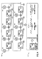
- a keystream 100 is generated using multiple feedback shift registers.
- Each feedback shift register has input, intermediate, and output stages through which data bits are shifted serially in response to a clock signal.
- Data bits 10 from predetermined register stages of multiple feedback shift registers are provided to a first randomization stage 20.
- the output of the first randomization stage 20 is provided to a second randomization stage 30.
- the output of the second randomization stage 30 and data bits 12 from other predetermined register stages of the feedback shift registers are provided to at least one additional randomization stage.
- the data bits are permutated at each randomization stage and the output of a final randomization stage 40 provides the keystream 100.
- the structure of at least one of the feedback shift registers may be varied in response to a polynomial code signal 90 generated by a polynomial code signal generator (e.g., decoding logic unit 80).
- a polynomial code signal generator e.g., decoding logic unit 80
- the polynomial code used to generate the polynomial code signal 90 may be varied.
- the feedback shift registers may comprise a plurality of dynamic feedback shift registers (DFSR) and at least one static feedback shift register (SFSR).
- the two DFSRs may be arranged in parallel.
- the keystream 100 is generated as a nonlinear function of the outputs of both the SFSR and the DFSRs.
- the DSFRs are dynamic shift registers whose structure is varied by the polynomial code signal 90.
- the polynomial code signal 90 may itself be varied in accordance with data bits shifted from a predetermined register stage. It is substantially more difficult to duplicate the keystream 100 if the polynomial code varies.
- the bits that cause the polynomial code 90 to vary are preferably not included in the keystream 100.
- the feedback shift registers may comprise a static feedback shift register A (generally designated 110), a first dynamic feedback shift register B (generally designated 120), and a second dynamic feedback shift register C (generally designated 130).
- Seed data may be input into an input buffer 140.
- the contents of the input buffer 140 may be loaded in parallel into the shift registers 110, 120, and 130 to initialize keystream generation.
- a first portion of the seed data from the input buffer 140 may be provided to the first dynamic feedback shift register B and a second portion of the seed data from the input buffer may be provided to the second dynamic feedback shift register C.
- a third portion of the seed data from the input buffer may be provided to the static feedback shift register A.
- the feedback shift registers 110, 120, and 130 may be constructed using an extended Galois field (GF(2 m )).
- GF Galois field
- a Galois field is a mathematical field extension obtained by considering the coefficients and roots of a given polynomial.
- RGA denotes output from a stage of register A (110)
- RGB denotes output from a stage of register B (120)
- RGC denotes output from a stage of register C (130).
- Figure 2 shows register A having output from L register stages (RGA 0 , RGA 1 , RGA 2 , ... RGA L-1 ).
- the data bits of the feedback shift registers 110, 120, and 130 may be shifted serially from each register stage in response to a clock signal.
- a number of finite field adders may be arranged between predetermined pairs of the register stages of the feedback shift registers 110, 120, and 130, such that one of the inputs to each adder is provided from the preceding register stage and the other input of each adder is fed back from the output terminal of the output stage via a finite field multiplier.
- An example of the structure of each feedback shift register 110, 120, and 130 of Figure 2 is described in detail below in connection with Figures 4, 5, and 6. It is noted that the invention may utilize three or more stages of non-linear functions to combine data bits shifted from predetermined register stages of the feedback shift registers.
- the first randomization stage may comprise one or more randomization tables (e.g., "F1 tables” 150-157) for permuting data bits from predetermined register stages.
- F1 tables 150-157 e.g., "F1 tables" 150-157) for permuting data bits from predetermined register stages.
- F1 tables 150-157 are used.
- the eight F1 tables are shown for purposes of example only, and those skilled in the art will appreciate that the invention can be implemented using any number of F1 tables (or similar non-linear permutation functions) in the first randomization stage.
- the F1 tables 150-157 may be fixed substitution tables used to map data bits shifted from various feedback shift registers to a different value.
- the inputs to each F1 table may be separated by at least one exclusive-or gate in their source feedback shift register structure.
- the data bits from selected register stages of the feedback shift registers may be multiplexed (e.g., at multiplexers 170-173) prior to input into the F1 tables 150-157. Selection by the multiplexers 170-173 between data bits shifted from different predetermined register stages is controlled in response to a data bit shifted from a different predetermined register stage. For example, in Figure 2, two output bits (RGA j and RGA i ) are shifted directly from different stages of register A to multiplexer 170. One of RGA j and RGA i is selected by multiplexer 170 in response to a data bit shifted from register C (RGC k ). Similar operations take place at multiplexers 171, 172, and 173. The output of multiplexers 170, 171, 172, and 173 is provided to F1 tables 150, 153, 154, and 157 respectively.
- F1 table 151 receives input directly from a stage of register A (RGA m ).
- F1 table 152 receives input directly from a stage of register B (RGB p ).
- F1 table 155 receives input directly from a stage of register A (RGA mm ).
- F1 table 156 receives input directly from a stage of register B (RGB pp ).
- the second randomization stage may comprise one or more non-linear mixing functions (e.g., 161, 162) to combine the output of the second randomization stage and data bits from other predetermined register stages of the feedback shift registers.
- non-linear mixing functions 161, 162 are used for purposes of example only.
- the invention can be implemented using any number of non-linear mixing functions (or similar non-linear permutation functions) in the second randomization stage.
- the non-linear logic used by the non-linear mixing functions 161, 162 combines at least 4 tap positions, some of which are from the F1 table outputs, and several others directly from predetermined FSR stages.
- Figure 2 shows non-linear mixing function 161 as having input RGB' i'/j' from F1 table 153, input RGB' p from F1 table 152, input RGA' m from F1 table 151, and input RGA' i/j from F1 table 150, as well as inputs RGA q' and RGB q directly from a stage of register A and a stage of register B respectively.
- ⁇ represents the field element multiplication operation
- ⁇ represents the field element addition operation (bit-wise XOR).
- the third randomization stage (e.g., Final Randomization Stage 40 of Figure 1) may comprise multiple non-linear substitution boxes (S-Boxes) 165.
- the S-Boxes 165 may be 8*8 S-Boxes.
- the third randomization stage may comprise 256 non-linear dynamic 8*8 S-boxes 165 (e.g. , S 0 , S 1 , S 2 , . . .S 255 ).
- a loop counter is provided to count n (number of FSR cycles) to ensure that every element in the dynamic S-Box 165 changes during operation.
- At least one predetermined stage of two of the extended Galois field shift register structures directly provides a randomized byte of S-Box address signals (shown as RGB x and RGA y input into S-Box RAM 166).
- the already highly randomized outputs (g0 and g1) from the non-linear mixing functions 161, 162 are added to the nth element of the S-Box 165, and to the element of S-Box 165 indexed by RGB x /RGA y directly from the FSR structures. This generates highly randomized outputs Y0' and Y1'.
- the S-box elements indexed by n and Y0'/Y1' are then swapped so that every element in (S 0 , S 1 , . . ., S 255 ) is affected during the first 256 cycles of FSR shifting operations.
- the output (pre-keystream 45) from the third randomization stage may be provided to a pre-keystream register 50.
- Alternate bits of the output from said pre-keystream register 50 may be provided to a select chain buffer 70.
- the output from the select chain buffer 70 may be provided to a decoding logic unit 80, which decoding logic unit 80 decodes a particular polynomial for use in generating a polynomial code signal 90, said polynomial code signal 90 being provided to at least one of the dynamic feedback shift registers 120, 130.
- the remaining bits of the output from said pre-keystream register 50 may be provided to a keystream register 60.
- the output of the keystream register 60 provides the keystream 100.
- the pre-keystream 45 may be clocked into the pre-keystream register 50 at the system clock rate. Alternate bytes of the pre-keystream 45 may be clocked at one-half the system clock rate into the select chain buffer 70 by an inverted CLOCK/2 signal. The remaining bytes of the pre-keystream 45 may be clocked at one-half the system clock rate into the keystream register 60 by an uninverted CLOCK/2 signal. This avoids placing contiguous bytes of the pre-keystream 45 into the keystream 100. This also assures that keystream bytes are not used as signals to control selection of the polynomial code signals 90.
- the pre-keystream register 50 is the final output creation stage and produces 8 bits of output data per clock cycle of uninverted CLOCK/2.
- the decoding logic unit 80 uses the bits stored in the select chain buffer 70 to decode a particular polynomial, setting a signal corresponding to a particular polynomial true while setting all other polynomial signals false.
- the decoding logic unit 80 may use a fixed byte substitution table (F2 table 81) to provide up to 2 m different polynomial code signals 90.
- the F2 table 81 may be a fixed substitution table similar to the F1 tables 150-157.
- Certain output of the S-Boxes 165 may be provided to a codestream register 175. This output may be clocked through the codestream register 175 (codestream 48) and added to data bits shifted from at least one of the feedback shift registers 120, 130 via a non-binary adder to produce feedback data bits.
- the feedback data bits may be provided to the input stage and predetermined intermediate stages of at least one of the feedback shift registers 120, 130.
- the codestream 48 is distinct from the pre-keystream 45 and only affects the dynamic FSR structures (120 and 130) and not the static FSR structure (110).
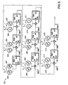
- Figure 3 illustrates a specific configuration of the Figure 2 embodiment of the invention where the polynomials used for the FSRs are constructed over extended Galois Field GF(2 ⁇ 8), and all polynomials are selected to be primitive and irreducible in order to generate a maximum length sequence.
- the degree of these polynomials is 8 so there will be 8 stages of 8-tuple shift register cells used in each FSR. Since the sparseness of the terms for the polynomial can be a source of cryptographic weakness, dense primitive polynomials with many coefficients are used.
- the output from each stage of each FSR may have 8 bits (one byte).
- the three FSRs 110, 120, and 130 require 192 total bits (18 bytes) of information to initialize them. These 192 bits are drawn from 128 bits of input, with half the 128 bits duplicated to provide 192 bits of input to input buffer 140. Input buffer 140 provides 64 bits of input to each FSR 110, 120, and 130.
- a 128 bit (16 byte) input is used to initialize 192 bits (18 bytes) of FSR state.
- the input bytes are numbered from 0 to 15, and are used to initialize the three FSRs A, B, and C.
- Mapping Input to FSRs A, B, and C Input Byte FSR Bytes That Are Initialized Using this Byte FSR Byte FSR Byte FSR Byte 0 B 0 A 0 1 B 1 A 1 2 B 2 A 2 3 B 3 A 3 4 B 4 5 B 5 6 B 6 7 B 7 8 C 0 A 4 9 C 1 A 5 10 C 2 A 6 11 C 3 A 7 12 C 4 13 C 5 14 C 6 15 C 7
- a 128 bit input data seed is stored in the input buffer 140. All of the bits of the input seed are loaded in parallel from the input buffer into dynamic FSR structures B and C. The other third of the input (bytes 0-3 and 8-11) is loaded in parallel into the static FSR structure A.
- input data for each stage should be 64 bits in size (since the actual input size is 128 bits, the above processing step is needed to reduce the information from 192 to 128 bits in size.)
- each pre-keystream byte 45 is generated from a combination of a three-stage non-linear function process.
- certain predetermined data bytes shifted from two separate feedback shift registers (A and B) are permutated by the F1 tables 150-157.
- non-linear functions 161, 162 are used to mix data bytes from different F1 tables as well as data bytes directly from predetermined stages of registers A and B.
- Static FSR structure 110 register A
- two dynamic FSR structures 120 and 130 registers B and C
- Figure 4 Figure 5
- Figure 6 Figure 6
- L 8
- stage 0 the input stage
- stage 7 the output stage
- stage 1 through 6 being the intermediate stages. All the polynomials used in the explanations herein are selected for illustration purposes. It should be appreciated that various other polynomials may be used to implement the invention.
- All the FSRs are constructed over the extended Galois Field, GF (2 ⁇ 8).
- the structure of register A has a fixed, non-dynamic polynomial code and coefficients.
- the polynomial code of the static FSR structure of register A is not varied in response to the polynomial code signal. As shown in Figure 4 the polynomial used for A register is:
- dynamic feedback shift register structures B and C 120 and 130
- data bits are shifted serially in response to a clock signal, and they are also shifted in accordance with a polynomial code signal 90 connected from the output stage into the input stage.
- a number of logic elements are respectively located between predetermined pairs of register stages of registers B and C. The logic elements process a data bit shifted from the preceding stage with the data bit feedback from the output stage, also in accordance with a polynomial code signal 90.
- a polynomial code signal from the decoding logic unit is applied to select one set of polynomial coefficients (i.e. a different set of extended Galois Field multiplier values) from two sets of polynomial coefficients.
- data bits are shifted serially from each stage in response to a clock signal applied to the CLK terminal.
- Data bytes shifted from the register stages are provided respectively at the output terminals RGB 0 through RGB 7 .
- a number of finite field adders 121-127 are respectively located between each pair of register stages.
- One of the inputs to each adder 121-127 is provided from the preceding register stage and the other input to each adder is fed back from output terminal RGB 7 of the eighth output stage via one of two sets of finite field multipliers (e.g., one set includes finite field multipliers 200, 202, 204, 205, 206, 208, 210, 212, and 214; the second set includes 201, 203, 205, 207, 209, 211, 213, and 215). Which set of finite field multipliers is used depends on the polynomial selected in response to the polynomial code 90 (from the decoding logic unit 80 of Figure 3).
- dynamic feedback shift register B shown in Figure 5 uses only two polynomials.
- the least significant bit (lsb) of Decoding Logic Unit 80 output is used to select one of the following polynomials from the dynamic FSR structure B:
- Poly_B1 x ⁇ 8 ⁇ ⁇ 22 ⁇ x ⁇ 7 ⁇ ⁇ 47 ⁇ x ⁇ 6 ⁇ 0 ⁇ x ⁇ 5 ⁇ ⁇ 230 ⁇ x ⁇ 4 ⁇ ⁇ 94 ⁇ x ⁇ 3 ⁇ ⁇ 202 ⁇ x ⁇ 2 ⁇ ⁇ 28 ⁇ x ⁇ ⁇ 188.
- dynamic feedback shift register C (130) is shown in Figure 6.
- the function of register C corresponds to that of register B shown in Figure 5, with finite field adders 221-227 of register C equivalent to the finite field adders 121-127 of register B of Figure 5 and finite field multipliers 230-245 of register C equivalent to finite field multipliers 200-215 of register B of Figure 5.
- Poly_C1 x ⁇ 8 ⁇ ⁇ 39 ⁇ x ⁇ 7 ⁇ ⁇ 203 ⁇ x ⁇ 6 ⁇ 0 ⁇ x ⁇ 5 ⁇ ⁇ 185 ⁇ x ⁇ 4 ⁇ ⁇ 151 ⁇ x ⁇ 3 ⁇ ⁇ 114 ⁇ x ⁇ 2 ⁇ ⁇ 7 ⁇ x ⁇ ⁇ 47.
- the polynomial code signal 90 that is applied in the dynamic FSRs 120 and 130 varies in accordance with data bits shifted from a predetermined register stage.
- An F2 table 81 is used in the Decoding Logic Unit (DLU) 80 to generate the polynomial code signal.
- DLU Decoding Logic Unit
- the decoding logic unit 80 of Figure 3 uses the least significant bit (lsb) of F2 table output to select one of two polynomials from the dynamic FSRs 120, 130.
- Lsb least significant bit
- 2 different polynomials are used in the B-register structure and C-register structure, and one polynomial is used in the A-register structure. Therefore, only one bit in every other pre-keystream byte after F2 table substitution is used directly to select between the two polynomials, POLY_AO(POLY_BO) and POLY_A1(POLY_B1).
- Alternate bytes (8 bits) from the pre-keystream 45 are processed to vary the polynomial code signal 90, and the remaining bytes of the pre-keystream 45 are processed to provide the keystream 100.
- the bytes that cause the polynomial code signal 90 to be varied are not included in the keystream 100.
- the multiplexers 170-173 use the output from predetermined register stages of register C to select between data bytes shifted from different predetermined register stages of registers A and B to provide some of the inputs to the F1 tables (e.g., F1 tables 150, 153, 154, and 157).
- Each multiplexer 170-173 is a 2:1 multiplexer. For example, two output bits (RGA 0 and RGA 7 ) are shifted directly from different stages of register A to multiplexer 170. One of RGA 0 and RGA 7 is selected by multiplexer 170 in response to a data bit shifted from register C (RGC 6 ). Similar operations take place at multiplexers 171, 172, and 173. The output of multiplexers 170, 171, 172, and 173 is provided to F1 tables 150, 153, 154, and 157 respectively.
- MUX 170 and 172 Detailed multiplexer settings for multiplexers (MUX) 170 and 172 are shown in the table below.
- Multiplexers may also be used to provide the address signal to the S-Box substitution function 165.
- the inverse of MUX 170 (MUX 170 -1 ) is used to select alternate bits from RGA 0 and RGA 7 .
- MUX 173 -1 The inverse of MUX 173 (MUX 173 -1 ) is used to select alternate bits from RGB 0 and RGB 7 .
- Two of eight register outputs from each shift register are tapped as direct inputs to the F1 tables 151, 152, 155, 156. No tap is used more than once.
- Input to the remaining F1 tables 150, 153, 154, and 157 are from the multiplexers 170, 171, 172, and 173 respectively.
- 6 ⁇ RGA 2 ⁇ RGB' 4 ⁇ RGA' 5 ⁇ RGB 3 g1 RGA' 1
- 7 is a field element constructed from selecting 8 bits from RGA 0 and RGA 7 based on RGC 6 , and then passing the selected bits to the F1 table 150.
- 6 is a field element constructed from selecting 8 bits from RGB 1 and RGB 6 based on RGC 0 , and then passing the selected bits to the F1 table 153.
- 6 is a field element constructed from selecting 8 bits from RGA 1 and RGA 6 based on RGC 6 , and then passing the selected bits to the F1 table 172.
- 7 is a field element constructed from selecting 8 bits from RGB 0 and RGB 7 based on RGC 0 , and then passing the selected bits to the F1 table 157.
- the 8 * 8 S-Box 165 is used to provide individual pre-keystream bytes 45 and codestream bytes 48 respectively from output terminal Y1 and Y0 in accordance with the contents of the output from the non-linear mix functions 161, 162 and two bytes of data from the A and B register structures.
- the entries of the S-Box are a permutation of the numbers 0 through 255, and the address of the S-Box is a function of loop counter n, g0, g1, RGB 0
- the S-box permutation process can be formulated in accordance with the following relationships: n from 0 to runup_Cycles
- the Codestream Register 175 receives codestream bits 48 from the Y1 output terminal of the S-Box 165 in response to the address signal from the A and B structures, and also from the non-linear mix functions 161, 162.
- the codestream bytes 48 are clocked through the Codestream Register 175, and added by a non-binary adder (XOR) to the data bytes (RGB 7 , RGC 7 ) shifted from the MSB output stage (stage 7) of register B and register C. This process provides a feedback data byte, which is then fed back both to the input stage (stage 0) and to predetermined intermediate stages of registers B and C in accordance with the applied polynomial code 90.
- XOR non-binary adder
- Keystream bytes 100 from the Keystream Register 60 are produced based on the control clock, CLOCK. These bytes are assembled to form the 7 bytes or 56 bits of output only after the algorithm has had adequate mixing time to circulate data among the FSRs.
- the amount of mixing time is measured in the number of clock cycles of CLOCK between the time FSRs A, B, and C are initialized, and the time that the Keystream Register 60 byte output is stored.
- the present invention provides improved methods and apparatus for generating a cryptographically robust keystream for use in data encryption and decryption.
Claims (46)
- Ein Verfahren zum Erzeugen einer Schlüsselzeichenfolge, das die folgenden Schritte beinhaltet:einer ersten Randomisierungsphase (150-157) Datenbits aus vorbestimmten Registerphasen mehrfacher rückgekoppelter Schieberegister (110, 120, 130) bereitstellen, wobei jedes rückgekoppelte Schieberegister Eingabe-, Zwischen- und Ausgabephasen aufweist, durch die die Datenbits seriell als Reaktion auf ein Taktsignal verschoben werden; gekennzeichnet durch die folgenden zusätzlichen Schritte:einer zweiten Randomisierungsphase (161) die Ausgabe der ersten Randomisierungsphase bereitstellen;der mindestens einen zusätzlichen Randomisierungsphase (165) die Ausgabe der zweiten Randomisierungsphase und die Datenbits aus anderen vorbestimmten Registerphasen der rückgekoppelten Schieberegister bereitstellen, wobeidie Datenbits in jeder Randomisierungsphase permutiert werden und die Ausgabe einer endgültigen Randomisierungsphase die Schlüsselzeichenfolge bereitstellt.
- Verfahren gemäß Anspruch 1, wobei eine dritte Randomisierungsphase die endgültige Randomisierungsphase ist.
- Verfahren gemäß Anspruch 1 oder 2, das ferner die folgenden Schritte beinhaltet:Variieren von mindestens einer rückgekoppelten Schieberegisterstruktur als Reaktion auf ein durch einen Polynomcodesignalgenerator erzeugtes Polynomcodesignal.
- Verfahren gemäß Anspruch 3, das ferner den folgenden Schritt beinhaltet:Variieren des Polynomcodes, der zum Erzeugen des Polynomcodesignals verwendet wird.
- Verfahren gemäß einem der Ansprüche 1 bis 4, wobei die rückgekoppelten Schieberegister Folgendes beinhalten:eine Vielzahl dynamischer rückgekoppelter Schieberegister undmindestens ein statisches rückgekoppeltes Schieberegister.
- Verfahren gemäß einem der Ansprüche 1 bis 4, wobei die rückgekoppelten Schieberegister Folgendes beinhalten:ein erstes dynamisches rückgekoppeltes Schieberegister,ein zweites dynamisches rückgekoppeltes Schieberegister, undein statisches rückgekoppeltes Schieberegister.
- Verfahren gemäß Anspruch 6, das ferner die folgenden Schritte beinhaltet:Startparameter-Daten in einen Eingabepuffer eingeben;dem ersten dynamischen rückgekoppelten Schieberegister einen ersten Abschnitt der Startparameter-Daten des Eingabepuffers bereitstellen;dem zweiten dynamischen rückgekoppelten Schieberegister einen zweiten Abschnitt der Startparameter-Daten des Eingabepuffers bereitstellen, unddem statischen rückgekoppelten Schieberegister einen dritten Abschnitt der Startparameter-Daten des Eingabepuffers bereitstellen.
- Verfahren gemäß Anspruch 7, wobei:die Datenbits des dynamischen rückgekoppelten Schieberegisters seriell von jeder Registerphase als Reaktion auf ein Taktsignal verschoben werden;eine Anzahl von endlichen Feldaddierern zwischen vorbestimmten Paaren der Registerphasen der dynamischen rückgekoppelten Schieberegister angeordnet werden, so dass eine der Eingaben in jeden Addierer von der vorangehenden Registerphase bereitgestellt wird und die andere Eingabe von jedem Addierer von dem Ausgabeterminal der Ausgabephase über einen endlichen Feldmultiplikator bereitgestellt wird.
- Verfahren gemäß einem der Ansprüche 1 bis 8, wobei die erste Randomisierungsphase eine Randomisierungstabelle zum Permutieren von Datenbits aus vorbestimmten Registerphasen beinhaltet.
- Verfahren gemäß einem der Ansprüche 1 bis 9, wobei die zweite Randomisierungsphase eine nichtlineare Mischfunktion beinhaltet, um die Ausgabe der zweiten Randomisierungsphase und Datenbits aus anderen vorbestimmten Registerphasen der rückgekoppelten Schieberegister zu kombinieren.
- Verfahren gemäß einem der Ansprüche 1 bis 10, wobei die endgültige Randomisierungsphase 256 nichtlineare 8*8 S-Boxen beinhaltet.
- Verfahren gemäß einem der Ansprüche 1 bis 11, wobei die rückgekoppelten Schieberegister unter Verwendung eines erweiterten Galoisfelds GF (2m) konstruiert werden.
- Verfahren gemäß Anspruch 12, wobei m gleich acht ist.
- Verfahren gemäß Anspruch 12 oder 13, wobei die für die rückgekoppelten Schieberegister verwendeten Polynome primitiv und irreduzibel sind.
- Verfahren gemäß einem der Ansprüche 1 bis 14, wobei die erste Randomisierungsphase mehrfache Randomisierungstabellen zum Permutieren von Datenbits aus vorbestimmten Registerphasen beinhaltet.
- Verfahren gemäß Anspruch 15, wobei die mehrfachen Randomisierungstabellen acht Randomisierungstabellen beinhalten.
- Verfahren gemäß einem der Ansprüche 1 bis 16, das ferner folgenden Schritt beinhaltet:die Datenbits aus den rückgekoppelten Schieberegistern vor der Eingabe in die erste Randomisierungsphase multiplexieren.
- Verfahren gemäß einem der Ansprüche 1 bis 17, das ferner die folgenden Schritte beinhaltet:einem Vor-Schlüsselzeichenfolge-Register die Ausgabe aus der endgültigen Randomisierungsphase bereitstellen;einem ausgewählten Kettenpuffer alternierende Bits der Ausgabe aus dem Vor-Schlüsselzeichenfolge-Register bereitstellen;einem decodierenden Logikbaustein die Ausgabe des ausgewählten Kettenpuffers bereitstellen, wobei der decodierende Logikbaustein ein bestimmtes Polynom zur Verwendung beim Erzeugen eines Polynomcodesignals decodiert, wobei mindestens einem rückgekoppelten Schieberegister das Polynomcodesignal bereitgestellt wird; undeinem Schlüsselzeichenfolge-Register die verbleibenden Bits der Ausgabe aus dem Vor-Schlüsselzeichenfolge-Register bereitstellen, wobei die Ausgabe des Schlüsselzeichenfolge-Registers das Schlüsselzeichen bereitstellt.
- Verfahren gemäß einem der Ansprüche 1 bis 18, wobei die endgültige Randomisierungsphase mehrere nichtlineare S-Boxen beinhaltet.
- Verfahren gemäß Anspruch 19, wobei die S-Boxen 8*8 S-Boxen sind.
- Verfahren gemäß Anspruch 19, das ferner die folgenden Schritte beinhaltet:einem Codestrom-Register eine gewisse Ausgabe der S-Boxen bereitstellen;die Ausgabe durch das Codestrom-Register takten;die Ausgabe an von mindestens einem der rückgekoppelten Schieberegister über einen nichtbinären Addierer verschobenen Datenbits zugeben, um rückgekoppelte Datenbits zu produzieren;der Eingabephase und den vorbestimmten Zwischenphasen von mindestens einem der rückgekoppelten Schieberegister die rückgekoppelten Datenbits bereitstellen.
- Verfahren gemäß einem der Ansprüche 1 bis 21, wobei:den mehreren rückgekoppelten Schieberegistern ein 192 Bit geteilter Startparameter-Schlüssel bereitgestellt wird; undeine 56 Bit Schlüsselzeichenfolge erzeugt wird.
- Verfahren gemäß Anspruch 22, wobei der 192 Bit geteilte Startparameter-Schlüssel durch das Duplizieren der Hälfte der Bits aus einer 128 Bit Eingabe gewonnen wird.
- Eine Schlüsselzeichenfolgegeneratorvorrichtung, die Folgendes beinhaltet:mehrere rückgekoppelte Schieberegister (110, 120, 130), wobei jedes rückgekoppelte Schieberegister Eingabe-, Zwischen- und Ausgabephasen aufweist, durch die Datenbits seriell als Reaktion auf ein Taktsignal verschoben werden, gekennzeichnet durcheine erste Randomisierungsphase (150-157), die die Ausgabe von vorbestimmten Registerphasen der mehrfachen rückgekoppelten Schieberegister empfängt;eine zweite Randomisierungsphase (161), die die Ausgabe von der ersten Randomisierungsphase empfängt;eine dritte Randomisierungsphase (165), die die Ausgabe von der zweiten Randomisierungsphase und Datenbits von anderen vorbestimmten Registerphasen der rückgekoppelten Schieberegister empfängt, wobeidie Datenbits in jeder Randomisierungsphase permutiert werden und die Ausgabe einer endgültigen Randomisierungsphase die Schlüsselzeichenfolge bereitstellt.
- Vorrichtung gemäß Anspruch 24, wobei die dritte Randomisierungsphase die endgültige Randomisierungsphase ist.
- Vorrichtung gemäß Anspruch 24 oder 25, wobei:mindestens eine rückgekoppelte Schieberegisterstruktur als Reaktion auf ein durch einen Polynomcodesignalgenerator erzeugtes Polynomcodesignal variiert wird.
- Vorrichtung gemäß Anspruch 26, wobei:der Polynomcode, der zum Erzeugen des Polynomcodesignals verwendet wird, variiert wird.
- Vorrichtung gemäß einem der Ansprüche 24 bis 27, wobei die rückgekoppelten Schieberegister Folgendes beinhalten:eine Vielzahl dynamischer rückgekoppelter Schieberegister, undmindestens ein statisches rückgekoppeltes Schieberegister.
- Vorrichtung gemäß einem der Ansprüche 24 bis 28, wobei die rückgekoppelten Schieberegister Folgendes beinhalten:ein erstes dynamisches rückgekoppeltes Schieberegister;ein zweites dynamisches rückgekoppeltes Schieberegister, undein statisches rückgekoppeltes Schieberegister.
- Vorrichtung gemäß Anspruch 29, wobei:Startparameter-Daten in einen Eingabepuffer eingegeben werden;dem ersten dynamischen rückgekoppelten Schieberegister ein erster Abschnitt der Startparameter-Daten aus dem Eingabepuffer bereitgestellt wird,dem zweiten dynamischen rückgekoppelten Schieberegister ein zweiter Abschnitt der Startparameter-Daten aus dem Eingabepuffer bereitgestellt wird, unddem statischen rückgekoppelten Schieberegister ein dritter Abschnitt der Startparameter-Daten aus dem Eingabepuffer bereitgestellt wird.
- Vorrichtung gemäß Anspruch 30, wobei:die Datenbits des dynamischen rückgekoppelten Schieberegisters seriell von jeder Registerphase als Reaktion auf ein Taktsignal verschoben werden;eine Anzahl von endlichen Feldaddierern zwischen vorbestimmten Paaren der Registerphasen der dynamischen rückgekoppelten Schieberegister angeordnet werden, so dass eine der Eingaben in jeden Addierer von der vorangehenden Registerphase bereitgestellt wird und die andere Eingabe von jedem Addierer von dem Ausgabeterminal der Ausgabephase über einen endlichen Feldmultiplikator bereitgestellt wird.
- Vorrichtung gemäß einem der Ansprüche 24 bis 31, wobei die erste Randomisierungsphase eine Randomisierungstabelle zum Permutieren von Datenbits aus vorbestimmten Registerphasen beinhaltet.
- Vorrichtung gemäß einem der Ansprüche 24 bis 32, wobei die zweite Randomisierungsphase eine nichtlineare Mischfunktion beinhaltet, um die Ausgabe der zweiten Randomisierungsphase und Datenbits aus anderen vorbestimmten Registerphasen der rückgekoppelten Schieberegister zu kombinieren.
- Vorrichtung gemäß einem der Ansprüche 24 bis 33, wobei die dritte Randomisierungsphase mehrere nichtlineare S-Boxen beinhaltet.
- Vorrichtung gemäß Anspruch 34, wobei die S-Boxen 8*8 S-Boxen sind.
- Vorrichtung gemäß einem der Ansprüche 24 bis 35, wobei die dritte Randomisierungsphase 256 nichtlineare 8*8 S-Boxen beinhaltet.
- Vorrichtung gemäß einem der Ansprüche 24 bis 36, wobei die rückgekoppelten Schieberegister unter Verwendung eines erweiterten Galoisfelds GF (2m) konstruiert werden.
- Vorrichtung gemäß Anspruch 37, wobei m gleich acht ist.
- Vorrichtung gemäß Anspruch 37 oder 38, wobei die für die rückgekoppelten Schieberegister verwendeten Polynome primitiv und irreduzibel sind.
- Vorrichtung gemäß einem der Ansprüche 24 bis 39, wobei die erste Randomisierungsphase mehrere Randomisierungstabellen zum Permutieren von Datenbits aus vorbestimmten Registerphasen beinhaltet.
- Vorrichtung gemäß Anspruch 40, wobei die mehrfachen Randomisierungstabellen acht Randomisierungstabellen beinhalten.
- Vorrichtung gemäß einem der Ansprüche 24 bis 41, wobei:die Datenbits aus den rückgekoppelten Schieberegistern vor derEingabe in die erste Randomisierungsphase gemultiplext werden.
- Vorrichtung gemäß einem der Ansprüche 24 bis 42, die ferner Folgendes beinhaltet:ein Vor-Schlüsselzeichenfolge-Register zum Empfangen der Ausgabe aus der dritten Randomisierungsphase;einen ausgewählten Kettenpuffer zum Empfangen von alternierenden Bits der Ausgabe aus dem Vor-Schlüsselzeichenfolge-Register;einen decodierenden Logikbaustein zum Empfangen der Ausgabe aus dem ausgewählten Kettenpuffer, wobei der decodierende Logikbaustein ein bestimmtes Polynom zur Verwendung beim Erzeugen eines Polynomcodesignals decodiert, wobei mindestens einem rückgekoppelten Schieberegister das Polynomcodesignal bereitgestellt wird; undein Schlüsselzeichenfolge-Register zum Empfangen der verbleibenden Bits der Ausgabe aus dem Vor-Schlüsselzeichenfolge-Register, wobei die Ausgabe des Schlüsselzeichenfolge-Registers das Schlüsselzeichen bereitstellt.
- Vorrichtung gemäß Anspruch 43, wobei:die dritte Randomisierungsphase mehrere nichtlineare S-Boxen beinhaltet;eine gewisse Ausgabe der S-Boxen an ein Codestrom-Register bereitgestellt wird;die Ausgabe durch das Codestrom-Register getaktet wird;die Ausgabe an von mindestens einem der rückgekoppelten Schieberegister über einen nichtbinären Addierer verschobenen Datenbits zugegeben wird, um rückgekopplte Datenbits zu produzieren; undder Eingabephase und den vorbestimmten Zwischenphasen von mindestens einem der rückgekoppelten Schieberegister die Rückkopplungsdatenbits bereitgestellt werden.
- Vorrichtung gemäß einem der Ansprüche 24 bis 44, wobei:den mehreren rückgekoppelten Schieberegistern ein 192 Bit geteilter Startparameter-Schlüssel bereitgestellt wird; undeine 56 Bit Schlüsselzeichenfolge erzeugt wird.
- Vorrichtung gemäß Anspruch 45, wobei der 192 Bit geteilte Startparameter-Schlüssel durch das Duplizieren der Hälfte der Bits aus einer 128 Bit Eingabe gewonnen wird.
Applications Claiming Priority (3)
| Application Number | Priority Date | Filing Date | Title |
|---|---|---|---|
| US16718599P | 1999-11-23 | 1999-11-23 | |
| US167185P | 1999-11-23 | ||
| PCT/US2000/031539 WO2001039417A2 (en) | 1999-11-23 | 2000-11-17 | Methods and apparatus for keystream generation |
Publications (2)
| Publication Number | Publication Date |
|---|---|
| EP1232603A2 EP1232603A2 (de) | 2002-08-21 |
| EP1232603B1 true EP1232603B1 (de) | 2005-11-09 |
Family
ID=22606308
Family Applications (1)
| Application Number | Title | Priority Date | Filing Date |
|---|---|---|---|
| EP00980446A Expired - Lifetime EP1232603B1 (de) | 1999-11-23 | 2000-11-17 | Verfahren und vorrichtungen zur erzeugung einer schlüsselsequenz |
Country Status (9)
| Country | Link |
|---|---|
| EP (1) | EP1232603B1 (de) |
| KR (1) | KR100756435B1 (de) |
| CN (1) | CN1425230A (de) |
| AT (1) | ATE309654T1 (de) |
| AU (1) | AU1770501A (de) |
| CA (1) | CA2391997C (de) |
| DE (1) | DE60023934T2 (de) |
| TW (1) | TW548937B (de) |
| WO (1) | WO2001039417A2 (de) |
Cited By (1)
| Publication number | Priority date | Publication date | Assignee | Title |
|---|---|---|---|---|
| CN103701591B (zh) * | 2013-12-23 | 2016-08-31 | 中国科学院数学与系统科学研究院 | 一种序列密码实现方法和密钥流生成方法及装置 |
Families Citing this family (4)
| Publication number | Priority date | Publication date | Assignee | Title |
|---|---|---|---|---|
| US7822797B2 (en) | 2002-07-29 | 2010-10-26 | Broadcom Corporation | System and method for generating initial vectors |
| KR100584604B1 (ko) * | 2004-08-14 | 2006-05-30 | 삼성전자주식회사 | 디바이스를 인증하기 위한 키 생성 방법/장치 및 디바이스인증 방법/장치 |
| CN100459493C (zh) * | 2005-12-29 | 2009-02-04 | 北京浦奥得数码技术有限公司 | 流密码生成器、随机数生成方法、加密系统及加密方法 |
| US10025956B2 (en) | 2015-12-18 | 2018-07-17 | Intel Corporation | Techniques to compress cryptographic metadata for memory encryption |
Family Cites Families (5)
| Publication number | Priority date | Publication date | Assignee | Title |
|---|---|---|---|---|
| US4860353A (en) * | 1988-05-17 | 1989-08-22 | General Instrument Corporation | Dynamic feedback arrangement scrambling technique keystream generator |
| KR0153962B1 (ko) * | 1994-10-31 | 1998-12-01 | 배순훈 | 피드백 시프트 레지스터 |
| US5701136A (en) * | 1995-03-06 | 1997-12-23 | Thomson Consumer Electronics S.A. | Liquid crystal display driver with threshold voltage drift compensation |
| KR970049468A (ko) * | 1995-12-30 | 1997-07-29 | 김주용 | 난수 발생 장치 |
| JPH1056361A (ja) * | 1996-08-07 | 1998-02-24 | Matsushita Electric Ind Co Ltd | 疑似雑音系列発生器 |
-
2000
- 2000-11-17 KR KR1020027006549A patent/KR100756435B1/ko active IP Right Grant
- 2000-11-17 AT AT00980446T patent/ATE309654T1/de not_active IP Right Cessation
- 2000-11-17 EP EP00980446A patent/EP1232603B1/de not_active Expired - Lifetime
- 2000-11-17 AU AU17705/01A patent/AU1770501A/en not_active Abandoned
- 2000-11-17 DE DE60023934T patent/DE60023934T2/de not_active Expired - Fee Related
- 2000-11-17 WO PCT/US2000/031539 patent/WO2001039417A2/en active IP Right Grant
- 2000-11-17 CN CN00818544.1A patent/CN1425230A/zh active Pending
- 2000-11-17 CA CA002391997A patent/CA2391997C/en not_active Expired - Lifetime
- 2000-11-23 TW TW089124901A patent/TW548937B/zh not_active IP Right Cessation
Cited By (1)
| Publication number | Priority date | Publication date | Assignee | Title |
|---|---|---|---|---|
| CN103701591B (zh) * | 2013-12-23 | 2016-08-31 | 中国科学院数学与系统科学研究院 | 一种序列密码实现方法和密钥流生成方法及装置 |
Also Published As
| Publication number | Publication date |
|---|---|
| KR100756435B1 (ko) | 2007-09-07 |
| WO2001039417A3 (en) | 2002-01-17 |
| TW548937B (en) | 2003-08-21 |
| ATE309654T1 (de) | 2005-11-15 |
| DE60023934D1 (de) | 2005-12-15 |
| EP1232603A2 (de) | 2002-08-21 |
| DE60023934T2 (de) | 2006-08-10 |
| KR20020060237A (ko) | 2002-07-16 |
| CA2391997C (en) | 2007-07-24 |
| CN1425230A (zh) | 2003-06-18 |
| WO2001039417A2 (en) | 2001-05-31 |
| AU1770501A (en) | 2001-06-04 |
| CA2391997A1 (en) | 2001-05-31 |
Similar Documents
| Publication | Publication Date | Title |
|---|---|---|
| US6314187B1 (en) | Method for encryption or decryption using finite group operations | |
| US7295671B2 (en) | Advanced encryption standard (AES) hardware cryptographic engine | |
| US10320554B1 (en) | Differential power analysis resistant encryption and decryption functions | |
| JP4828068B2 (ja) | コンピュータで効率的な線形フィードバック・シフト・レジスタ | |
| US5297207A (en) | Machine generation of cryptographic keys by non-linear processes similar to processes normally associated with encryption of data | |
| US6295606B1 (en) | Method and apparatus for preventing information leakage attacks on a microelectronic assembly | |
| AU767265B2 (en) | Robust random number generator | |
| US6804354B1 (en) | Cryptographic isolator using multiplication | |
| US11689353B2 (en) | Tweakable block ciphers for secure data encryption | |
| US20070294531A1 (en) | System and methods for a vernam stream cipher, a keyed one-way hash and a non-cyclic pseudo-random number generator | |
| JPS5873257A (ja) | 暗号化装置 | |
| EP1038370B1 (de) | Synchrone bitstromverschlüsselung | |
| JPH08505275A (ja) | 暗号ストリームを発生させるための装置及び方法 | |
| US20030053625A1 (en) | Self-synchronizing, stream-oriented data encryption technique | |
| US6961427B1 (en) | Methods and apparatus for keystream generation | |
| JP2009116348A (ja) | データの非相関化方法 | |
| US6931127B2 (en) | Encryption device using data encryption standard algorithm | |
| EP1232603B1 (de) | Verfahren und vorrichtungen zur erzeugung einer schlüsselsequenz | |
| JP4470135B2 (ja) | 擬似乱数生成システム | |
| JP2006517036A (ja) | マスクされたデータを操作する装置及び方法 | |
| US5859912A (en) | Digital information privacy system | |
| KR100416971B1 (ko) | 암호시스템에 사용하기 위한 랜덤 키스트림 생성 장치 및방법 | |
| AU750408B2 (en) | A method of combining a serial keystream output with binary information | |
| WO2004045134A1 (en) | Self-synchronizing, stream-oriented data encryption technique | |
| RU2184423C2 (ru) | Способ блочного итеративного шифрования цифровых данных |
Legal Events
| Date | Code | Title | Description |
|---|---|---|---|
| PUAI | Public reference made under article 153(3) epc to a published international application that has entered the european phase |
Free format text: ORIGINAL CODE: 0009012 |
|
| 17P | Request for examination filed |
Effective date: 20020531 |
|
| AK | Designated contracting states |
Kind code of ref document: A2 Designated state(s): AT BE CH CY DE DK ES FI FR GB GR IE IT LI LU MC NL PT SE TR |
|
| AX | Request for extension of the european patent |
Free format text: AL;LT;LV;MK;RO;SI |
|
| GRAP | Despatch of communication of intention to grant a patent |
Free format text: ORIGINAL CODE: EPIDOSNIGR1 |
|
| GRAS | Grant fee paid |
Free format text: ORIGINAL CODE: EPIDOSNIGR3 |
|
| GRAA | (expected) grant |
Free format text: ORIGINAL CODE: 0009210 |
|
| AK | Designated contracting states |
Kind code of ref document: B1 Designated state(s): AT BE CH CY DE DK ES FI FR GB GR IE IT LI LU MC NL PT SE TR |
|
| PG25 | Lapsed in a contracting state [announced via postgrant information from national office to epo] |
Ref country code: IT Free format text: LAPSE BECAUSE OF FAILURE TO SUBMIT A TRANSLATION OF THE DESCRIPTION OR TO PAY THE FEE WITHIN THE PRESCRIBED TIME-LIMIT;WARNING: LAPSES OF ITALIAN PATENTS WITH EFFECTIVE DATE BEFORE 2007 MAY HAVE OCCURRED AT ANY TIME BEFORE 2007. THE CORRECT EFFECTIVE DATE MAY BE DIFFERENT FROM THE ONE RECORDED. Effective date: 20051109 Ref country code: NL Free format text: LAPSE BECAUSE OF FAILURE TO SUBMIT A TRANSLATION OF THE DESCRIPTION OR TO PAY THE FEE WITHIN THE PRESCRIBED TIME-LIMIT Effective date: 20051109 Ref country code: LI Free format text: LAPSE BECAUSE OF FAILURE TO SUBMIT A TRANSLATION OF THE DESCRIPTION OR TO PAY THE FEE WITHIN THE PRESCRIBED TIME-LIMIT Effective date: 20051109 Ref country code: TR Free format text: LAPSE BECAUSE OF FAILURE TO SUBMIT A TRANSLATION OF THE DESCRIPTION OR TO PAY THE FEE WITHIN THE PRESCRIBED TIME-LIMIT Effective date: 20051109 Ref country code: CH Free format text: LAPSE BECAUSE OF FAILURE TO SUBMIT A TRANSLATION OF THE DESCRIPTION OR TO PAY THE FEE WITHIN THE PRESCRIBED TIME-LIMIT Effective date: 20051109 Ref country code: AT Free format text: LAPSE BECAUSE OF FAILURE TO SUBMIT A TRANSLATION OF THE DESCRIPTION OR TO PAY THE FEE WITHIN THE PRESCRIBED TIME-LIMIT Effective date: 20051109 Ref country code: BE Free format text: LAPSE BECAUSE OF FAILURE TO SUBMIT A TRANSLATION OF THE DESCRIPTION OR TO PAY THE FEE WITHIN THE PRESCRIBED TIME-LIMIT Effective date: 20051109 Ref country code: FI Free format text: LAPSE BECAUSE OF FAILURE TO SUBMIT A TRANSLATION OF THE DESCRIPTION OR TO PAY THE FEE WITHIN THE PRESCRIBED TIME-LIMIT Effective date: 20051109 |
|
| REG | Reference to a national code |
Ref country code: GB Ref legal event code: FG4D |
|
| REG | Reference to a national code |
Ref country code: CH Ref legal event code: EP |
|
| PG25 | Lapsed in a contracting state [announced via postgrant information from national office to epo] |
Ref country code: CY Free format text: LAPSE BECAUSE OF FAILURE TO SUBMIT A TRANSLATION OF THE DESCRIPTION OR TO PAY THE FEE WITHIN THE PRESCRIBED TIME-LIMIT Effective date: 20051117 Ref country code: IE Free format text: LAPSE BECAUSE OF NON-PAYMENT OF DUE FEES Effective date: 20051117 |
|
| PGFP | Annual fee paid to national office [announced via postgrant information from national office to epo] |
Ref country code: FR Payment date: 20051118 Year of fee payment: 6 |
|
| PG25 | Lapsed in a contracting state [announced via postgrant information from national office to epo] |
Ref country code: MC Free format text: LAPSE BECAUSE OF NON-PAYMENT OF DUE FEES Effective date: 20051130 |
|
| PGFP | Annual fee paid to national office [announced via postgrant information from national office to epo] |
Ref country code: DE Payment date: 20051130 Year of fee payment: 6 |
|
| PGFP | Annual fee paid to national office [announced via postgrant information from national office to epo] |
Ref country code: GB Payment date: 20051209 Year of fee payment: 6 |
|
| REG | Reference to a national code |
Ref country code: IE Ref legal event code: FG4D |
|
| REF | Corresponds to: |
Ref document number: 60023934 Country of ref document: DE Date of ref document: 20051215 Kind code of ref document: P |
|
| PG25 | Lapsed in a contracting state [announced via postgrant information from national office to epo] |
Ref country code: LU Free format text: LAPSE BECAUSE OF NON-PAYMENT OF DUE FEES Effective date: 20060109 |
|
| PG25 | Lapsed in a contracting state [announced via postgrant information from national office to epo] |
Ref country code: DK Free format text: LAPSE BECAUSE OF FAILURE TO SUBMIT A TRANSLATION OF THE DESCRIPTION OR TO PAY THE FEE WITHIN THE PRESCRIBED TIME-LIMIT Effective date: 20060209 Ref country code: SE Free format text: LAPSE BECAUSE OF FAILURE TO SUBMIT A TRANSLATION OF THE DESCRIPTION OR TO PAY THE FEE WITHIN THE PRESCRIBED TIME-LIMIT Effective date: 20060209 Ref country code: GR Free format text: LAPSE BECAUSE OF FAILURE TO SUBMIT A TRANSLATION OF THE DESCRIPTION OR TO PAY THE FEE WITHIN THE PRESCRIBED TIME-LIMIT Effective date: 20060209 |
|
| PG25 | Lapsed in a contracting state [announced via postgrant information from national office to epo] |
Ref country code: ES Free format text: LAPSE BECAUSE OF FAILURE TO SUBMIT A TRANSLATION OF THE DESCRIPTION OR TO PAY THE FEE WITHIN THE PRESCRIBED TIME-LIMIT Effective date: 20060220 |
|
| PG25 | Lapsed in a contracting state [announced via postgrant information from national office to epo] |
Ref country code: PT Free format text: LAPSE BECAUSE OF FAILURE TO SUBMIT A TRANSLATION OF THE DESCRIPTION OR TO PAY THE FEE WITHIN THE PRESCRIBED TIME-LIMIT Effective date: 20060410 |
|
| NLV1 | Nl: lapsed or annulled due to failure to fulfill the requirements of art. 29p and 29m of the patents act | ||
| REG | Reference to a national code |
Ref country code: CH Ref legal event code: PL |
|
| ET | Fr: translation filed | ||
| REG | Reference to a national code |
Ref country code: IE Ref legal event code: MM4A |
|
| PLBE | No opposition filed within time limit |
Free format text: ORIGINAL CODE: 0009261 |
|
| STAA | Information on the status of an ep patent application or granted ep patent |
Free format text: STATUS: NO OPPOSITION FILED WITHIN TIME LIMIT |
|
| 26N | No opposition filed |
Effective date: 20060810 |
|
| PG25 | Lapsed in a contracting state [announced via postgrant information from national office to epo] |
Ref country code: DE Free format text: LAPSE BECAUSE OF NON-PAYMENT OF DUE FEES Effective date: 20070601 |
|
| GBPC | Gb: european patent ceased through non-payment of renewal fee |
Effective date: 20061117 |
|
| REG | Reference to a national code |
Ref country code: FR Ref legal event code: ST Effective date: 20070731 |
|
| PG25 | Lapsed in a contracting state [announced via postgrant information from national office to epo] |
Ref country code: GB Free format text: LAPSE BECAUSE OF NON-PAYMENT OF DUE FEES Effective date: 20061117 |
|
| PG25 | Lapsed in a contracting state [announced via postgrant information from national office to epo] |
Ref country code: FR Free format text: LAPSE BECAUSE OF NON-PAYMENT OF DUE FEES Effective date: 20061130 |
|
| P01 | Opt-out of the competence of the unified patent court (upc) registered |
Effective date: 20230516 |