EP1231647A1 - Reference data coding in solid state image sensors - Google Patents
Reference data coding in solid state image sensors Download PDFInfo
- Publication number
- EP1231647A1 EP1231647A1 EP01301123A EP01301123A EP1231647A1 EP 1231647 A1 EP1231647 A1 EP 1231647A1 EP 01301123 A EP01301123 A EP 01301123A EP 01301123 A EP01301123 A EP 01301123A EP 1231647 A1 EP1231647 A1 EP 1231647A1
- Authority
- EP
- European Patent Office
- Prior art keywords
- data
- encoded
- pixels
- colour
- image sensor
- Prior art date
- Legal status (The legal status is an assumption and is not a legal conclusion. Google has not performed a legal analysis and makes no representation as to the accuracy of the status listed.)
- Granted
Links
- 239000007787 solid Substances 0.000 title claims abstract description 9
- 238000000034 method Methods 0.000 claims abstract description 24
- 239000000463 material Substances 0.000 claims abstract 4
- 238000004519 manufacturing process Methods 0.000 description 6
- 239000003086 colorant Substances 0.000 description 3
- 238000010586 diagram Methods 0.000 description 2
- 238000003384 imaging method Methods 0.000 description 2
- 238000006243 chemical reaction Methods 0.000 description 1
- 230000000295 complement effect Effects 0.000 description 1
- 238000001514 detection method Methods 0.000 description 1
- 238000012986 modification Methods 0.000 description 1
- 230000004048 modification Effects 0.000 description 1
Images

Classifications
-
- H—ELECTRICITY
- H10—SEMICONDUCTOR DEVICES; ELECTRIC SOLID-STATE DEVICES NOT OTHERWISE PROVIDED FOR
- H10F—INORGANIC SEMICONDUCTOR DEVICES SENSITIVE TO INFRARED RADIATION, LIGHT, ELECTROMAGNETIC RADIATION OF SHORTER WAVELENGTH OR CORPUSCULAR RADIATION
- H10F39/00—Integrated devices, or assemblies of multiple devices, comprising at least one element covered by group H10F30/00, e.g. radiation detectors comprising photodiode arrays
- H10F39/80—Constructional details of image sensors
- H10F39/805—Coatings
- H10F39/8053—Colour filters
-
- H—ELECTRICITY
- H10—SEMICONDUCTOR DEVICES; ELECTRIC SOLID-STATE DEVICES NOT OTHERWISE PROVIDED FOR
- H10F—INORGANIC SEMICONDUCTOR DEVICES SENSITIVE TO INFRARED RADIATION, LIGHT, ELECTROMAGNETIC RADIATION OF SHORTER WAVELENGTH OR CORPUSCULAR RADIATION
- H10F39/00—Integrated devices, or assemblies of multiple devices, comprising at least one element covered by group H10F30/00, e.g. radiation detectors comprising photodiode arrays
- H10F39/80—Constructional details of image sensors
- H10F39/806—Optical elements or arrangements associated with the image sensors
- H10F39/8063—Microlenses
Definitions
- the present invention relates to encoding reference data in solid state image sensors. More particularly, the invention relates to encoding data in the colour processing applied to border pixels of the imaging array of a colour image sensor.
- the invention may be employed to encode any type of reference data, but is particularly useful for recording colour process and mask revision codes.
- reference data on a variety of types of microchip, including solid state image sensors, during manufacture of the chips.
- Such data may include product codes and the like, and may be encoded in the chip circuitry using a variety of coding schemes.
- image sensor such reference data may for example identify the particular type of the basic sensor chip.
- the same basic chip may provide the basis for a variety of different image sensors which differ in terms of the "colour processing" applied to the basic chip.
- the details of the colour processing determine the characteristics of, for example, the colour filter mosaic and microlens array applied to the chip. It is not practical to record such data in the chip circuitry during manufacture of the basic chip since the details of the subsequent colour processing may not be known at the time of basic chip manufacture.
- Solid state image sensors generally comprise an array of light sensitive elements (“pixels”) arranged in rows and columns, together with associated circuitry for reading out signals from the pixel array. All of the pixels of the array are connected to the associated circuitry and are capable of being “read”, but a number (typically two to eight) of the rows and columns of pixels around the periphery of the pixel array are not actually used in the image signals output from the sensor. These unused pixels are commonly referred to as "border pixels”.
- Fig. 1 shows a generic solid state image sensor/sensing system comprising: a sensor array 10 comprising an array of photosensitive pixels arranged in lines and columns; vertical and horizontal shift registers 12 and 14, used for reading output signals from the sensor array 10; control means 16 for controlling the operation of the shift registers 12, 14; and signal processing means 18 for processing image signals from the array 10, which are output via the horizontal shift register 14.
- the arrangement of the sensor as described thus far is generic for a variety of conventional image sensors and will not be described in detail. It will be understood that the control means 16 and signal processing means 18 may be implemented in hardware, firmware or software and may be integrated on-chip with the sensor array 10, or located off-chip, locally or remotely, or combinations thereof.
- the input to the signal processing means 18 will be analog, and the signal processing means may include analog-digital-conversion means, digital signal processing means for a performing any of a variety of signal processing functions as are well known in the art, and storage means for storing one or more images and/or portions of images for a variety of purposes.
- border pixels As is well known in the art, the pixels of a number of rows and columns around the periphery of the pixel array 10, typically two to eight rows/columns, are designated as "border pixels", indicated by reference numeral 20 in Fig. 1.
- the border pixels are fully functional pixels but, in normal use of the sensor, they are either not read or their output signals are ignored; i.e. their outputs do not form part of the image signal produced by the sensor.
- colour image sensor is produced by applying "colour processing" to a basic sensor chip of the type described above.
- colour processing involves the application of a colour filter mosaic to the pixel array 10.
- Colour processing may also include the application of a microlens array on top of the colour filter mosaic, to improve the light gathering capacity of the pixels.
- the colour filter mosaic may have any of a variety of well known configurations, using a variety of different colour combinations, typically three primary colours such as red, green and blue or complementary colours such as cyan, magenta and yellow, in order to produce a full colour image output from the sensor.
- a colour filter pattern is the well known "Bayer Pattern", in which the pixels of the basic array 10 are grouped in blocks of four, with the pixels at two diagonally opposite corners of each block being coloured green and the remaining two pixels being coloured red and blue respectively.
- data is encoded in the colour processing applied to at least some of the border pixels of the basic sensor chip, such that the recorded data may be read during manufacture of the sensor, subsequent assembly of an imaging system employing the sensor, or subsequent use of the sensor.
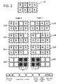
- Fig. 2 illustrates a preferred example of a data encoding scheme in accordance with the invention.
- two adjacent blocks of four pixels of a standard Bayer pattern colour filter mosaic with each block including two green pixels, G, a red pixel, R, and a blue pixel, B, as described above.
- Binary data can be encoded in the colour filter mosaic applied to the border pixels as logic zeroes and ones as shown at 32A and 32B, 34A and 34B, and 36A and 36B respectively.
- a logical 0 is encoded at 32A by omitting the red colour filter element from right hand block and a logical 1 is encoded at 32B by omitting the red colour filter element from the left hand block.
- binary data may be encoded in the colour processing by varying the colour processing applied to individual border pixels in any way which may be discriminated when signals are read out from the pixels. This may be done by omission of any one colour element or combinations of colour elements. Alternatively, instead of omitting a colour element, multiple colours may be applied to the same pixel, making the filter element substantially or completely opaque.
- 34A/B shows a logic 0 and logic 1 encoded by omission of green filter elements
- 36A/B shows a logic 0 and logic 1 encoded by omission of blue filter elements.
- Red, green and blue coding of the type illustrated may be combined in the same colour filter mosaic.
- data may be encoded in the microlens array applied to the sensor. This is illustrated at 38A and 38B, where a logic 0 is encoded by omitting microlenses 40 from the left hand block of pixels and a logic 1 is encoded by omitting microlenses 40 from the right hand block of pixels.
- any type of data may be encoded using the method of the present invention.
- the invention is particularly intended for encoding colour process information and/or mask revision information, preferably in combination with a product code.
- the relevant information requires a relatively small number of bits.
- An example is illustrated at 42 in Fig. 2, where the data comprises a start code of 4 bits (one "nibble"), a product code comprising three nibbles (3 x 4 bits), a colour process code of four bits, a mask revision code of four bits and an end code of 4 bits. This data is easily accommodated in the number of border pixels available in a typical image sensor.
- the data encoded in the colour processing may be read at any time during the life of the sensor by illuminating the sensor and interpreting the output from the border pixels.
- Algorithms for reading the data may be incorporated in the sensor or sensor system or may be provided separately from the sensor/system.
- the sensor or system circuitry is provided with storage means for electronically storing the data read from the border pixels so that the data is available for use by signal processing algorithms during subsequent use of the image sensor/system.
Landscapes
- Color Television Image Signal Generators (AREA)
- Solid State Image Pick-Up Elements (AREA)
Abstract
Description
- The present invention relates to encoding reference data in solid state image sensors. More particularly, the invention relates to encoding data in the colour processing applied to border pixels of the imaging array of a colour image sensor. The invention may be employed to encode any type of reference data, but is particularly useful for recording colour process and mask revision codes.
- It is well known to record reference data on a variety of types of microchip, including solid state image sensors, during manufacture of the chips. Such data may include product codes and the like, and may be encoded in the chip circuitry using a variety of coding schemes. In the case of an image sensor, such reference data may for example identify the particular type of the basic sensor chip. However, the same basic chip may provide the basis for a variety of different image sensors which differ in terms of the "colour processing" applied to the basic chip. The details of the colour processing determine the characteristics of, for example, the colour filter mosaic and microlens array applied to the chip. It is not practical to record such data in the chip circuitry during manufacture of the basic chip since the details of the subsequent colour processing may not be known at the time of basic chip manufacture.
- Solid state image sensors generally comprise an array of light sensitive elements ("pixels") arranged in rows and columns, together with associated circuitry for reading out signals from the pixel array. All of the pixels of the array are connected to the associated circuitry and are capable of being "read", but a number (typically two to eight) of the rows and columns of pixels around the periphery of the pixel array are not actually used in the image signals output from the sensor. These unused pixels are commonly referred to as "border pixels".
- The invention, in its various aspects, is defined in the Claims appended hereto.
- Embodiments of the invention will now be described, by way of example only, with reference to the accompanying drawings, in which:
- Fig. 1 is a schematic block diagram illustrating a generic solid state image sensor or image sensing system; and
- Fig. 2 is a diagram illustrating an embodiment of a data coding scheme in accordance with the present invention.
-
- Referring now to the drawings, Fig. 1 shows a generic solid state image sensor/sensing system comprising: a
sensor array 10 comprising an array of photosensitive pixels arranged in lines and columns; vertical andhorizontal shift registers sensor array 10; control means 16 for controlling the operation of theshift registers array 10, which are output via thehorizontal shift register 14. The arrangement of the sensor as described thus far is generic for a variety of conventional image sensors and will not be described in detail. It will be understood that the control means 16 and signal processing means 18 may be implemented in hardware, firmware or software and may be integrated on-chip with thesensor array 10, or located off-chip, locally or remotely, or combinations thereof. Generally speaking, the input to the signal processing means 18 will be analog, and the signal processing means may include analog-digital-conversion means, digital signal processing means for a performing any of a variety of signal processing functions as are well known in the art, and storage means for storing one or more images and/or portions of images for a variety of purposes. - As is well known in the art, the pixels of a number of rows and columns around the periphery of the
pixel array 10, typically two to eight rows/columns, are designated as "border pixels", indicated byreference numeral 20 in Fig. 1. The border pixels are fully functional pixels but, in normal use of the sensor, they are either not read or their output signals are ignored; i.e. their outputs do not form part of the image signal produced by the sensor. - It is known to encode data, such as product codes, in the electronic circuitry of the basic sensor chip during manufacture thereof.
- As is also well known in the art, a colour image sensor is produced by applying "colour processing" to a basic sensor chip of the type described above. Typically, colour processing involves the application of a colour filter mosaic to the
pixel array 10. Colour processing may also include the application of a microlens array on top of the colour filter mosaic, to improve the light gathering capacity of the pixels. - The colour filter mosaic may have any of a variety of well known configurations, using a variety of different colour combinations, typically three primary colours such as red, green and blue or complementary colours such as cyan, magenta and yellow, in order to produce a full colour image output from the sensor. One example of a colour filter pattern is the well known "Bayer Pattern", in which the pixels of the
basic array 10 are grouped in blocks of four, with the pixels at two diagonally opposite corners of each block being coloured green and the remaining two pixels being coloured red and blue respectively. - It is common for a number of different colour processes having different parameters to be applied to basic sensor chips of the same type. It is also common for different versions ("revisions") of a colour process mask to be employed. It is useful for the sensor to have information recorded thereon regarding the colour process applied and/or mask revision employed on that particular sensor. It is not practical to encode such data in the circuitry of the basic chip during manufacture thereof.
- In accordance with the present invention, data is encoded in the colour processing applied to at least some of the border pixels of the basic sensor chip, such that the recorded data may be read during manufacture of the sensor, subsequent assembly of an imaging system employing the sensor, or subsequent use of the sensor.
- Fig. 2 illustrates a preferred example of a data encoding scheme in accordance with the invention. At 30 there are shown two adjacent blocks of four pixels of a standard Bayer pattern colour filter mosaic, with each block including two green pixels, G, a red pixel, R, and a blue pixel, B, as described above. Binary data can be encoded in the colour filter mosaic applied to the border pixels as logic zeroes and ones as shown at 32A and 32B, 34A and 34B, and 36A and 36B respectively.
- In this example, a logical 0 is encoded at 32A by omitting the red colour filter element from right hand block and a logical 1 is encoded at 32B by omitting the red colour filter element from the left hand block. When the sensor is illuminated by incident light and signals are read out from the relevant pixels, it is possible to discriminate between a signal from a pixel having a colour filter element and a pixel with no colour filter element. The manner in which such signals may be discriminated is well known in the art (e.g. from error detection algorithms used in conventional image sensors) and will not be described in detail herein.
- It will be understood that binary data may be encoded in the colour processing by varying the colour processing applied to individual border pixels in any way which may be discriminated when signals are read out from the pixels. This may be done by omission of any one colour element or combinations of colour elements. Alternatively, instead of omitting a colour element, multiple colours may be applied to the same pixel, making the filter element substantially or completely opaque.
- 34A/B shows a
logic 0 andlogic 1 encoded by omission of green filter elements, whilst 36A/B shows alogic 0 andlogic 1 encoded by omission of blue filter elements. Red, green and blue coding of the type illustrated may be combined in the same colour filter mosaic. - Alternatively or in addition to encoding data in the colour filter mosaic pattern, data may be encoded in the microlens array applied to the sensor. This is illustrated at 38A and 38B, where a
logic 0 is encoded by omittingmicrolenses 40 from the left hand block of pixels and alogic 1 is encoded by omittingmicrolenses 40 from the right hand block of pixels. - Any type of data may be encoded using the method of the present invention. However, the invention is particularly intended for encoding colour process information and/or mask revision information, preferably in combination with a product code. The relevant information requires a relatively small number of bits. An example is illustrated at 42 in Fig. 2, where the data comprises a start code of 4 bits (one "nibble"), a product code comprising three nibbles (3 x 4 bits), a colour process code of four bits, a mask revision code of four bits and an end code of 4 bits. This data is easily accommodated in the number of border pixels available in a typical image sensor.
- It will be understood that the coding scheme employed may vary from the illustrated examples and may be adapted for use with any type of colour filter mosaic or microlens array.
- The data encoded in the colour processing may be read at any time during the life of the sensor by illuminating the sensor and interpreting the output from the border pixels. Algorithms for reading the data may be incorporated in the sensor or sensor system or may be provided separately from the sensor/system. Preferably, the sensor or system circuitry is provided with storage means for electronically storing the data read from the border pixels so that the data is available for use by signal processing algorithms during subsequent use of the image sensor/system.
- Improvements and modifications may be incorporated without departing from the scope of the invention.
Claims (16)
- A method of encoding data in a solid state image sensor, said sensor comprising an array of pixels including a plurality of border pixels with colour processing applied to said array of pixels, the method comprising varying the colour processing applied to at least some of said border pixels in accordance with a predetermined scheme such that data is encoded in the colour processing applied to said border pixels.
- A method as claimed in claim 1, wherein the colour processing includes the application of a colour filter mosaic to said array of pixels and said data is encoded by means of varying the pattern of colour filter material applied to said border pixels.
- A method as claimed in claim 2, wherein said data is encoded by the omission of colour filter material from selected border pixels.
- A method as claimed in claim 2, wherein said data is encoded by the application of multiple colour filter layers to selected border pixels.
- A method as claimed in any one of claims 2 to 4, wherein said colour filter mosaic comprises a Bayer pattern mosaic and wherein one bit of binary data is encoded in two adjacent blocks of four pixels of said pattern by varying the colour filter material applied to one pixel of one of said two adjacent blocks.
- A method as claimed in claim 1, wherein the colour processing includes the application of a microlens array to said array of pixels and said data is encoded by means of varying the pattern of microlenses applied to said border pixels.
- A method according to any preceding claim, wherein the encoded data includes a colour process code.
- A method according to any preceding claim wherein the encoded data includes a mask revision code.
- A method according to any preceding claim, wherein the encoded data includes a product code.
- A method according to any preceding claim, wherein the encoded data includes at least one of a start code and an end code.
- A method of reading data encoded using the method of any one of claims 1 to 10, comprising illuminating the image sensor and interpreting signals output from said border pixels.
- A method as claimed in claim 11, further including a step of electronically storing said data in said image sensor or in an image sensor system incorporating said image sensor.
- A solid state image sensor comprising an array of pixels including a plurality of border pixels with colour processing applied to said array of pixels, said image sensor including data encoded in the colour processing applied to at least some of said border pixels.
- An image sensor as claimed in claim 13, wherein said data is encoded by means of a method as claimed in any one of claims 1 to 10.
- An image sensor as claimed in claim 13 or claim 14, or an image sensor system incorporating said image sensor, adapted to read said data encoded in said colour processing when the image sensor is illuminated.
- An image sensor or an image sensor system as claimed in claim 15, including storage means for electronically storing said data.
Priority Applications (3)
| Application Number | Priority Date | Filing Date | Title |
|---|---|---|---|
| EP01301123A EP1231647B1 (en) | 2001-02-08 | 2001-02-08 | Reference data coding in solid state image sensors |
| DE60134950T DE60134950D1 (en) | 2001-02-08 | 2001-02-08 | Reference data encoding for a solid-state imaging device |
| US10/072,460 US6812058B2 (en) | 2001-02-08 | 2002-02-07 | Reference data coding in solid state image sensors |
Applications Claiming Priority (1)
| Application Number | Priority Date | Filing Date | Title |
|---|---|---|---|
| EP01301123A EP1231647B1 (en) | 2001-02-08 | 2001-02-08 | Reference data coding in solid state image sensors |
Publications (2)
| Publication Number | Publication Date |
|---|---|
| EP1231647A1 true EP1231647A1 (en) | 2002-08-14 |
| EP1231647B1 EP1231647B1 (en) | 2008-07-23 |
Family
ID=8181698
Family Applications (1)
| Application Number | Title | Priority Date | Filing Date |
|---|---|---|---|
| EP01301123A Expired - Lifetime EP1231647B1 (en) | 2001-02-08 | 2001-02-08 | Reference data coding in solid state image sensors |
Country Status (3)
| Country | Link |
|---|---|
| US (1) | US6812058B2 (en) |
| EP (1) | EP1231647B1 (en) |
| DE (1) | DE60134950D1 (en) |
Cited By (1)
| Publication number | Priority date | Publication date | Assignee | Title |
|---|---|---|---|---|
| EP1547150A4 (en) * | 2002-08-27 | 2006-12-06 | Phocus Inc E | PHOTOCONDUCTOR ON ACTIVE PIXEL IMAGE DETECTOR |
Families Citing this family (20)
| Publication number | Priority date | Publication date | Assignee | Title |
|---|---|---|---|---|
| US6791619B1 (en) * | 1998-09-01 | 2004-09-14 | Fuji Photo Film Co., Ltd. | System and method for recording management data for management of solid-state electronic image sensing device, and system and method for sensing management data |
| US6960753B2 (en) * | 2001-01-24 | 2005-11-01 | Hewlett-Packard Development Company, L.P. | Photosensor arrays with encoded permanent information |
| US6979588B2 (en) * | 2003-01-29 | 2005-12-27 | Hynix Semiconductor Inc. | Method for manufacturing CMOS image sensor having microlens therein with high photosensitivity |
| US6995914B1 (en) * | 2003-02-21 | 2006-02-07 | Conley Kenneth E | Method of producing a sheet having lenticular lens in pre-selected areas |
| US7522203B2 (en) * | 2003-10-01 | 2009-04-21 | Eastman Kodak Company | Electronic serialization of image sensors |
| US8654815B1 (en) | 2004-04-02 | 2014-02-18 | Rearden, Llc | System and method for distributed antenna wireless communications |
| US9819403B2 (en) | 2004-04-02 | 2017-11-14 | Rearden, Llc | System and method for managing handoff of a client between different distributed-input-distributed-output (DIDO) networks based on detected velocity of the client |
| US10277290B2 (en) | 2004-04-02 | 2019-04-30 | Rearden, Llc | Systems and methods to exploit areas of coherence in wireless systems |
| US10425134B2 (en) | 2004-04-02 | 2019-09-24 | Rearden, Llc | System and methods for planned evolution and obsolescence of multiuser spectrum |
| US9826537B2 (en) | 2004-04-02 | 2017-11-21 | Rearden, Llc | System and method for managing inter-cluster handoff of clients which traverse multiple DIDO clusters |
| US10148897B2 (en) * | 2005-07-20 | 2018-12-04 | Rearden, Llc | Apparatus and method for capturing still images and video using coded lens imaging techniques |
| US8816460B2 (en) * | 2009-04-06 | 2014-08-26 | Nokia Corporation | Image sensor |
| US8134115B2 (en) * | 2009-06-23 | 2012-03-13 | Nokia Corporation | Color filters for sub-diffraction limit-sized light sensors |
| US8198578B2 (en) * | 2009-06-23 | 2012-06-12 | Nokia Corporation | Color filters for sub-diffraction limit-sized light sensors |
| US8179457B2 (en) * | 2009-06-23 | 2012-05-15 | Nokia Corporation | Gradient color filters for sub-diffraction limit sensors |
| US11189917B2 (en) | 2014-04-16 | 2021-11-30 | Rearden, Llc | Systems and methods for distributing radioheads |
| US10488535B2 (en) | 2013-03-12 | 2019-11-26 | Rearden, Llc | Apparatus and method for capturing still images and video using diffraction coded imaging techniques |
| US9923657B2 (en) | 2013-03-12 | 2018-03-20 | Rearden, Llc | Systems and methods for exploiting inter-cell multiplexing gain in wireless cellular systems via distributed input distributed output technology |
| US9973246B2 (en) | 2013-03-12 | 2018-05-15 | Rearden, Llc | Systems and methods for exploiting inter-cell multiplexing gain in wireless cellular systems via distributed input distributed output technology |
| RU2767777C2 (en) | 2013-03-15 | 2022-03-21 | Риарден, Ллк | Systems and methods of radio frequency calibration using the principle of reciprocity of channels in wireless communication with distributed input - distributed output |
Citations (7)
| Publication number | Priority date | Publication date | Assignee | Title |
|---|---|---|---|---|
| JPS57141850A (en) * | 1981-02-27 | 1982-09-02 | Hitachi Ltd | Color separation filter element for image pickup tube and its manufacture |
| JPS6385704A (en) * | 1986-09-30 | 1988-04-16 | Toppan Printing Co Ltd | Production of color filter |
| JPH01137201A (en) * | 1987-11-25 | 1989-05-30 | Toppan Printing Co Ltd | Production of color solid-state image pickup element |
| JPH05164914A (en) * | 1991-12-19 | 1993-06-29 | Matsushita Electron Corp | Color solid image pickup device |
| JPH11101907A (en) * | 1997-09-26 | 1999-04-13 | Dainippon Printing Co Ltd | Color filter and color filter manufacturing management system |
| JPH11119204A (en) * | 1997-10-16 | 1999-04-30 | Toray Ind Inc | Substrate with color filter |
| WO1999050914A1 (en) * | 1998-03-31 | 1999-10-07 | Intel Corporation | Color microlenses and a method for creating |
Family Cites Families (3)
| Publication number | Priority date | Publication date | Assignee | Title |
|---|---|---|---|---|
| ATE161352T1 (en) * | 1992-09-04 | 1998-01-15 | Canon Kk | METHOD AND DEVICE FOR CONTROLLING A DISPLAY |
| US5353061A (en) * | 1992-10-08 | 1994-10-04 | International Business Machines Corporation | System and method for frame-differencing video compression/decompression using perceptually-constant information and image analysis |
| JP3462736B2 (en) * | 1997-11-17 | 2003-11-05 | ペンタックス株式会社 | Solid-state imaging device |
-
2001
- 2001-02-08 DE DE60134950T patent/DE60134950D1/en not_active Expired - Fee Related
- 2001-02-08 EP EP01301123A patent/EP1231647B1/en not_active Expired - Lifetime
-
2002
- 2002-02-07 US US10/072,460 patent/US6812058B2/en not_active Expired - Lifetime
Patent Citations (7)
| Publication number | Priority date | Publication date | Assignee | Title |
|---|---|---|---|---|
| JPS57141850A (en) * | 1981-02-27 | 1982-09-02 | Hitachi Ltd | Color separation filter element for image pickup tube and its manufacture |
| JPS6385704A (en) * | 1986-09-30 | 1988-04-16 | Toppan Printing Co Ltd | Production of color filter |
| JPH01137201A (en) * | 1987-11-25 | 1989-05-30 | Toppan Printing Co Ltd | Production of color solid-state image pickup element |
| JPH05164914A (en) * | 1991-12-19 | 1993-06-29 | Matsushita Electron Corp | Color solid image pickup device |
| JPH11101907A (en) * | 1997-09-26 | 1999-04-13 | Dainippon Printing Co Ltd | Color filter and color filter manufacturing management system |
| JPH11119204A (en) * | 1997-10-16 | 1999-04-30 | Toray Ind Inc | Substrate with color filter |
| WO1999050914A1 (en) * | 1998-03-31 | 1999-10-07 | Intel Corporation | Color microlenses and a method for creating |
Non-Patent Citations (5)
| Title |
|---|
| PATENT ABSTRACTS OF JAPAN vol. 006, no. 243 (E - 145) 2 December 1982 (1982-12-02) * |
| PATENT ABSTRACTS OF JAPAN vol. 012, no. 323 (P - 752) 2 September 1988 (1988-09-02) * |
| PATENT ABSTRACTS OF JAPAN vol. 013, no. 389 (P - 925) 29 August 1989 (1989-08-29) * |
| PATENT ABSTRACTS OF JAPAN vol. 017, no. 566 (P - 1629) 14 October 1993 (1993-10-14) * |
| PATENT ABSTRACTS OF JAPAN vol. 1999, no. 09 30 July 1999 (1999-07-30) * |
Cited By (1)
| Publication number | Priority date | Publication date | Assignee | Title |
|---|---|---|---|---|
| EP1547150A4 (en) * | 2002-08-27 | 2006-12-06 | Phocus Inc E | PHOTOCONDUCTOR ON ACTIVE PIXEL IMAGE DETECTOR |
Also Published As
| Publication number | Publication date |
|---|---|
| US20020114526A1 (en) | 2002-08-22 |
| US6812058B2 (en) | 2004-11-02 |
| DE60134950D1 (en) | 2008-09-04 |
| EP1231647B1 (en) | 2008-07-23 |
Similar Documents
| Publication | Publication Date | Title |
|---|---|---|
| EP1231647B1 (en) | Reference data coding in solid state image sensors | |
| CN101546386B (en) | QR code with a rectangular area with a specific pattern used to designate the location of the cell and distinguish it from the background | |
| EP0864229B1 (en) | Optoelectronic sensor with shuffled readout | |
| JP3996520B2 (en) | Two-dimensional information code and generation method thereof | |
| EP0764944A2 (en) | Information recording medium for recording multimedia information as optical readable code data thereon and information recording reproducing system using the same | |
| US7061533B1 (en) | Image processing apparatus | |
| US20080186395A1 (en) | Photo diode fuse-id for cmos imagers | |
| WO1998050882A2 (en) | Multi-colored symbology method and apparatus | |
| JP5115404B2 (en) | 2D code | |
| JP5133766B2 (en) | Imaging device | |
| US7292278B2 (en) | System and method for recording management data for management of solid-state electronic image sensing device, and system and method for sensing management data | |
| US7027091B1 (en) | Detection of color filter array alignment in image sensors | |
| KR19990063471A (en) | Imaging device | |
| CN112019823B (en) | A filter array and an image sensor | |
| US6960753B2 (en) | Photosensor arrays with encoded permanent information | |
| US7401738B2 (en) | Apparatus for reading a color symbol | |
| JP4241803B2 (en) | Two-dimensional information code reading method and reading apparatus | |
| JP7415399B2 (en) | Information code, information code medium, information code generation method, and information code reading device | |
| JP5267323B2 (en) | Two-dimensional code reader | |
| EP1605686B1 (en) | Solid state image sensor | |
| JP5195622B2 (en) | Two-dimensional information code | |
| CN100498829C (en) | Media with index data and system for reading the media with index data | |
| JP4095181B2 (en) | Black ink use determination method and black ink use determination device | |
| JP4222361B2 (en) | Information code reader and luminance signal generation method | |
| JP2025070915A (en) | Method for increasing information added to identification codes |
Legal Events
| Date | Code | Title | Description |
|---|---|---|---|
| PUAI | Public reference made under article 153(3) epc to a published international application that has entered the european phase |
Free format text: ORIGINAL CODE: 0009012 |
|
| AK | Designated contracting states |
Kind code of ref document: A1 Designated state(s): AT BE CH CY DE DK ES FI FR GB GR IE IT LI LU MC NL PT SE TR |
|
| AX | Request for extension of the european patent |
Free format text: AL;LT;LV;MK;RO;SI |
|
| 17P | Request for examination filed |
Effective date: 20030110 |
|
| AKX | Designation fees paid |
Designated state(s): DE FR GB IT |
|
| 17Q | First examination report despatched |
Effective date: 20060320 |
|
| 17Q | First examination report despatched |
Effective date: 20060320 |
|
| GRAP | Despatch of communication of intention to grant a patent |
Free format text: ORIGINAL CODE: EPIDOSNIGR1 |
|
| GRAS | Grant fee paid |
Free format text: ORIGINAL CODE: EPIDOSNIGR3 |
|
| GRAA | (expected) grant |
Free format text: ORIGINAL CODE: 0009210 |
|
| AK | Designated contracting states |
Kind code of ref document: B1 Designated state(s): DE FR GB IT |
|
| REG | Reference to a national code |
Ref country code: GB Ref legal event code: FG4D |
|
| REF | Corresponds to: |
Ref document number: 60134950 Country of ref document: DE Date of ref document: 20080904 Kind code of ref document: P |
|
| PLBE | No opposition filed within time limit |
Free format text: ORIGINAL CODE: 0009261 |
|
| STAA | Information on the status of an ep patent application or granted ep patent |
Free format text: STATUS: NO OPPOSITION FILED WITHIN TIME LIMIT |
|
| 26N | No opposition filed |
Effective date: 20090424 |
|
| PG25 | Lapsed in a contracting state [announced via postgrant information from national office to epo] |
Ref country code: IT Free format text: LAPSE BECAUSE OF FAILURE TO SUBMIT A TRANSLATION OF THE DESCRIPTION OR TO PAY THE FEE WITHIN THE PRESCRIBED TIME-LIMIT Effective date: 20080723 |
|
| PG25 | Lapsed in a contracting state [announced via postgrant information from national office to epo] |
Ref country code: DE Free format text: LAPSE BECAUSE OF NON-PAYMENT OF DUE FEES Effective date: 20090901 |
|
| REG | Reference to a national code |
Ref country code: FR Ref legal event code: PLFP Year of fee payment: 16 |
|
| REG | Reference to a national code |
Ref country code: FR Ref legal event code: PLFP Year of fee payment: 17 |
|
| REG | Reference to a national code |
Ref country code: FR Ref legal event code: PLFP Year of fee payment: 18 |
|
| PGFP | Annual fee paid to national office [announced via postgrant information from national office to epo] |
Ref country code: GB Payment date: 20200123 Year of fee payment: 20 |
|
| PGFP | Annual fee paid to national office [announced via postgrant information from national office to epo] |
Ref country code: FR Payment date: 20200122 Year of fee payment: 20 |
|
| REG | Reference to a national code |
Ref country code: GB Ref legal event code: PE20 Expiry date: 20210207 |
|
| PG25 | Lapsed in a contracting state [announced via postgrant information from national office to epo] |
Ref country code: GB Free format text: LAPSE BECAUSE OF EXPIRATION OF PROTECTION Effective date: 20210207 |