EP1231630A2 - Method of fabricating ferroelectric memory transistors - Google Patents
Method of fabricating ferroelectric memory transistors Download PDFInfo
- Publication number
- EP1231630A2 EP1231630A2 EP02250979A EP02250979A EP1231630A2 EP 1231630 A2 EP1231630 A2 EP 1231630A2 EP 02250979 A EP02250979 A EP 02250979A EP 02250979 A EP02250979 A EP 02250979A EP 1231630 A2 EP1231630 A2 EP 1231630A2
- Authority
- EP
- European Patent Office
- Prior art keywords
- depositing
- electrode
- forming
- ferroelectric
- electrode plug
- Prior art date
- Legal status (The legal status is an assumption and is not a legal conclusion. Google has not performed a legal analysis and makes no representation as to the accuracy of the status listed.)
- Withdrawn
Links
Images




Classifications
-
- H—ELECTRICITY
- H10—SEMICONDUCTOR DEVICES; ELECTRIC SOLID-STATE DEVICES NOT OTHERWISE PROVIDED FOR
- H10D—INORGANIC ELECTRIC SEMICONDUCTOR DEVICES
- H10D84/00—Integrated devices formed in or on semiconductor substrates that comprise only semiconducting layers, e.g. on Si wafers or on GaAs-on-Si wafers
- H10D84/80—Integrated devices formed in or on semiconductor substrates that comprise only semiconducting layers, e.g. on Si wafers or on GaAs-on-Si wafers characterised by the integration of at least one component covered by groups H10D12/00 or H10D30/00, e.g. integration of IGFETs
-
- H—ELECTRICITY
- H10—SEMICONDUCTOR DEVICES; ELECTRIC SOLID-STATE DEVICES NOT OTHERWISE PROVIDED FOR
- H10D—INORGANIC ELECTRIC SEMICONDUCTOR DEVICES
- H10D30/00—Field-effect transistors [FET]
- H10D30/01—Manufacture or treatment
- H10D30/021—Manufacture or treatment of FETs having insulated gates [IGFET]
- H10D30/0415—Manufacture or treatment of FETs having insulated gates [IGFET] of FETs having ferroelectric gate insulators
-
- H—ELECTRICITY
- H10—SEMICONDUCTOR DEVICES; ELECTRIC SOLID-STATE DEVICES NOT OTHERWISE PROVIDED FOR
- H10D—INORGANIC ELECTRIC SEMICONDUCTOR DEVICES
- H10D30/00—Field-effect transistors [FET]
- H10D30/60—Insulated-gate field-effect transistors [IGFET]
- H10D30/701—IGFETs having ferroelectric gate insulators, e.g. ferroelectric FETs
-
- H—ELECTRICITY
- H10—SEMICONDUCTOR DEVICES; ELECTRIC SOLID-STATE DEVICES NOT OTHERWISE PROVIDED FOR
- H10D—INORGANIC ELECTRIC SEMICONDUCTOR DEVICES
- H10D64/00—Electrodes of devices having potential barriers
- H10D64/01—Manufacture or treatment
- H10D64/031—Manufacture or treatment of data-storage electrodes
- H10D64/033—Manufacture or treatment of data-storage electrodes comprising ferroelectric layers
Definitions
- This invention relates to the manufacture of transistors incorporating ferroelectric thin films therein, and specifically to fabrication of a metal/ferro/metal/oxide/semiconductor (MFMOS) and metal/ferro/metal/semiconductor (MFMS) transistors using a nitride replacement technique.
- MMOS metal/ferro/metal/oxide/semiconductor
- MFMS metal/ferro/metal/semiconductor
- Ferroelectric thin films are used in nonvolatile memories.
- Metal-ferroelectric-metal-silicon semi-conductors also referred to herein as ferroelectric memory (FEM) cells are particularly useful as memory transistors.
- FRAM ferroelectric random access memories
- Known ferroelectric random access memories (FRAM) are constructed with one transistor (1T) and one capacitor (1C).
- the capacitor is generally made by sandwiching a thin ferroelectric film between two conductive electrodes, which electrodes are usually made of platinum.
- the circuit configuration and the read/write sequence of this type of memory are similar to that of convention dynamic random access memories (DRAM), except that no data refreshing is necessary in a FRAM.
- DRAM convention dynamic random access memories
- ferroelectric-gate-controlled field effect transistor FET
- FET ferroelectric-gate controlled field effect transistor
- MFS metal-ferroelectric-silicon
- FRAMs incorporating the MFS FET structure have two major advantages over the transistor-capacitor configuration: (1) The MFS FET occupies less surface area, and (2) provides a non-destructive readout (NDR). The latter feature enables a MFS FET device to be read thousands of times without switching the ferroelectric polarization.
- MFS FET structures may be constructed, such as metal/ferroelectric/insulators/silicon (MFIS) FET, metal/ferroelectric/metal/semiconductor (MFMS) FET, and metal/ferroelectric/metal/oxide/semiconductor (MFMOS) FET.
- MFIS metal/ferroelectric/insulators/silicon
- MFMS metal/ferroelectric/metal/semiconductor
- MMOS metal/ferroelectric/metal/oxide/semiconductor
- the etching does not extend significantly into the silicon.
- the thickness of the gate oxide of a MFMOS memory transistor is very thin, and it is exceptionally difficult to stop the gate stack etching process at the level of the gate oxide. Large source/drain series resistances may occur if excessive amounts of silicon are consumed by the gate stack etching process.
- the surface channel is very shallow. This channel may be completely removed by etching during the gate stack etching process if proper controls are not maintained.
- a method of fabricating a ferroelectric memory transistor includes preparing a substrate, including isolating an active region; forming a gate region; depositing an electrode plug in the gate region; depositing an oxide side wall about the electrode plug; implanting Arsenic ions to form a source region and a drain region; annealing a structure obtained by the above-described steps to diffuse the implanted ions; depositing an intermediate oxide layer over the structure; removing the electrode plug; depositing a bottom electrode in place of the electrode plug; depositing a ferroelectric layer over the bottom electrode; depositing a top electrode over the ferroelectric layer; depositing a protective layer; depositing a passivation oxide layer over the structure; and metallizing the structure.
- Another object of the invention to provide a method of fabricating MFMOS memory transistors and MFMS memory transistors which will reduce fabrication cost and increase production output.
- the etching processes used to etch the gate stack of metal/ferro metal oxide semiconductor (MFMOS) and metal/ferro metal semiconductor (MFMS) memory transistors frequently consume too much silicon during the etching process, particularly in the case of MFMOS memory transistor. wherein the gate oxide is very thin. It is very difficult to stop the gate stack etching process at the level of the gate oxide. Large source/drain series resistances, on the order of 1,000 ohms, may occur when excessive consumption of silicon occurs during the gate stack etching process. In the case of MFMS memory transistors, the surface channel is very shallow, and may be completely removed during the gate stack etching process.
- the method of the invention provides a method for fabricating MFMOS memory transistors and MFMS memory transistors without the requirement for exceptionally precise gate stack etching techniques.
- the method of the invention includes forming the bottom electrode of the gate stack by a nitride replacement process, which allows the bottom electrode of the gate stack to remain flat.
- a nitride replacement process which allows the bottom electrode of the gate stack to remain flat.
- an ultra thin gate oxide may be provided for MFMOS memory transistors, and an ultra shallow surface conducting channel may be incorporated into MFMS memory transistors.
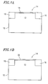
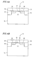
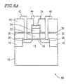
- the steps in the fabrication of the structure for a MFMOS memory transistors and for a MFMS memory transistors are depicted in Figs. 1A-6A and Figs. 1B-6B, respectively.
- the steps used to fabricate both types of devices are sufficiently similar that they will be described simultaneously.
- a p-type substrate 10 for well formation 12 by implantation of Boron ions, at a dose of about 1 ⁇ 10 12 cm -2 to 1 ⁇ 10 13 cm -2 , and at an energy level of 30 keV to 50 keV, threshold voltage adjustment of an active region 14, active device isolation by oxide 16, and gate oxidation 18 for MFMOS memory transistor or surface channel formation 20 for MFMS memory transistor.
- LDD low doping density
- An oxide layer is deposited by CVD, to a thickness of about between 20 nm to 150 nm for the MFMOS memory transistor and to a thickness of about between 100 nm to 200 nm for the MFMS memory transistor.
- the structure is masked and etched, leaving a wall oxide 24 about electrode plug 22.
- a source region 26 and a drain region 28 are formed by implantation of Arsenic ions, at a dose of about 1 ⁇ 10 15 cm -2 to 5 ⁇ 10 15 cm -2 , and at an energy level of 30 keV to 70 keV.
- the structure is annealed, to provide ion diffusion, at a temperature of between about 700°C to 950°C for about 30 minutes to activate the N+ implanted ions in source region 26 and drain region 28.
- an intermediate oxide layer 30 is deposited by CVD, to a thickness which is at least 150% thicker than the thickness of electrode plug 22.
- Intermediate oxide layer 30 and silicon nitride 22 are smoothed and thinned by chemical mechanical polishing (CMP). The silicon nitride is then wet etched completely to remove the electrode plug, resulting in the structure shown in Figs. 3A and 3B.
- a bottom electrode 32 of Indium is deposited, and smoothed by CMP, as shown in Figs. 4A and 4B.
- a ferroelectric thin film 34 and a top electrode 36 are deposited. Photoresist is applied over the gate stack, and the top electrode and ferroelectric are etched. The photoresist is then removed. A protection film 38, such as TiO 2 , or silicon nitride, is deposited to a thickness of between about 10 nm to 30 nm.
- the remaining process steps include CVD of a passivation oxide layer 40, and metallization to form a source electrode 42, a gate electrode 44 and a drain electrode 46, which steps may be performed using state-of-the-art processes, resulting in a final MFMOS memory transistor device 48, as shown in Fig. 6A, and a final MFMS memory transistor device 50, as shown in Fig. 6B.
Landscapes
- Semiconductor Memories (AREA)
- Non-Volatile Memory (AREA)
- Metal-Oxide And Bipolar Metal-Oxide Semiconductor Integrated Circuits (AREA)
Abstract
Description
Claims (13)
- A method of fabricating a ferroelectric memory transistor comprising:a) preparing a substrate, including isolating an active region;b) forming a gate region;c) depositing an electrode plug in the gate region;d) depositing an oxide side wall about the electrode plug;e) implanting Arsenic ions to form a source region and a drain region;f) annealing a structure obtained by the steps a) to e) to diffuse the implanted ions;g) depositing an intermediate oxide layer over the structure;h) removing the electrode plug;i) depositing a bottom electrode in place of the electrode plug;j) depositing a ferroelectric layer over the bottom electrode;k) depositing a top electrode over the ferroelectric layer;l) depositing a protected layer;m) depositing a passivation oxide layer over the structure; andn) metallizing the structure.
- The method of claim 1 wherein said b) forming a gate region includes oxidizing silicon of the substrate.
- The method of claim wherein said b) forming a gate region includes forming a surface channel.
- The method of claim 1 which further includes LDD implantation of Arsenic ions, at an energy level of 10 keV to 30 keV and a dose of 5·1012 cm-2 to 5·1013 cm-2.
- The method of claim 1 wherein said e) implanting includes implanting Arsenic ions, at a dose of about 1·1015 cm-2 to 5·1015 cm-2, and at an energy level of 30 keV to 70 keV and wherein said f) annealing includes annealing the structure at a temperature of between about 700°C to 950°C for about 30 minutes.
- The method of claim 1 wherein said 1) depositing a protective layer includes depositing a layer of material taken from the group of materials consisting of TiO2 and silicon nitride to a thickness of between about 10 nm and 30 nm.
- A method of fabricating a ferroelectric memory transistor comprising:a) preparing a substrate, including isolating an active region;b) forming a gate region;c) depositing an electrode plug of silicon nitride to a thickness of between about 200 nm and 300 nm in the gate region;d) depositing an oxide layer about the electrode plug and etching the oxide layer to form a sidewall oxide about the electrode plug;e) implanting Arsenic ions, at a dose of about 1·1015 cm-2 to 5·1015 cm-2, and at an energy level of 30 keV to 70 keV to form a source region and a drain region, and annealing a structure obtained by the steps a)-d) at a temperature of between about 700°C to 950°C for about 30 minutes to diffuse the implanted ions;f) depositing an intermediate oxide layer over the structure, wherein said depositing includes depositing the intermediate layer to a thickness of at least 150% greater than that of the electrode plug;g) smoothing the structure by CMP;h) etching the electrode plug completely to remove the electrode plug;i) depositing a bottom electrode in place of the electrode plug;j) depositing a ferroelectric layer over the bottom electrode;k) depositing a top electrode over the ferroelectric layer;l) depositing a protective layer:m) depositing a passivation oxide layer over the structure; andn) metallizing the structure.
- The method of claim 7 wherein said b) forming a gate region includes oxidizing silicon of the substrate.
- The method of claim 7 wherein said b) forming a gate region includes forming a surface channel.
- The method of claim 7 which further includes LDD implantation of Arsenic ions, at an energy level of 10 keV to 30 keV and a dose of 5·1012 cm-2 to 5·1013 cm-2.
- The method of claim 7 wherein said 1) depositing a protective layer includes depositing a layer of material taken from the group of materials consisting of TiO2 and silicon nitride to a thickness of between about 10 nm to 30 nm.
- A method of fabricating a ferroelectric memory transistor in which a gate stack over a gate region in a substrate comprises a bottom electrode nearest to the substrate a top electrode and a ferroelectric layer disposed between the bottom and top electrode, wherein the bottom electrode is made bythe ferroelectric layer and the top electrode being formed by depositing corresponding films in sequence over the bottom electrode and removing unwanted portions of said corresponding films.forming an electrode plug over the gate region,forming an intermediate oxide layer over the structure,removing the electrode plug, andforming a bottom electrode in place of the electrode plug,
- A method of fabricating a ferroelectric memory transistor in which a bottom electrode in an electrode/ferroelectric/electrode stack is formed by replacing an electrode plug surrounded by an intermediate oxide film with an electrode material.
Applications Claiming Priority (2)
| Application Number | Priority Date | Filing Date | Title |
|---|---|---|---|
| US09/783,817 US6495377B2 (en) | 2001-02-13 | 2001-02-13 | Method of fabricating ferroelectric memory transistors |
| US783817 | 2001-02-13 |
Publications (2)
| Publication Number | Publication Date |
|---|---|
| EP1231630A2 true EP1231630A2 (en) | 2002-08-14 |
| EP1231630A3 EP1231630A3 (en) | 2004-12-29 |
Family
ID=25130477
Family Applications (1)
| Application Number | Title | Priority Date | Filing Date |
|---|---|---|---|
| EP02250979A Withdrawn EP1231630A3 (en) | 2001-02-13 | 2002-02-13 | Method of fabricating ferroelectric memory transistors |
Country Status (5)
| Country | Link |
|---|---|
| US (1) | US6495377B2 (en) |
| EP (1) | EP1231630A3 (en) |
| JP (1) | JP3916049B2 (en) |
| KR (1) | KR20020066966A (en) |
| TW (1) | TWI244727B (en) |
Cited By (1)
| Publication number | Priority date | Publication date | Assignee | Title |
|---|---|---|---|---|
| CN100380628C (en) * | 2005-04-18 | 2008-04-09 | 力晶半导体股份有限公司 | Method for manufacturing semiconductor element and method for manufacturing plug |
Families Citing this family (6)
| Publication number | Priority date | Publication date | Assignee | Title |
|---|---|---|---|---|
| US7378286B2 (en) * | 2004-08-20 | 2008-05-27 | Sharp Laboratories Of America, Inc. | Semiconductive metal oxide thin film ferroelectric memory transistor |
| US7524727B2 (en) | 2005-12-30 | 2009-04-28 | Intel Corporation | Gate electrode having a capping layer |
| US9059030B2 (en) * | 2011-10-07 | 2015-06-16 | Micron Technology, Inc. | Memory cells having capacitor dielectric directly against a transistor source/drain region |
| US11996462B2 (en) | 2020-11-13 | 2024-05-28 | Sandisk Technologies Llc | Ferroelectric field effect transistors having enhanced memory window and methods of making the same |
| US11545506B2 (en) | 2020-11-13 | 2023-01-03 | Sandisk Technologies Llc | Ferroelectric field effect transistors having enhanced memory window and methods of making the same |
| US20240088065A1 (en) * | 2022-09-08 | 2024-03-14 | International Business Machines Corporation | Ferroelectric memory device erasure |
Family Cites Families (6)
| Publication number | Priority date | Publication date | Assignee | Title |
|---|---|---|---|---|
| US5401680A (en) * | 1992-02-18 | 1995-03-28 | National Semiconductor Corporation | Method for forming a ceramic oxide capacitor having barrier layers |
| US5350705A (en) * | 1992-08-25 | 1994-09-27 | National Semiconductor Corporation | Ferroelectric memory cell arrangement having a split capacitor plate structure |
| US5858843A (en) * | 1996-09-27 | 1999-01-12 | Intel Corporation | Low temperature method of forming gate electrode and gate dielectric |
| US6051487A (en) * | 1997-12-18 | 2000-04-18 | Advanced Micro Devices, Inc. | Semiconductor device fabrication using a sacrificial plug for defining a region for a gate electrode |
| US6048740A (en) * | 1998-11-05 | 2000-04-11 | Sharp Laboratories Of America, Inc. | Ferroelectric nonvolatile transistor and method of making same |
| US6303502B1 (en) * | 2000-06-06 | 2001-10-16 | Sharp Laboratories Of America, Inc. | MOCVD metal oxide for one transistor memory |
-
2001
- 2001-02-13 US US09/783,817 patent/US6495377B2/en not_active Expired - Fee Related
-
2002
- 2002-01-22 JP JP2002013559A patent/JP3916049B2/en not_active Expired - Fee Related
- 2002-01-29 KR KR1020020005094A patent/KR20020066966A/en not_active Ceased
- 2002-02-04 TW TW091101888A patent/TWI244727B/en not_active IP Right Cessation
- 2002-02-13 EP EP02250979A patent/EP1231630A3/en not_active Withdrawn
Cited By (1)
| Publication number | Priority date | Publication date | Assignee | Title |
|---|---|---|---|---|
| CN100380628C (en) * | 2005-04-18 | 2008-04-09 | 力晶半导体股份有限公司 | Method for manufacturing semiconductor element and method for manufacturing plug |
Also Published As
| Publication number | Publication date |
|---|---|
| KR20020066966A (en) | 2002-08-21 |
| TWI244727B (en) | 2005-12-01 |
| US20020108927A1 (en) | 2002-08-15 |
| JP2002270791A (en) | 2002-09-20 |
| JP3916049B2 (en) | 2007-05-16 |
| US6495377B2 (en) | 2002-12-17 |
| EP1231630A3 (en) | 2004-12-29 |
Similar Documents
| Publication | Publication Date | Title |
|---|---|---|
| US5731608A (en) | One transistor ferroelectric memory cell and method of making the same | |
| EP0999597B1 (en) | Ferroelectric nonvolatile transistor and method of making same | |
| US4597060A (en) | EPROM array and method for fabricating | |
| JPH08264669A (en) | Ferroelectric memory device and manufacturing method thereof | |
| US5470776A (en) | Method for fabricating stacked dynamic random access memory cell | |
| EP0936675A2 (en) | C-axis oriented thin film ferroelectric transistor memory cell and method of making the same | |
| EP0869557B1 (en) | Ferroelectric memory cell and method of making the same | |
| US6703655B2 (en) | Ferroelectric memory transistor | |
| JPH0437170A (en) | Manufacturing method of semiconductor device | |
| US6146904A (en) | Method of making a two transistor ferroelectric memory cell | |
| US7244977B2 (en) | Longitudinal MISFET manufacturing method, longitudinal MISFET, semiconductor storage device manufacturing method, and semiconductor storage device | |
| US5949102A (en) | Semiconductor device having a gate electrode with only two crystal grains | |
| US6495377B2 (en) | Method of fabricating ferroelectric memory transistors | |
| US4713142A (en) | Method for fabricating EPROM array | |
| KR100470499B1 (en) | Method of making a self-aligned ferroelectric memory transistor | |
| US5942776A (en) | Shallow junction ferroelectric memory cell and method of making the same | |
| US6358798B1 (en) | Method for forming gate electrode by damascene process | |
| US6018171A (en) | Shallow junction ferroelectric memory cell having a laterally extending p-n junction and method of making the same | |
| US6762063B2 (en) | Method of fabricating non-volatile ferroelectric transistors | |
| US6455329B1 (en) | Method for fabricating a capacitor in a semiconductor device | |
| KR100289490B1 (en) | Method of forming semiconductor device having stepped insulating film | |
| KR100852236B1 (en) | Eeprom device and method of manufacturing the eeprom device | |
| US5943579A (en) | Method for forming a diffusion region in a semiconductor device | |
| KR960011472B1 (en) | Semiconductor Memory Manufacturing Method | |
| KR101099562B1 (en) | Method of manufacturing semiconductor device |
Legal Events
| Date | Code | Title | Description |
|---|---|---|---|
| PUAI | Public reference made under article 153(3) epc to a published international application that has entered the european phase |
Free format text: ORIGINAL CODE: 0009012 |
|
| AK | Designated contracting states |
Kind code of ref document: A2 Designated state(s): AT BE CH CY DE DK ES FI FR GB GR IE IT LI LU MC NL PT SE TR |
|
| AX | Request for extension of the european patent |
Free format text: AL;LT;LV;MK;RO;SI |
|
| PUAL | Search report despatched |
Free format text: ORIGINAL CODE: 0009013 |
|
| AK | Designated contracting states |
Kind code of ref document: A3 Designated state(s): AT BE CH CY DE DK ES FI FR GB GR IE IT LI LU MC NL PT SE TR |
|
| AX | Request for extension of the european patent |
Extension state: AL LT LV MK RO SI |
|
| 17P | Request for examination filed |
Effective date: 20050623 |
|
| AKX | Designation fees paid |
Designated state(s): DE FR GB |
|
| 17Q | First examination report despatched |
Effective date: 20071114 |
|
| STAA | Information on the status of an ep patent application or granted ep patent |
Free format text: STATUS: THE APPLICATION IS DEEMED TO BE WITHDRAWN |
|
| 18D | Application deemed to be withdrawn |
Effective date: 20080527 |