EP1229675A2 - Pump light source for raman amplifier and raman amplifier using the same - Google Patents

Pump light source for raman amplifier and raman amplifier using the same Download PDF

Info

Publication number
EP1229675A2
EP1229675A2 EP02250710A EP02250710A EP1229675A2 EP 1229675 A2 EP1229675 A2 EP 1229675A2 EP 02250710 A EP02250710 A EP 02250710A EP 02250710 A EP02250710 A EP 02250710A EP 1229675 A2 EP1229675 A2 EP 1229675A2
Authority
EP
European Patent Office
Prior art keywords
light source
light
lightwaves
pump
raman amplification
Prior art date
Legal status (The legal status is an assumption and is not a legal conclusion. Google has not performed a legal analysis and makes no representation as to the accuracy of the status listed.)
Withdrawn
Application number
EP02250710A
Other languages
German (de)
French (fr)
Other versions
EP1229675A3 (en
Inventor
Soko c/o The Furukawa Electric Co. Ltd. Kadao
Yoshihiro c/o The Furukawa Elec. Co. Ltd. Emori
Current Assignee (The listed assignees may be inaccurate. Google has not performed a legal analysis and makes no representation or warranty as to the accuracy of the list.)
Furukawa Electric Co Ltd
Original Assignee
Furukawa Electric Co Ltd
Priority date (The priority date is an assumption and is not a legal conclusion. Google has not performed a legal analysis and makes no representation as to the accuracy of the date listed.)
Filing date
Publication date
Application filed by Furukawa Electric Co Ltd filed Critical Furukawa Electric Co Ltd
Publication of EP1229675A2 publication Critical patent/EP1229675A2/en
Publication of EP1229675A3 publication Critical patent/EP1229675A3/en
Withdrawn legal-status Critical Current

Links

Images

Classifications

    • HELECTRICITY
    • H04ELECTRIC COMMUNICATION TECHNIQUE
    • H04BTRANSMISSION
    • H04B10/00Transmission systems employing electromagnetic waves other than radio-waves, e.g. infrared, visible or ultraviolet light, or employing corpuscular radiation, e.g. quantum communication
    • H04B10/29Repeaters
    • H04B10/291Repeaters in which processing or amplification is carried out without conversion of the main signal from optical form
    • H04B10/2912Repeaters in which processing or amplification is carried out without conversion of the main signal from optical form characterised by the medium used for amplification or processing
    • H04B10/2916Repeaters in which processing or amplification is carried out without conversion of the main signal from optical form characterised by the medium used for amplification or processing using Raman or Brillouin amplifiers

Definitions

  • the present invention relates to a pump light source for a Raman amplifier for optically amplifying signal lightwaves in a light transmission path such as an optical fiber by utilizing stimulated Raman scattering and to a Raman amplifier using the same.
  • an optical amplifier 5 when guiding an optical signal 2 output from a light transmitting station 1 to a light receiving station 4 through a light transmission path 3, such as an optical fiber, an optical amplifier 5 is arranged at some midpoint in the light transmission path 3 or at an end thereof to optically amplify the optical signal so that the optical signal 2, which has been attenuated in the light transmission path 3, may attain the requisite optical signal level for reception by the light receiving station 4.
  • the optical amplifier 5 is provided at the forward end or both ends of the light transmission path 3.
  • electrical information to be transmitted is converted into light to be output to the light transmission path 3.
  • An electric signal is converted to an optical signal by applying it directly to a semiconductor laser diode or the like serving as the signal light source or by modulating the light oscillated from the signal light source by an external modulator provided behind the signal light source before it is output to the light transmission path 3.
  • the optical signal 2 propagated through the light transmission path 3 is converted into an electric signal by a photoelectric converter, such as a photo diode, and the information transmitted from the light transmitting station 1 is demodulated, whereby the information is read.
  • a photoelectric converter such as a photo diode
  • oscillation light from a pump light source 7 is input to a Raman amplification medium 31 through an optical coupler 6 from an end portion of the Raman amplification medium 31 constituting a part of the light transmission path 3 to cause Raman scattering in the Raman amplification medium 31, thereby effecting Raman amplification on the optical signal 2.
  • the wavelength of the oscillation light to be selected is shorter than the wavelength of the optical signal 2 from the light transmitting station 1 by approximately 20 to 200 nm.
  • the Raman gain due to the Raman amplification in the Raman amplification medium 31 allows light amplification over a wide range. However, it does not allow uniform amplification over a wide signal band, exhibiting wavelength properties in amplification gain. Thus, to effect uniform Raman amplification over a wide signal band, a plurality of pump light sources of different wavelengths from each other are used in order to adjust the intensity of the pump lightwaves such that Raman gain is uniform over the signal band.
  • the above method in which the intensity of oscillation light of a plurality of light sources is adjusted has a problem in that the gain of a specific signal band is not adjusted by adjusting one of the plurality of light sources; it involves a change in the gain of a still wider signal band including the specific signal band, so that it is not easy to adjust the gain to a desired value.
  • the present inventor performed signal band gain measurement with the pump intensity of the semiconductor LD of 1460.265 nm reduced to 80%, 60%, 40%, and 20%, as shown in (10) through (13) of Table 2.
  • the results are the values indicated by the dotted lines (10) through (13) of Fig. 6. In these dotted lines, the gain at the shorter wavelength of the signal band does not vary compared with the gain at the longer wavelength, and the gain flatness is sufficient.
  • the present inventor divided pumps optimized so as to obtain flat gain properties in a certain signal band into Group A of the shorter wavelength and Group B of the longer wavelength to find out the following:
  • pump wavelengths are divided into two groups; the shorter wavelengths and the longer wavelengths, which are arbitrarily adjusted, whereby it is possible to obtain arbitrary gain properties.
  • a pump light source for outputting a plurality of pump lightwaves for effecting Raman amplification on signal lightwaves input to a light transmission path
  • the pump light source for Raman amplification is divided into light source whose oscillation wavelengths are the shorter (hereinafter referred to as “shorter wavelength light source) and light source whose oscillation wavelengths are the longer (hereinafter referred to as "longer wavelength light source); a plurality of lightwaves emitted from the shorter wavelength light source and a lightwave emitted from the longer wavelength light source are coupled and output; and the plurality of lightwaves output from the shorter wavelength light source or the lightwave output from the longer wavelength light source is collectively controlled to adjust the intensity of the output light.
  • a Raman amplifier including a light transmitting station for emitting signal lightwaves, a light receiving station for receiving the signal lightwaves, a light transmission path for propagating the signal lightwaves from the light transmitting station to the light receiving station, and a pump light source for Raman amplification which introduces pump lightwaves into the light transmission path to cause Raman scattering in the light transmission path to thereby effect Raman amplification on the signal lightwaves, wherein the pump light source for Raman amplification is as claimed in one of Claims 1 through 5.
  • Fig. 1 is a schematic diagram showing an embodiment of the present invention.
  • 31, 6, and 7 respectively indicate a Raman amplification medium, such as a silica-based optical fiber, an optical coupler for coupling pump lightwaves with signal lightwaves to be integrated in the Raman amplification medium, and a Raman amplification pump light source.
  • 71 ⁇ 71 indicate semiconductor laser diodes of an oscillation wavelength of 1423.516 nm
  • 72 indicates a semiconductor laser diode of an oscillation wavelength of 1430.990 nm
  • 73 indicates a semiconductor laser diode of an oscillation wavelength of 1438.543 nm
  • 74 ⁇ 74 indicate semiconductor laser diodes of an oscillation wavelength of 1460.265 nm.
  • 75 and 76 indicate polarization beam combiner
  • 77, 78, and 79 indicate wavelength optical multiplexers for coupling two lightwaves
  • 80 indicates an optical isolator.
  • 81 indicates a current controller capable of supplying drive current to the semiconductor laser diodes 71 through 74 and controlling the current values thereof.
  • the lightwaves from the semiconductor laser diodes 71 ⁇ 71 are coupled in the polarization beam combiner 75 such that their states of polarization differ from each other by 90 degrees, and then output.
  • the lightwaves from the semiconductor laser diodes 74 ⁇ 74 are coupled in the polarization beam combiner 76 such that their states of polarization differ from each other by 90 degrees, and then output.
  • the lightwaves from the semiconductor laser diodes 71 ⁇ 71, coupled by the polarization beam combiner 75, and the lightwave from the semiconductor laser diode 72 are coupled by the wavelength optical multiplexer 77.
  • the lightwaves from the semiconductor laser diodes 74 ⁇ 74, coupled by the polarization beam combiner 76, and the lightwave from the semiconductor laser diode 73 are coupled by the wavelength optical multiplexer 78.
  • the lightwaves output from the wavelength optical multiplexers 77 and 78 are coupled by the wavelength optical multiplexer 79, and guided to the Raman amplification medium 31 through the optical coupler 6 and the isolator 80.
  • Forty-four input signals in substantially uniform variation between wavelengths of 1527.994 nm and 1562.233 nm are introduced into the Raman amplification medium 31 from the input end in a magnitude of substantially -15 dBm/ch.
  • the semiconductor laser diodes 71 ⁇ 71 are adjusted by the current controller 81 such that optical powers of them are the same each other.
  • the semiconductor laser diodes 74 ⁇ 74 are adjusted by the current controller 81 such that optical powers of them are the same each other.
  • the drive current for the semiconductor laser diodes 71 through 74 was adjusted by the current controller 81, an optical spectrum analyzer (not shown) was mounted to the output end, and current adjustment was performed such that the gain was approximately 25 dB and flat over the entire signal band.
  • the light intensities of the semiconductor laser diodes 71 through 74 at this time were respectively 248 mW, 170 mW, 128 mW, and 264.5 mW as shown in (1) of Table 4, (The intensity of light output from each of the semiconductor laser diodes 71 and 74 is 1/2 thereof).
  • the gain is within the range of 24.74 to 25.30 dB, and is in a substantially flat state as shown in (1) of Fig. 2.
  • this value will be defined as pump power 100% for the sake of convenience.
  • Shorter wavelength group Longer wavelength group ⁇ 1 ⁇ 2 ⁇ 3 ⁇ 4 (1) 100% 100% 248.0 170.0 128.0 264.50 (2) 140% 113% 348.60 238.00 179.20 343.85 (3) 60% 84% 149.40 102.00 76.80 211.60 (4) 31.2% 60% 77.688 53.040 39.936 158.700 [mW]
  • the light intensity of the semiconductor laser diodes 71 through 73 was increased to 140%, and the light intensity of the semiconductor laser diode 74 was increased to 113%, as shown in (2) of Table 4.
  • the respective light intensities of the semiconductor laser diodes 71 through 74 at that time were 348.6 mW, 238 mW, 179.2 mW, and 343.85 mW (The light intensity of the light output from each of the semiconductor laser diodes 71 and 74 is 1/2 thereof).
  • the gain at this time is within the range of 30.01 to 30.77 dB, and is in a substantially flat state as shown in (2) of Fig. 2.
  • the light intensity of the semiconductor laser diodes 71 through 73 was reduced to 60%, and the light intensity of the semiconductor laser diode 74 was reduced to 84%, as shown in (3) of Table 4.
  • the respective light intensities of the semiconductor laser diodes 71 through 74 at that time were 149.4 mW, 102 mW, 76.8 mW, and 211.6 mW (The intensity of the light output from each of the semiconductor laser diodes 71 and 74 is 1/2 thereof).
  • the gain at this time is within the range of 17.36 to 17.76 dB, and is in a substantially flat state, as shown in (3) of Fig. 2.
  • the light intensity of the semiconductor laser diodes 71 through 73 was reduced to 31.2%, and the light intensity of the semiconductor laser diode 74 was reduced to 60%, as shown in (4) of Table 4.
  • the respective light intensities of the semiconductor laser diodes 71 through 74 at that time were 77.688 mW, 53.04 mW, 39.936 mW, and 158.7 mW (The intensity of the light output from each of the semiconductor laser diodes 71 and 74 is 1/2 thereof).
  • the gain at this time is within the range of 10.44 to 10.73 dB, and is in a substantially flat state, as shown in Fig. 2, (4).
  • the drive current at the shorter wavelength group and the drive current at the longer wavelength group were collectively controlled to further vary the intensity of the light from each semiconductor laser diode in a manner other than that of the above-mentioned four examples so as to obtain a substantially flat gain over the entire signal wavelength band.
  • Table 5 shows the percentage of the pump power, using the above-mentioned 100% as a reference.
  • Fig. 3 is a graph plotting the measurement values.
  • the vertical axis (Y-axis) indicates the rate of change of the semiconductor laser diodes 71 through 73 with respect to the rate of change of the semiconductor laser diode 74, and the horizontal axis (X-axis) indicates the gain properties.
  • is substituted in the X of the above equation to obtain the value of Y, and solely by adjusting the light intensities of both wavelength groups while setting the ratio of the light intensity of the shorter wavelength group to the light intensity of the longer wavelength group such that it becomes equal to the above value of Y, it is possible to obtain an arbitrary flat gain property.
  • Fig. 4 is a schematic diagram showing another embodiment of the present invention.
  • 82 and 83 indicate optical attenuators
  • 84 indicates a controller for controlling the attenuation amount thereof.
  • the other components are the same as those of Fig. 1.
  • the lightwaves from the semiconductor laser diodes 71 ⁇ 71 are coupled in the polarization beam combiner 75 such that their states of polarization differ from each other by 90 degrees before being output.
  • the lightwaves from the semiconductor laser diodes 74 ⁇ 74 are coupled in the polarization beam combiner 76 such that their states of polarization differ from each other by 90 degrees before being output.
  • the lightwaves from the semiconductor laser diodes 71 ⁇ 71, coupled by the polarization beam combiner 75, and the lightwave from the semiconductor laser diode 72 are coupled by the wavelength optical multiplexer 77.
  • the lightwaves from the semiconductor laser diodes 71 ⁇ 71 and 72, coupled by the wavelength optical multiplexer 77, and the lightwave from the semiconductor laser diode 73 are coupled by the wavelength optical multiplexer 78.
  • the lightwaves output from the wavelength optical multiplexer 78 and the polarization beam combiner 76 are attenuated by the optical attenuators 82 and 83, respectively and then coupled by the wavelength optical multiplexer 79 before being guided to the optical coupler 6 through the isolator 80 and then guided to the Raman amplification medium 31.
  • the cases are explained where there are three light sources at the shorter wavelength group and one light source at the longer wavelength group.
  • the present invention may be also applied to other cases where the number of light sources for each group is not the number disclosed above. However, it is always necessary to provide a plurality of light sources for the shorter wavelength group. Needless to say, the light source for each group may include one or more wavelengths.

Landscapes

  • Physics & Mathematics (AREA)
  • Electromagnetism (AREA)
  • Engineering & Computer Science (AREA)
  • Computer Networks & Wireless Communication (AREA)
  • Signal Processing (AREA)
  • Optical Modulation, Optical Deflection, Nonlinear Optics, Optical Demodulation, Optical Logic Elements (AREA)
  • Lasers (AREA)

Abstract

When varying the Raman gain or the gain tilt of an optical amplifier, there is no need to individually adjust the output level of every pump light source or perform overall adjustment, making it possible to obtain a targeted gain with little adjustment. For this purpose, in a pump light source for Raman amplification for outputting a plurality of pump lightwaves for effecting Raman amplification on signal lightwaves input to a light transmission path in the light transmission path: the pump light source for Raman amplification is divided into a shorter wavelength light source and a longer wavelength light source which differ in oscillation wavelength; a plurality of lightwaves emitted from the shorter wavelength light source and a lightwave emitted from the longer wavelength light source are coupled and output; and the plurality of lightwaves output from the shorter wavelength light source or the lightwave output from the longer wavelength light source is collectively controlled to adjust the intensity of the output light.

Description

Technical Field
The present invention relates to a pump light source for a Raman amplifier for optically amplifying signal lightwaves in a light transmission path such as an optical fiber by utilizing stimulated Raman scattering and to a Raman amplifier using the same.
Background Art
As shown in Fig. 9, generally speaking, in a Raman amplification system, when guiding an optical signal 2 output from a light transmitting station 1 to a light receiving station 4 through a light transmission path 3, such as an optical fiber, an optical amplifier 5 is arranged at some midpoint in the light transmission path 3 or at an end thereof to optically amplify the optical signal so that the optical signal 2, which has been attenuated in the light transmission path 3, may attain the requisite optical signal level for reception by the light receiving station 4. However, in some cases, the optical amplifier 5 is provided at the forward end or both ends of the light transmission path 3.
In the light transmitting station 1, electrical information to be transmitted is converted into light to be output to the light transmission path 3. An electric signal is converted to an optical signal by applying it directly to a semiconductor laser diode or the like serving as the signal light source or by modulating the light oscillated from the signal light source by an external modulator provided behind the signal light source before it is output to the light transmission path 3.
In the light receiving station 4, the optical signal 2 propagated through the light transmission path 3 is converted into an electric signal by a photoelectric converter, such as a photo diode, and the information transmitted from the light transmitting station 1 is demodulated, whereby the information is read.
As shown in Fig. 8, in the Raman amplifier 5, oscillation light from a pump light source 7 is input to a Raman amplification medium 31 through an optical coupler 6 from an end portion of the Raman amplification medium 31 constituting a part of the light transmission path 3 to cause Raman scattering in the Raman amplification medium 31, thereby effecting Raman amplification on the optical signal 2. Usually, the wavelength of the oscillation light to be selected is shorter than the wavelength of the optical signal 2 from the light transmitting station 1 by approximately 20 to 200 nm.
The Raman gain due to the Raman amplification in the Raman amplification medium 31 allows light amplification over a wide range. However, it does not allow uniform amplification over a wide signal band, exhibiting wavelength properties in amplification gain. Thus, to effect uniform Raman amplification over a wide signal band, a plurality of pump light sources of different wavelengths from each other are used in order to adjust the intensity of the pump lightwaves such that Raman gain is uniform over the signal band.
As described above, by adjusting each of a plurality of pump lightwaves, it is possible to adjust the optical signal such that the amplification gain properties are fixed over the entire signal band. However, when changing the once uniformly adjusted gain to some other gain, it has conventionally been general practice to individually readjust the intensity of the oscillation light output from each of the light sources over all the light sources.
However, the above method in which the intensity of oscillation light of a plurality of light sources is adjusted has a problem in that the gain of a specific signal band is not adjusted by adjusting one of the plurality of light sources; it involves a change in the gain of a still wider signal band including the specific signal band, so that it is not easy to adjust the gain to a desired value.
Summary of the Invention
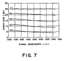
The present inventor used semiconductor LDs with the following oscillation wavelengths: λ1 = 1423.516 nm, λ2 = 1430.990 nm, λ3 = 1438.543 nm, and λ4 = 1460.265 nm, adjusting such that their respective pump intensities are 248.0 mW, 170.0 mW, 128.0 mW, and 264.5 mW as shown in (1) of Table 1. As a result, a flat gain of 25 dB was obtained in the signal band of 1530 to 1560 nm as shown in (1) of Fig. 7.
Thereafter, as shown in (2) through (5) of Table 1, signal band gain was measured with all the pump intensities reduced to 80%, 60%, 40%, and 20% to obtain values as indicated by the solid lines (2) through (5) of the Fig. 7. These solid lines indicate that although flatness of the signal band gain is maintained, the gains at the longer wavelength vary to a somewhat greater as compared with the gains at the shorter wavelength, indicating negative gain tilts.
Shorter wavelength group Longer wavelength group
λ1 λ2 λ3 λ4
(1) 100%
248.0 170.0 128.0 264.5
(2) 80%
199.2 136.0 102.4 211.6
(3) 60%
149.4 102.0 76.8 158.7
(4) 40%
99.6 68.0 51.2 105.8
(5) 20%
49.8 34.0 25.6 52.9
[mW]
Further, while maintaining the pump intensity of the semiconductor LD of 1460.265 nm at 100%, signal band gain was measured with the pump intensity of three shorter wavelengths semiconductor LDs of 1423.516 nm, 1430.990 nm, and 1438.543 nm reduced to 80%, 60%, 40%, and 20%, as shown in (6) through (9) of Table 2. The results are the values indicated by the solid lines (6) through (9) of Fig. 6. In these solid lines, the gain at the shorter wavelength of the signal band varies more greatly than the gain at the longer wavelength, and the gain flatness is sufficient.
Shorter wavelength group Longer wavelength group
λ1 λ2 λ3 λ4
(6) 80% 100%
199.2 136.0 102.4 264.5
(7) 60% 100%
149.4 102.0 76.8 264.5
(8) 40% 100%
99.6 68.0 51.2 264.5
(9) 20% 100%
49.8 34.0 25.6 264.5
(10) 100% 80%
248.0 170.0 128.0 211.6
(11) 100% 60%
248.0 170.0 128.0 158.7
(12) 100% 40%
248.0 170.0 128.0 105.8
(13) 100% 20%
248.0 170.0 128.0 52.9
[mW]
Further, while maintaining the pump intensity of the three shorter wavelengths semiconductor LDs at 100%, the present inventor performed signal band gain measurement with the pump intensity of the semiconductor LD of 1460.265 nm reduced to 80%, 60%, 40%, and 20%, as shown in (10) through (13) of Table 2. The results are the values indicated by the dotted lines (10) through (13) of Fig. 6. In these dotted lines, the gain at the shorter wavelength of the signal band does not vary compared with the gain at the longer wavelength, and the gain flatness is sufficient.
The present inventor divided pumps optimized so as to obtain flat gain properties in a certain signal band into Group A of the shorter wavelength and Group B of the longer wavelength to find out the following:
  • A. When the pump powers of Groups A and B are lowered at the same rate, the Raman gain indicates a decrease with a negative tilt.
  • B. When the pump powers of the Group B are all lowered at the same rate while maintaining the pump power of Group A at 100%, the Raman gain indicate a decrease with a negative gain tilt.
  • C. When the pump powers of the Group A are all lowered at the same rate while maintaining the pump power of Group B at 100%, the Raman gain indicates a decrease with a positive tilt. Further, although not shown, by increasing the pump powers of Groups A and B, the following have been found out:
  • D. When the pump powers of Groups A and B are raised at the same rate, the Raman gain indicates an increase in level with a positive tilt.
  • E. When the pump powers of the Group B are all raised at the same rate while maintaining the pump power of Group A at 100%, the Raman gain indicate an increase with a positive tilt.
  • F. When the pump powers of the Group A are all raised at the same rate while maintaining the pump power of Group B at 100%, the Raman gain indicates an increase with a negative tilt. Further, when optical fibers of different amplification factors are used as shown in (14) through (18) of Table 3, the different gain properties are obtained even if the same pump power is supplied, as shown in Fig. 5. That is, the following facts are ascertained:
  • G. When an optical fiber of a large Raman gain coefficient is used, the Raman gain properties indicate an increase with a positive tilt.
  • H. When an optical fiber of a small Raman gain coefficient is used, the Raman gain properties indicate a decrease with a negative tilt.
    Gain coefficient Rate of change
    (14) 2.045 100%
    (15) 4.090 200%
    (16) 3.272 160%
    (17) 2.454 120%
    (18) 1.636 80%
  • Thus, it has been found out that by combining the above techniques of A through H, it is possible to easily design a Raman amplifier with good gain flatness and having an arbitrary gain level and tilting.
    The present invention has been made in view of the above facts. In accordance with the present invention, pump wavelengths are divided into two groups; the shorter wavelengths and the longer wavelengths, which are arbitrarily adjusted, whereby it is possible to obtain arbitrary gain properties.
    In accordance with the present invention, there is provided a pump light source for outputting a plurality of pump lightwaves for effecting Raman amplification on signal lightwaves input to a light transmission path, wherein: the pump light source for Raman amplification is divided into light source whose oscillation wavelengths are the shorter (hereinafter referred to as "shorter wavelength light source) and light source whose oscillation wavelengths are the longer (hereinafter referred to as "longer wavelength light source); a plurality of lightwaves emitted from the shorter wavelength light source and a lightwave emitted from the longer wavelength light source are coupled and output; and the plurality of lightwaves output from the shorter wavelength light source or the lightwave output from the longer wavelength light source is collectively controlled to adjust the intensity of the output light.
    In accordance with the present invention, there is further provided a Raman amplifier including a light transmitting station for emitting signal lightwaves, a light receiving station for receiving the signal lightwaves, a light transmission path for propagating the signal lightwaves from the light transmitting station to the light receiving station, and a pump light source for Raman amplification which introduces pump lightwaves into the light transmission path to cause Raman scattering in the light transmission path to thereby effect Raman amplification on the signal lightwaves, wherein the pump light source for Raman amplification is as claimed in one of Claims 1 through 5.
    Brief Description of the Drawings
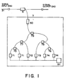
  • Fig. 1 is a schematic diagram showing an embodiment of the present invention;
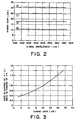
  • Fig. 2 is a Raman gain profile in an embodiment of the present invention;
  • Fig. 3 is a property diagram showing the relationship between the rate of change in pump power at the shorter wavelength group with respect to the rate of change in drive current at the longer wavelength group and the Raman gain;
  • Fig. 4 is a schematic diagram showing another embodiment of the present invention;
  • Fig. 5 is a property diagram showing the relationship between signal wavelength and Raman amplification gain when the gain coefficient of an optical fiber is changed;
  • Fig. 6 is a property diagram showing the relationship between signal wavelength and Raman amplification gain when the pump power supplied to the optical fiber is changed;
  • Fig. 7 is a property diagram showing the relationship between signal wavelength and Raman amplification gain when the pump power supplied to the optical fiber is changed;
  • Fig. 8 is a schematic diagram showing an ordinary Raman amplifier; and
  • Fig. 9 is a schematic diagram showing an ordinary backward pumping type Raman amplification system.
  • Embodiments of the Invention
    Fig. 1 is a schematic diagram showing an embodiment of the present invention. In the drawing, 31, 6, and 7 respectively indicate a Raman amplification medium, such as a silica-based optical fiber, an optical coupler for coupling pump lightwaves with signal lightwaves to be integrated in the Raman amplification medium, and a Raman amplification pump light source. 71·71 indicate semiconductor laser diodes of an oscillation wavelength of 1423.516 nm, 72 indicates a semiconductor laser diode of an oscillation wavelength of 1430.990 nm, 73 indicates a semiconductor laser diode of an oscillation wavelength of 1438.543 nm, and 74·74 indicate semiconductor laser diodes of an oscillation wavelength of 1460.265 nm. 75 and 76 indicate polarization beam combiner, 77, 78, and 79 indicate wavelength optical multiplexers for coupling two lightwaves, and 80 indicates an optical isolator. 81 indicates a current controller capable of supplying drive current to the semiconductor laser diodes 71 through 74 and controlling the current values thereof.
    The lightwaves from the semiconductor laser diodes 71·71 are coupled in the polarization beam combiner 75 such that their states of polarization differ from each other by 90 degrees, and then output. Similarly, the lightwaves from the semiconductor laser diodes 74·74 are coupled in the polarization beam combiner 76 such that their states of polarization differ from each other by 90 degrees, and then output. The lightwaves from the semiconductor laser diodes 71 · 71, coupled by the polarization beam combiner 75, and the lightwave from the semiconductor laser diode 72 are coupled by the wavelength optical multiplexer 77. The lightwaves from the semiconductor laser diodes 74 · 74, coupled by the polarization beam combiner 76, and the lightwave from the semiconductor laser diode 73 are coupled by the wavelength optical multiplexer 78. The lightwaves output from the wavelength optical multiplexers 77 and 78 are coupled by the wavelength optical multiplexer 79, and guided to the Raman amplification medium 31 through the optical coupler 6 and the isolator 80.
    Forty-four input signals in substantially uniform variation between wavelengths of 1527.994 nm and 1562.233 nm are introduced into the Raman amplification medium 31 from the input end in a magnitude of substantially -15 dBm/ch. The semiconductor laser diodes 71·71 are adjusted by the current controller 81 such that optical powers of them are the same each other. Furthermore, the semiconductor laser diodes 74·74 are adjusted by the current controller 81 such that optical powers of them are the same each other.
    In the above condition, the drive current for the semiconductor laser diodes 71 through 74 was adjusted by the current controller 81, an optical spectrum analyzer (not shown) was mounted to the output end, and current adjustment was performed such that the gain was approximately 25 dB and flat over the entire signal band. The light intensities of the semiconductor laser diodes 71 through 74 at this time were respectively 248 mW, 170 mW, 128 mW, and 264.5 mW as shown in (1) of Table 4, (The intensity of light output from each of the semiconductor laser diodes 71 and 74 is 1/2 thereof). At this time, the gain is within the range of 24.74 to 25.30 dB, and is in a substantially flat state as shown in (1) of Fig. 2. In the present invention, this value will be defined as pump power 100% for the sake of convenience.
    Shorter wavelength group Longer wavelength group
    λ1 λ2 λ3 λ4
    (1) 100% 100%
    248.0 170.0 128.0 264.50
    (2) 140% 113%
    348.60 238.00 179.20 343.85
    (3) 60% 84%
    149.40 102.00 76.80 211.60
    (4) 31.2% 60%
    77.688 53.040 39.936 158.700
    [mW]
    Next, similarly, by controlling the semiconductor laser diodes 71 through 74 by the current controller 81, the light intensity of the semiconductor laser diodes 71 through 73 was increased to 140%, and the light intensity of the semiconductor laser diode 74 was increased to 113%, as shown in (2) of Table 4. The respective light intensities of the semiconductor laser diodes 71 through 74 at that time were 348.6 mW, 238 mW, 179.2 mW, and 343.85 mW (The light intensity of the light output from each of the semiconductor laser diodes 71 and 74 is 1/2 thereof). The gain at this time is within the range of 30.01 to 30.77 dB, and is in a substantially flat state as shown in (2) of Fig. 2.
    Next, similarly, by controlling the semiconductor laser diodes 71 through 74 by the current controller 81, the light intensity of the semiconductor laser diodes 71 through 73 was reduced to 60%, and the light intensity of the semiconductor laser diode 74 was reduced to 84%, as shown in (3) of Table 4. The respective light intensities of the semiconductor laser diodes 71 through 74 at that time were 149.4 mW, 102 mW, 76.8 mW, and 211.6 mW (The intensity of the light output from each of the semiconductor laser diodes 71 and 74 is 1/2 thereof). The gain at this time is within the range of 17.36 to 17.76 dB, and is in a substantially flat state, as shown in (3) of Fig. 2.
    Next, in a similar manner, by controlling the semiconductor laser diodes 71 through 74 by the current controller 81, the light intensity of the semiconductor laser diodes 71 through 73 was reduced to 31.2%, and the light intensity of the semiconductor laser diode 74 was reduced to 60%, as shown in (4) of Table 4. The respective light intensities of the semiconductor laser diodes 71 through 74 at that time were 77.688 mW, 53.04 mW, 39.936 mW, and 158.7 mW (The intensity of the light output from each of the semiconductor laser diodes 71 and 74 is 1/2 thereof). The gain at this time is within the range of 10.44 to 10.73 dB, and is in a substantially flat state, as shown in Fig. 2, (4).
    The drive current at the shorter wavelength group and the drive current at the longer wavelength group were collectively controlled to further vary the intensity of the light from each semiconductor laser diode in a manner other than that of the above-mentioned four examples so as to obtain a substantially flat gain over the entire signal wavelength band. Table 5 shows the percentage of the pump power, using the above-mentioned 100% as a reference. Fig. 3 is a graph plotting the measurement values. The vertical axis (Y-axis) indicates the rate of change of the semiconductor laser diodes 71 through 73 with respect to the rate of change of the semiconductor laser diode 74, and the horizontal axis (X-axis) indicates the gain properties.
    This graph is considerably in conformity with the curve according to the following expression: y = 0.0006X2 + 0.0129X + 0.3202
    λ1-3 λ4 Raman gain λ1-3/λ4
    % % dB
    7.2 20.0 2.95 0.360
    17.1 40.0 6.37 0.428
    20.0 45.0 7.30 0.444
    31.2 60.0 10.54 0.520
    40.0 69.0 12.80 0.580
    53.7 80.0 16.13 0.671
    60.0 84.0 17.54 0.714
    80.0 93.6 21.61 0.855
    100.0 100.0 25.00 1.000
    120.0 106.7 28.14 1.125
    140.0 113.0 30.57 1.239
    160.0 120.0 32.55 1.333
    180.0 127.5 34.13 1.412
    Thus, to obtain an arbitrary Raman gain α by using an optical component according to this embodiment, α is substituted in the X of the above equation to obtain the value of Y, and solely by adjusting the light intensities of both wavelength groups while setting the ratio of the light intensity of the shorter wavelength group to the light intensity of the longer wavelength group such that it becomes equal to the above value of Y, it is possible to obtain an arbitrary flat gain property.
    Fig. 4 is a schematic diagram showing another embodiment of the present invention. In the drawing, 82 and 83 indicate optical attenuators, and 84 indicates a controller for controlling the attenuation amount thereof. The other components are the same as those of Fig. 1.
    The lightwaves from the semiconductor laser diodes 71·71 are coupled in the polarization beam combiner 75 such that their states of polarization differ from each other by 90 degrees before being output. Similarly, the lightwaves from the semiconductor laser diodes 74·74 are coupled in the polarization beam combiner 76 such that their states of polarization differ from each other by 90 degrees before being output. The lightwaves from the semiconductor laser diodes 71 · 71, coupled by the polarization beam combiner 75, and the lightwave from the semiconductor laser diode 72 are coupled by the wavelength optical multiplexer 77. The lightwaves from the semiconductor laser diodes 71·71 and 72, coupled by the wavelength optical multiplexer 77, and the lightwave from the semiconductor laser diode 73 are coupled by the wavelength optical multiplexer 78. The lightwaves output from the wavelength optical multiplexer 78 and the polarization beam combiner 76 are attenuated by the optical attenuators 82 and 83, respectively and then coupled by the wavelength optical multiplexer 79 before being guided to the optical coupler 6 through the isolator 80 and then guided to the Raman amplification medium 31.
    The effect achieved in the above state is the same as that of the embodiment shown in Fig. 1.
    In the above-described embodiments, the cases are explained where there are three light sources at the shorter wavelength group and one light source at the longer wavelength group. The present invention may be also applied to other cases where the number of light sources for each group is not the number disclosed above. However, it is always necessary to provide a plurality of light sources for the shorter wavelength group. Needless to say, the light source for each group may include one or more wavelengths.
    While, in the above embodiments, the cases are explained where a flat gain distribution is attained, it is also possible to impart an arbitrary inclination to the gain profile through adjustment of the rate of fluctuation in the drive current of the semiconductor laser diodes at the shorter wavelength group and the drive current at the longer wavelength group.
    Industrial Availability
    As described above, in accordance with the present invention, solely by individually varying the light intensity of the shorter wavelength group and the light intensity of the longer wavelength group, it is advantageously possible to obtain a Raman amplifier having an arbitrary wavelength property superior in flatness and an arbitrary amplification gain. Further, it is possible to obtain a targeted gain with little adjustment.
    Claims (8)

    1. A pump light source for Raman amplification for outputting a plurality of pump lightwaves for effecting Raman amplification on signal lightwaves input to a light transmission path, wherein: the pump light source for Raman amplification is divided into light source whose oscillation wavelength is the shorter wavelength and light source whose oscillation wavelength is the longer wavelength; a plurality of lightwaves emitted from the shorter wavelength light source and one or more lightwave emitted from the longer wavelength light source are coupled and output; and the plurality of lightwaves output from the shorter wavelength light source or the lightwave output from the longer wavelength light source is collectively controlled to adjust the intensity of the output light.
    2. A pump light source for Raman amplification according to Claim 1, wherein: drive currents for a plurality of light sources at the shorter wavelength are collectively controlled to adjust the output light intensity at the shorter wavelength.
    3. A pump light source for Raman amplification according to Claim 1, wherein: lightwaves oscillated from a plurality of light sources whose lightwave is the shorter wavelength are coupled and collectively controlled by a optical attenuator to thereby adjust the output light intensity at the shorter wavelength.
    4. A pump light source for Raman amplification according to any one of Claims 1 through 3, wherein: the intensity of the oscillation light at the shorter wavelength and the intensity of the oscillation light at the longer wavelength are simultaneously adjusted.
    5. A pump light source for Raman amplification according to Claim 4, wherein: the intensity of the oscillation light at the shorter wavelength and the intensity of the oscillation light at the longer wavelength are varied in proportion of 1 to 0.81.
    6. A pump light source for Raman amplification according to Claim 4, wherein: the intensity of the oscillation light at the shorter wavelength and the intensity of the oscillation light at the longer wavelength are varied in proportion of 1 to 1.40.
    7. A pump light source for Raman amplification according to Claim 4, wherein: the intensity of the oscillation light at the shorter wavelength and the intensity of the oscillation light at the longer wavelength are varied in proportion of 1 to 1.92.
    8. Raman amplification device comprising a. light transmitting station for emitting signal lightwaves, a light receiving station for receiving the signal lightwaves, a light transmission path for propagating the signal lightwaves from the light transmitting station to the light receiving station, and a pump light source for Raman amplification which introduces pump lightwaves into the light transmission path to cause Raman scattering in the light transmission path to thereby effect Raman amplification on the signal lightwaves, wherein: the pump light source for Raman amplification is one as claimed in any one of Claims 1 through 7.
    EP02250710A 2001-02-02 2002-02-01 Pump light source for raman amplifier and raman amplifier using the same Withdrawn EP1229675A3 (en)

    Applications Claiming Priority (2)

    Application Number Priority Date Filing Date Title
    JP2001027201 2001-02-02
    JP2001027201 2001-02-02

    Publications (2)

    Publication Number Publication Date
    EP1229675A2 true EP1229675A2 (en) 2002-08-07
    EP1229675A3 EP1229675A3 (en) 2004-09-22

    Family

    ID=18891901

    Family Applications (1)

    Application Number Title Priority Date Filing Date
    EP02250710A Withdrawn EP1229675A3 (en) 2001-02-02 2002-02-01 Pump light source for raman amplifier and raman amplifier using the same

    Country Status (3)

    Country Link
    US (1) US6950230B2 (en)
    EP (1) EP1229675A3 (en)
    CA (1) CA2369766A1 (en)

    Families Citing this family (5)

    * Cited by examiner, † Cited by third party
    Publication number Priority date Publication date Assignee Title
    KR100533914B1 (en) * 2003-10-08 2005-12-06 한국전자통신연구원 Raman amplifier and Raman pumping method
    EP1788728A1 (en) * 2005-11-18 2007-05-23 Alcatel Lucent Raman amplifier and optical transmission system
    JP4750688B2 (en) * 2006-12-27 2011-08-17 富士通株式会社 Raman amplifier
    JP5058855B2 (en) * 2008-03-13 2012-10-24 キヤノン株式会社 Information processing apparatus, method thereof, and program
    US9017334B2 (en) 2009-02-24 2015-04-28 Microport Orthopedics Holdings Inc. Patient specific surgical guide locator and mount

    Family Cites Families (28)

    * Cited by examiner, † Cited by third party
    Publication number Priority date Publication date Assignee Title
    US4616898A (en) 1980-03-31 1986-10-14 Polaroid Corporation Optical communication systems using raman repeaters and components therefor
    JPS56165437A (en) 1980-05-26 1981-12-19 Kokusai Denshin Denwa Co Ltd <Kdd> Optical repeating system for optical communication
    US4699452A (en) 1985-10-28 1987-10-13 American Telephone And Telegraph Company, At&T Bell Laboratories Optical communications system comprising Raman amplification means
    US6191877B1 (en) 1995-02-17 2001-02-20 Lucent Technologies Inc. WDM optical fiber system using Raman amplification
    US5673280A (en) 1996-02-12 1997-09-30 Lucent Technologies Inc. Article comprising low noise optical fiber raman amplifier
    US5959750A (en) 1996-06-06 1999-09-28 Lucent Technologies Inc. Method of upgrading transmission capacity by Raman amplification
    US5946428A (en) 1996-07-09 1999-08-31 Corning Incorporated Fiber optic system with simultaneous switching and raman
    US5966206A (en) 1996-10-10 1999-10-12 Tyco Submarine Systems Ltd. Interlocked high power fiber system using OTDR
    US6212310B1 (en) 1996-10-22 2001-04-03 Sdl, Inc. High power fiber gain media system achieved through power scaling via multiplexing
    US6081323A (en) 1997-02-27 2000-06-27 The United States Of America As Represented By The Director Of The National Security Agency Measurement of Raman gain spectrum in optical fiber
    US6081366A (en) 1997-08-28 2000-06-27 Lucent Technologies Inc. Optical fiber communication system with a distributed Raman amplifier and a remotely pumped er-doped fiber amplifier
    US5887093A (en) 1997-09-12 1999-03-23 Lucent Technologies Incorporated Optical fiber dispersion compensation
    US6038356A (en) 1997-09-25 2000-03-14 Tyco Submarine Systems Ltd. Lightwave transmission system employing raman and rare-earth doped fiber amplification
    WO1999043107A1 (en) 1998-02-20 1999-08-26 Ciena Corporation Optical amplifier having an improved noise figure
    US5966480A (en) 1998-02-23 1999-10-12 Lucent Technologies Inc. Article comprising an improved cascaded optical fiber Raman device
    US6320884B1 (en) 1998-02-26 2001-11-20 Tycom (Us) Inc., Wide bandwidth Raman amplifier employing a pump unit generating a plurality of wavelengths
    JP4094126B2 (en) 1998-07-09 2008-06-04 富士通株式会社 Rare earth doped optical fiber and optical fiber amplifier using the same
    US6115174A (en) 1998-07-21 2000-09-05 Corvis Corporation Optical signal varying devices
    US6344922B1 (en) * 1998-07-21 2002-02-05 Corvis Corporation Optical signal varying devices
    EP2306605B1 (en) * 1998-07-23 2012-05-23 The Furukawa Electric Co., Ltd. Pumping unit for a Raman amplifier and Raman amplifier comprising the same
    JP2000151507A (en) 1998-11-09 2000-05-30 Nippon Telegr & Teleph Corp <Ntt> Optical transmission system
    US6181464B1 (en) 1998-12-01 2001-01-30 Tycom (Us) Inc. Low noise Raman amplifier employing bidirectional pumping and an optical transmission system incorporating same
    JP4100797B2 (en) 1999-01-14 2008-06-11 古河電気工業株式会社 Optical amplifier
    US6163636A (en) 1999-01-19 2000-12-19 Lucent Technologies Inc. Optical communication system using multiple-order Raman amplifiers
    US6147794A (en) 1999-02-04 2000-11-14 Lucent Technologies, Inc. Raman amplifier with pump source for improved performance
    US6052219A (en) 1999-02-16 2000-04-18 Tyco Submarine Systems Ltd. Wide bandwidth Raman amplifier capable of employing pump energy spectrally overlapping the signal
    JP4821037B2 (en) * 2000-08-25 2011-11-24 富士通株式会社 Optical amplifier and Raman pump light source using Raman amplification
    JP2002076482A (en) * 2000-08-31 2002-03-15 Fujitsu Ltd Optical amplifier, optical amplification method, and optical amplification system

    Also Published As

    Publication number Publication date
    CA2369766A1 (en) 2002-08-02
    US20020159133A1 (en) 2002-10-31
    US6950230B2 (en) 2005-09-27
    EP1229675A3 (en) 2004-09-22

    Similar Documents

    Publication Publication Date Title
    KR100417322B1 (en) Optical amplifier and a method of controlling the optical amplifier
    US6728026B2 (en) Dynamically tunable optical amplifier and fiber optic light source
    US20020060837A1 (en) Gain and signal level adjustments of cascaded optical amplifiers
    JP3757018B2 (en) Optical amplification device, optical amplification device control method, and optical transmission system using optical amplification device
    EP1036440A1 (en) Optical amplifier having an improved noise figure
    JP2002504756A (en) Upgradeable gain-flattened fiber amplifier for WDM processing
    RU2202151C2 (en) Pump oscillator wavelength adjustment for optical amplifiers and its use in wavelength- division multiplex systems
    KR20020008772A (en) Raman amplifier
    EP1037337B1 (en) Optical amplifier
    JP2000269578A (en) Method, apparatus and system for optical amplification
    US7158285B2 (en) Raman amplification repeater and optical transmission system using the same
    US6683713B2 (en) Method, device, and system for level equalization
    JP2001024594A (en) Optical amplifier and system having the optical amplifier
    US6950230B2 (en) Pump light source for Raman amplifier and Raman amplifier using the same
    KR20040005698A (en) Light amplification module, light amplifier and optical communication system
    JP3949463B2 (en) Excitation light source for Raman amplifier and Raman amplifier using the same
    JP2004301991A (en) Optical amplification control unit and optical amplification control method
    KR100567317B1 (en) Optical fiber amplification method and apparatus for controlling gain
    US7042632B2 (en) Raman amplifier
    US6687043B2 (en) Multi-frequency Raman amplifier pump source
    JP3961266B2 (en) Optical amplifier
    JP4108459B2 (en) Optical amplifier
    KR100367085B1 (en) Device for Compensation of Loss Variation in Optical Transmission Line
    KR20030089278A (en) Multi-Stage Erbium Doped Amplifier for Wavelength Division Multiplexing System
    JPH08250785A (en) Optical amplification repeater

    Legal Events

    Date Code Title Description
    PUAI Public reference made under article 153(3) epc to a published international application that has entered the european phase

    Free format text: ORIGINAL CODE: 0009012

    AK Designated contracting states

    Kind code of ref document: A2

    Designated state(s): AT BE CH CY DE DK ES FI FR GB GR IE IT LI LU MC NL PT SE TR

    AX Request for extension of the european patent

    Free format text: AL;LT;LV;MK;RO;SI

    PUAL Search report despatched

    Free format text: ORIGINAL CODE: 0009013

    AK Designated contracting states

    Kind code of ref document: A3

    Designated state(s): AT BE CH CY DE DK ES FI FR GB GR IE IT LI LU MC NL PT SE TR

    AX Request for extension of the european patent

    Extension state: AL LT LV MK RO SI

    AKX Designation fees paid

    Designated state(s): DE FR GB IT

    STAA Information on the status of an ep patent application or granted ep patent

    Free format text: STATUS: THE APPLICATION IS DEEMED TO BE WITHDRAWN

    18D Application deemed to be withdrawn

    Effective date: 20050323