EP1229641A1 - Self oscillating power amplifier - Google Patents
Self oscillating power amplifier Download PDFInfo
- Publication number
- EP1229641A1 EP1229641A1 EP01400257A EP01400257A EP1229641A1 EP 1229641 A1 EP1229641 A1 EP 1229641A1 EP 01400257 A EP01400257 A EP 01400257A EP 01400257 A EP01400257 A EP 01400257A EP 1229641 A1 EP1229641 A1 EP 1229641A1
- Authority
- EP
- European Patent Office
- Prior art keywords
- coupled
- amplifier arrangement
- differential
- power amplifier
- self
- Prior art date
- Legal status (The legal status is an assumption and is not a legal conclusion. Google has not performed a legal analysis and makes no representation as to the accuracy of the status listed.)
- Granted
Links
- 230000008878 coupling Effects 0.000 claims abstract description 11
- 238000010168 coupling process Methods 0.000 claims abstract description 11
- 238000005859 coupling reaction Methods 0.000 claims abstract description 11
- 239000003990 capacitor Substances 0.000 claims description 9
- 238000004804 winding Methods 0.000 claims description 4
- 230000010355 oscillation Effects 0.000 abstract description 15
- 238000005516 engineering process Methods 0.000 description 4
- 230000001419 dependent effect Effects 0.000 description 3
- 101100033865 Saccharomyces cerevisiae (strain ATCC 204508 / S288c) RFA1 gene Proteins 0.000 description 2
- 101100524516 Saccharomyces cerevisiae (strain ATCC 204508 / S288c) RFA2 gene Proteins 0.000 description 2
- 230000003247 decreasing effect Effects 0.000 description 2
- 230000000694 effects Effects 0.000 description 2
- 230000036039 immunity Effects 0.000 description 2
- 238000001228 spectrum Methods 0.000 description 2
- 239000010752 BS 2869 Class D Substances 0.000 description 1
- 230000003139 buffering effect Effects 0.000 description 1
- 230000008030 elimination Effects 0.000 description 1
- 238000003379 elimination reaction Methods 0.000 description 1
- 238000001914 filtration Methods 0.000 description 1
- 230000001939 inductive effect Effects 0.000 description 1
- 238000002955 isolation Methods 0.000 description 1
- 238000005070 sampling Methods 0.000 description 1
- 230000001629 suppression Effects 0.000 description 1
Images


Classifications
-
- H—ELECTRICITY
- H03—ELECTRONIC CIRCUITRY
- H03F—AMPLIFIERS
- H03F3/00—Amplifiers with only discharge tubes or only semiconductor devices as amplifying elements
- H03F3/20—Power amplifiers, e.g. Class B amplifiers, Class C amplifiers
- H03F3/21—Power amplifiers, e.g. Class B amplifiers, Class C amplifiers with semiconductor devices only
- H03F3/217—Class D power amplifiers; Switching amplifiers
- H03F3/2173—Class D power amplifiers; Switching amplifiers of the bridge type
-
- H—ELECTRICITY
- H03—ELECTRONIC CIRCUITRY
- H03F—AMPLIFIERS
- H03F1/00—Details of amplifiers with only discharge tubes, only semiconductor devices or only unspecified devices as amplifying elements
- H03F1/02—Modifications of amplifiers to raise the efficiency, e.g. gliding Class A stages, use of an auxiliary oscillation
- H03F1/0205—Modifications of amplifiers to raise the efficiency, e.g. gliding Class A stages, use of an auxiliary oscillation in transistor amplifiers
-
- H—ELECTRICITY
- H03—ELECTRONIC CIRCUITRY
- H03F—AMPLIFIERS
- H03F3/00—Amplifiers with only discharge tubes or only semiconductor devices as amplifying elements
- H03F3/45—Differential amplifiers
- H03F3/45071—Differential amplifiers with semiconductor devices only
- H03F3/45076—Differential amplifiers with semiconductor devices only characterised by the way of implementation of the active amplifying circuit in the differential amplifier
- H03F3/45179—Differential amplifiers with semiconductor devices only characterised by the way of implementation of the active amplifying circuit in the differential amplifier using MOSFET transistors as the active amplifying circuit
-
- H—ELECTRICITY
- H03—ELECTRONIC CIRCUITRY
- H03F—AMPLIFIERS
- H03F2200/00—Indexing scheme relating to amplifiers
- H03F2200/537—A transformer being used as coupling element between two amplifying stages
-
- H—ELECTRICITY
- H03—ELECTRONIC CIRCUITRY
- H03F—AMPLIFIERS
- H03F2200/00—Indexing scheme relating to amplifiers
- H03F2200/541—Transformer coupled at the output of an amplifier
Definitions
- the present invention relates to a power amplifier as is described in the non-characterising portion of the first claim.
- a power amplifier is already known in the art, e.g. from the article " An IC for Linearizing RF Power Amplifiers using Envelope Elimination and Restoration", by D. Su and W. McFarland, ISSCC 1998 Technical Digest, paper 3.6-2.
- a circuit is shown wherein a comparator in series with a Class-D buffer and a lowpass filter is coupled to a resistive load, this circuit having a direct feedback from the output to the input of the system.
- An object of the present invention is to provide a power amplifier of the above known type but which has a much better power efficiency compared to the prior art circuit.
- this object is achieved due to the presence of a low-pass filter in the feedback loop of the amplifier arrangement, as is further described in the characterising portion of the first claim.
- this amplifier is a switching type amplifier a high efficiency can be obtained, even when buffering signals with a high crest factor as in xDSL. Since, in comparison to the prior art system no clock is used, power efficiency is seriously improved.
- the minimum self-oscillation frequency which is mainly determined by the cut-off frequency of the low pass filter in the feedback path, merely has to be a factor 3 larger than the bandwidth of the input signal to be amplified.
- the switching or clock frequency has to be generally more than a factor 10 larger than the bandwidth of the input signal to obtain enough suppression of the quantisation noise. This is because in the prior art system the signal is presented by a discrete amplitude, discrete time signal while in the present amplifier it is a discrete amplitude, continuous time signal. This presents an additional advantage of the present amplifier with respect to higher obtainable bandwidths.
- Claim 4 describes the differential version of the output amplifier arrangement.
- the differential structure Compared to the single-ended version, the differential structure provides power supply modulation rejection and better noise immunity. This adds to the maximum Signal to Noise ratio attainable in the present amplifier.
- the high frequency common mode component can completely filtered out, and the load is galvanically decoupled from the amplifier.
- the presence of the capacitor improves the coupling between the two oscillation loops and leads to a better signal integrity. Furthermore the combination of this capacitor and the transformer will result in a lowering of the series impedance of the windings of the transformer coils, again improving the efficiency of the amplifier.
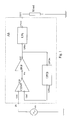
- FIG. 1 A single ended schematic of an output amplifier arrangement AS of the present invention is shown in Fig. 1.
- This amplifier arrangement includes an input terminal IN to which an input signal vin can be supplied.
- the input terminal IN is coupled to a first input terminal Cin1 of a comparator COMP.
- This comparator has a second input terminal Cin2, and is further adapted to compare input signals supplied to both input terminals with each other.
- the result of this comparision is delivered to the output terminal Cout of the comparator, which is further coupled to the input terminal Bin of a digital buffer BUF.
- the latter amplifies the digital input signal present at Bin , for delivery of the amplified signal at its output terminal Bout, which is further coupled to the output terminal OUT of the output amplifier arrangement AS.
- Bout is also coupled in a feedback loop to the second input terminal Cin2 of the comparator, via a feedback low-pass filter LPFB.
- Bout is thus coupled to input terminal LPFBin of LPFB, whereas an output terminal LPFBout of this low-pass filter is coupled to Cin2.
- the amplifier arrangement AS will deliver power to a load RLOAD, via the coupling of the output terminal OUT of the amplifier arrangement AS to a terminal of this load impedance.
- a second low-pass filter LPS is shown in between the buffer output terminal Bout and the output terminal OUT of the amplifier arrangement. The functionality of the amplifier arrangement AS will however first be explained for an embodiment without this second low-pass filter LPS.
- the feedback low-pass loop filter LPFB is constructed in such a way that the loop is unstable , also in the presence of an input signal. This is realised by carefully choosing the cut-off frequency and the order of the low-pass filter such that the self-oscillation frequency, which is the frequency at which the system oscillates without an external input signal present, is at least 3 times larger than the bandwidth of the input frequency of the system. This consideration can for instance be found within tutorial handbook "Multiple-input describing functions and non-linear system design" , written by A. Gelb and W. Vander Velde, Mc-Graw-Hill Book Company, 1968. In this case, the unstability is also preserved in the presence of an input signal .
- the loop will also oscillate, with this self-oscillation frequency, hereafter called the limit cycle frequency , in the presence of an input signal vin.
- the limit or oscillation cycle acts as dither and linearizes the system as long as the error signal between the two inputs of the comparator COMP is smaller than the limit cycle amplitude at the comparator input .
- the output is a square wave containing the limit cycle frequency and the driving input signal.
- limit cycle amplitude is meant the amplitude between the inputs of the comparator in the case of no external input signal present.
- a second low-pass filter can be coupled in between the buffer output terminal Bout and the output terminal OUT of the amplifier arrangement.
- the transfer function of the linearized system is dependent on the limit cycle amplitude.
- the system consisting of the comparator COMP, the buffer BUF and the feedback filter LPFB, can be analyzed by making use of the describing functions approach.
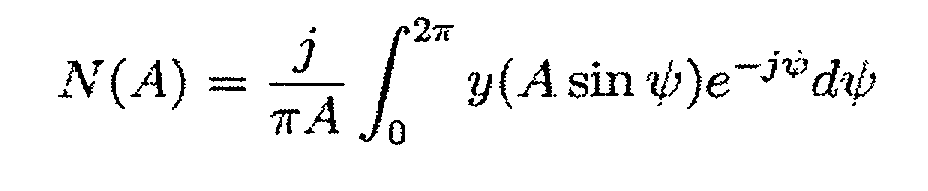
- the comparator COMP followed by the digital buffer BUF can be modeled by the following describing function N'(A).
- N '( A ) N ( A ) p 1 s + p 1
- p1 is the first order pole of the comparator and N(A) is a complex gain, dependent on the input amplitude A.
- This complex amplitude can be calculated as follows : with F(y(x)) being the Fourier Transform of the DC transfer characteristic y(x) of the comparator.
- J0 is the Bessel function of the first kind of order 0.
- J1 is the Bessel function of the first kind of order 1.
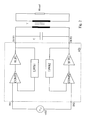
- Fig. 2 shows the differential version of the amplifier arrangement of the present invention.
- This embodiment mainly consists of two similar loops as described in the first embodiment : a first loop consisting of comparator COMP1, digital buffer BUF1 and low-pass filter LPFB1, and a second loop consisting of comparator COMP2, digital buffer BUF2 and low-pass filter LPFB2.
- the first loop is coupled to a first differential input terminal IN1 of the differential amplifier arrangement AD
- the second loop is coupled to a second differential input terminal IN2 of the differential amplifier arrangement AD.
- a differential input signal vdiff can be applied.
- the differential power amplifier arrangement AD includes a pair of differential output terminals : OUT1 and OUT2, to which the two terminals of the load impedance RLOAD can be coupled. Both loops contain similar components such that the limit cycle oscillation frequencies of both loops are the same
- this differential version AD is similar to the operation of the single-ended version AS, in the sense that both individual loops will oscillate at the same limit cycle oscillation frequency. Also in this case the bandwidth of the input signal has to be at least a factor 3 smaller than the self-oscillation frequency of the loops.
- the oscillators are attracted towards each other, forcing the limit cycles to oscillate in phase. Therefore merely the amplified input signal is transferred to the load, while the high frequency oscillation is withheld from this load.
- the differential structure thus provides power supply modulation rejection . Since the limit cycle frequency is not transferred to the load, there is no need to add an additional low-pass filter in series, as was the case for the single-ended embodiment of fig. 1.
- a capacitor C can also be coupled between the two differential output terminals, as is also shown in Fig. 2.
- a capacitor has the advantage of providing a low impedance, which facilitates the attraction between the two loops. In combination with the aforementioned transformator T this capacitor will reduce the high inherent impedance of the transformator.
- Fig. 3 shows detailed embodiments at transistor level of the different components of Figs 1 and 2 .
- the loop filters LPFB, LPFB1 and LPFB2 have been realised as a third order RC filter, denoted “feedback filter” on fig. 3, for keeping a high linearity in the feedback circuitry.
- feedback filter a third order RC filter
- To reduce the transfer time through the comparator a 3-stage structure has been chosen for COMP, COMP1 and COMP2, using positive feedback to ensure a rapid comparison followed by a self-biasing post amplifier. This is all contained in the block denoted “Comparator” in Fig. 3.
- To prevent large shoot-through currents during switching a non-overlapping switching circuit was added. The delay of this non-overlapping signal scheme is combined with a digital buffer to reduce the rise time of the large output driver.
- the transistors contained in the block denoted "digital buffer combined with no DC current circuit” together with those in the block “output driver” all form together an embodiment of the digital buffer B
- this amplifier can be realised using CMOS technologies.
- the circuits of Fig. 3 implemented in a 0.35 ⁇ m CMOS technology, an standard transformer T and a standard coupling capacitor C, were used.
- This complete circuit has been proven feasible to drive any load down to 2.4 Ohm. This is important with respect to the scaling of technology. Indeed, when used as DSL output amplifier, the signal levels on the line tend to remain the same magnitude (15 V), while the supply voltage drops with every technology generation. Transformers are used to overcome this problem and to make a galvanic isolation. Yet the resistance is then decreased by the square of the transformer ratio.
- Fig. 4 shows the output spectrum up to 20 MHz, of the thus realised differential amplifier structure with transformer and coupling capacitor.
- An input signal of 200 kHz was applied.
- the self-oscillation frequency was equal to 3.8 MHz . From this figure it is clear that due to the coupling of both loops the self-oscillation frequency and its harmonics are suppressed. This figure hardly changes for higher signal frequencies up to about 1MHz.
- SFDR For a 800 KHz input signal a 54.4 dB spurious free dynamic range, abbreviated with SFDR is measured.
- the SFDR has decreased to a level of 51.2 dB.
- the linearizing effect drops drastically, since in that case the condition stating that the bandwidth of the input signal has to be at least three times smaller than the self-oscillating frequency, is no longer fulfilled.
Landscapes
- Engineering & Computer Science (AREA)
- Power Engineering (AREA)
- Amplifiers (AREA)
Abstract
Description
The system consisting of the comparator COMP, the buffer BUF and the feedback filter LPFB, can be analyzed by making use of the describing functions approach. In this approach the comparator COMP followed by the digital buffer BUF can be modeled by the following describing function N'(A).


Claims (8)
- Power Amplifier arrangement (AS) including an input terminal (IN) for coupling to an input signal (vin) source, said amplifier arrangement further including a comparator (COMP), a first input terminal (Cin) of which is coupled to said input terminal (IN) of said amplifier arrangement, an output terminal (Cout) of which is coupled to an input terminal (Bin) of a digital buffer (BUF) of said amplifier arrangement, a buffer output terminal (Bout) of said digital buffer being coupled to an output terminal (OUT) of said amplifier arrangement (AS) and to a second input terminal (Cin2) of said comparator (COMP)
characterized in that
said buffer output terminal (BOUT) is coupled via a feedback low-pass filter (LPFB) of said amplifier arrangement (AS), to said second input terminal (Cin2) of said comparator (COMP). - Power amplifier arrangement (AS) according to claim 1
characterized in that
said buffer output terminal (Bout) is coupled to said output terminal (OUT) via a second low-pass filter (LPS) of said amplifier arrangement (AS). - Power amplifier arrangement (AS) according to claim 1
characterized in that
the bandwidth of said input signal (vin) is at least three times smaller than the self-oscillating frequency of said power amplifier arrangement. - Differential power amplifier arrangement (AD) including a pair of differential input terminals (IN1,IN2) to which a differential input voltage (vdiff) can be applied, and a pair of differential output terminal (OUT1,OUT2) for coupling to a load (Rload)said differential power amplifier arrangement including a first self-oscillating loop with an input terminal coupled to a first one (IN1) of said pair of differential input terminals, said first self-oscillating loop including a first comparator (COMP1) coupled to a first digital buffer (BUF1), an output terminal of which is coupled to a second input terminal of said first comparator via a first low-pass filter (LPFB1),said differential power amplifier arrangement incuding a second self- oscillating loop with an input terminal coupled to a second one (IN2) of said pair of differential input terminals, said second self-oscillating loop including a second comparator (COMP2) coupled to a second digital buffer (BUF2), an output terminal of which is coupled to a second input terminal of said second comparator via a second low-pass filter (LPFB2).
- Differential power amplifier arrangement (AD) according to claim 4
characterized in that
said first self-oscillating loop is substantially identical to said second self-oscillating loop. - Differential power amplifier arrangement (AD) according to claim 5
characterized in that
the bandwidth of said differential input signal (vdiff) is at least three times smaller than the self-oscillating frequency of said differential power amplifier arrangement (AD). - Differential power amplifier arrangement (AD) according to claim 4,
characterized in that
said load is coupled to said pair of differential output terminals via a transformer, a primary winding of which is coupled between said pair of differential output terminals (OUT1, OUT2), a secondary winding of which is coupled in parallel to said load. - Differential power amplifier arrangement (AD) according to claims 4 or 7
characterised in that
said load is coupled in parallel with a capacitor (C), which is coupled between said pair of differential output terminals (OUT1,OUT2).
Priority Applications (4)
| Application Number | Priority Date | Filing Date | Title |
|---|---|---|---|
| EP01400257.0A EP1229641B1 (en) | 2001-02-01 | 2001-02-01 | Self oscillating power amplifier |
| JP2002017922A JP2002290158A (en) | 2001-02-01 | 2002-01-28 | Self-excited oscillation power amplifier |
| US10/059,439 US6861902B2 (en) | 2001-02-01 | 2002-01-31 | Self oscillating power amplifier |
| CN02103162.2A CN1288836C (en) | 2001-02-01 | 2002-02-01 | Self-oscillation powre amplifier |
Applications Claiming Priority (1)
| Application Number | Priority Date | Filing Date | Title |
|---|---|---|---|
| EP01400257.0A EP1229641B1 (en) | 2001-02-01 | 2001-02-01 | Self oscillating power amplifier |
Publications (2)
| Publication Number | Publication Date |
|---|---|
| EP1229641A1 true EP1229641A1 (en) | 2002-08-07 |
| EP1229641B1 EP1229641B1 (en) | 2013-11-06 |
Family
ID=8182613
Family Applications (1)
| Application Number | Title | Priority Date | Filing Date |
|---|---|---|---|
| EP01400257.0A Expired - Lifetime EP1229641B1 (en) | 2001-02-01 | 2001-02-01 | Self oscillating power amplifier |
Country Status (4)
| Country | Link |
|---|---|
| US (1) | US6861902B2 (en) |
| EP (1) | EP1229641B1 (en) |
| JP (1) | JP2002290158A (en) |
| CN (1) | CN1288836C (en) |
Cited By (8)
| Publication number | Priority date | Publication date | Assignee | Title |
|---|---|---|---|---|
| DE10233391C1 (en) * | 2002-07-23 | 2003-12-11 | Infineon Technologies Ag | Analogue/digital converter circuit has output of comparator in first A/D converter combined with signal from second A/D converter for residual error correction before low-pass filtering |
| EP1560408A1 (en) * | 2004-01-27 | 2005-08-03 | Infineon Technologies AG | xDSL-line-interface-circuit |
| EP1560412A1 (en) * | 2004-01-27 | 2005-08-03 | Infineon Technologies AG | xDSL-Line-Interface-Circuit |
| EP1594225A1 (en) | 2004-05-05 | 2005-11-09 | Monolithic Power Systems, Inc. | Method and apparatus for self-oscillating differential feedback class-D amplifier |
| US7042284B2 (en) | 2002-09-20 | 2006-05-09 | Alcatel | Operational amplifier arrangement |
| US7535393B1 (en) | 2007-10-24 | 2009-05-19 | Infineon Technologies Ag | Sampling error reduction in PWM-MASH converters |
| US7659842B2 (en) | 2007-10-24 | 2010-02-09 | Infineon Technologies Ag | Quantization error reduction in PWM full-MASH converters |
| US7746256B2 (en) | 2007-10-05 | 2010-06-29 | Infineon Technologies Ag | Analog to digital conversion using irregular sampling |
Families Citing this family (6)
| Publication number | Priority date | Publication date | Assignee | Title |
|---|---|---|---|---|
| US7383500B2 (en) * | 2004-04-30 | 2008-06-03 | Microsoft Corporation | Methods and systems for building packages that contain pre-paginated documents |
| DE102004025437B4 (en) * | 2004-05-24 | 2007-04-05 | Ordin Wladimir | Self-oscillating D-class amplifier with frequency divider |
| EP2221964B1 (en) * | 2009-02-18 | 2015-06-24 | Hypex Electronics B.V. | Self oscillating class D amplification device |
| KR101153552B1 (en) | 2010-12-07 | 2012-06-12 | 한국과학기술원 | Linear amplifier |
| US9143100B2 (en) * | 2013-09-30 | 2015-09-22 | Texas Instruments Incorporated | Method and circuitry for multi-stage amplification |
| DE102022118419A1 (en) | 2022-07-22 | 2024-01-25 | Robert Bosch Gmbh | Tracking amplifier for inductive loads |
Citations (2)
| Publication number | Priority date | Publication date | Assignee | Title |
|---|---|---|---|---|
| US4117415A (en) | 1977-04-14 | 1978-09-26 | Rca Corporation | Bridge amplifiers employing complementary transistors |
| WO1998019391A2 (en) | 1996-10-31 | 1998-05-07 | Bang & Olufsen A/S | Pulse modulation power amplifier with enhanced cascade control method |
Family Cites Families (4)
| Publication number | Priority date | Publication date | Assignee | Title |
|---|---|---|---|---|
| NL8203428A (en) * | 1982-09-02 | 1984-04-02 | Philips Nv | DEVICE FOR CONVERTING AN ELECTRIC SIGNAL TO AN ACOUSTIC SIGNAL. |
| JPH07272186A (en) * | 1994-03-29 | 1995-10-20 | Yokogawa Electric Corp | Process input device |
| DE69829852T2 (en) * | 1998-11-13 | 2006-03-02 | Stmicroelectronics S.R.L., Agrate Brianza | Pulse-width modulated bridge amplifier with configurable input network for analog or digital input without the use of a triangular wave generator |
| US6753729B2 (en) * | 2000-01-06 | 2004-06-22 | Mitek Corporation | Self-oscillating variable frequency closed loop Class D amplifier |
-
2001
- 2001-02-01 EP EP01400257.0A patent/EP1229641B1/en not_active Expired - Lifetime
-
2002
- 2002-01-28 JP JP2002017922A patent/JP2002290158A/en not_active Withdrawn
- 2002-01-31 US US10/059,439 patent/US6861902B2/en not_active Expired - Lifetime
- 2002-02-01 CN CN02103162.2A patent/CN1288836C/en not_active Expired - Lifetime
Patent Citations (2)
| Publication number | Priority date | Publication date | Assignee | Title |
|---|---|---|---|---|
| US4117415A (en) | 1977-04-14 | 1978-09-26 | Rca Corporation | Bridge amplifiers employing complementary transistors |
| WO1998019391A2 (en) | 1996-10-31 | 1998-05-07 | Bang & Olufsen A/S | Pulse modulation power amplifier with enhanced cascade control method |
Non-Patent Citations (4)
| Title |
|---|
| A. GELB; W. VANDER VELDE: "Multiple-input describing functions and non-linear system design", 1968, MC-GRAW-HILL BOOK COMPANY |
| D. SU W. MCFARLAND: "An IC for linearizing RF power amplifiers using envelope elimination and restoration", IEEE INTERNATIONAL SOLID STATE CIRCUITS CONFERENCE., 5 February 1998 (1998-02-05) - 7 February 1998 (1998-02-07), IEEE INC. NEW YORK., US, pages 3.6-1 - 3.6-9, XP002169050, ISSN: 0193-6530 * |
| J.D. SHERMAN: "EDN Electrical Design News", vol. 40, 25 May 1995, CAHNERS PUBLISHING CO., article "Class D amplifiers provide high efficiency for audio systems" |
| SHERMAN J D: "CLASS D AMPLIFIERS PROVIDE HIGH EFFICIENCY FOR AUDIO SYSTEMS", EDN ELECTRICAL DESIGN NEWS,US,CAHNERS PUBLISHING CO. NEWTON, MASSACHUSETTS, vol. 40, no. 11, 25 May 1995 (1995-05-25), pages 103 - 106,108,11, XP000520335, ISSN: 0012-7515 * |
Cited By (13)
| Publication number | Priority date | Publication date | Assignee | Title |
|---|---|---|---|---|
| DE10233391C1 (en) * | 2002-07-23 | 2003-12-11 | Infineon Technologies Ag | Analogue/digital converter circuit has output of comparator in first A/D converter combined with signal from second A/D converter for residual error correction before low-pass filtering |
| US7042284B2 (en) | 2002-09-20 | 2006-05-09 | Alcatel | Operational amplifier arrangement |
| EP1560408A1 (en) * | 2004-01-27 | 2005-08-03 | Infineon Technologies AG | xDSL-line-interface-circuit |
| EP1560412A1 (en) * | 2004-01-27 | 2005-08-03 | Infineon Technologies AG | xDSL-Line-Interface-Circuit |
| US7801296B2 (en) | 2004-01-27 | 2010-09-21 | Infineon Technologies Ag | xDSL-line-interface-circuit |
| CN1694356B (en) * | 2004-05-05 | 2011-01-26 | 美国芯源系统股份有限公司 | Method and apparatus for self-oscillating differential feedback class-D amplifier |
| EP1594225A1 (en) | 2004-05-05 | 2005-11-09 | Monolithic Power Systems, Inc. | Method and apparatus for self-oscillating differential feedback class-D amplifier |
| US8111180B2 (en) | 2007-10-05 | 2012-02-07 | Infineon Technologies Ag | Analog to digital conversion using irregular sampling |
| US7746256B2 (en) | 2007-10-05 | 2010-06-29 | Infineon Technologies Ag | Analog to digital conversion using irregular sampling |
| US7659842B2 (en) | 2007-10-24 | 2010-02-09 | Infineon Technologies Ag | Quantization error reduction in PWM full-MASH converters |
| US7868802B2 (en) | 2007-10-24 | 2011-01-11 | Infineon Technologies Ag | Quantization error reduction in PWM full-MASH converters |
| US7834789B2 (en) | 2007-10-24 | 2010-11-16 | Infineon Technologies Ag | Sampling error reduction in PWM-MASH converters |
| US7535393B1 (en) | 2007-10-24 | 2009-05-19 | Infineon Technologies Ag | Sampling error reduction in PWM-MASH converters |
Also Published As
| Publication number | Publication date |
|---|---|
| JP2002290158A (en) | 2002-10-04 |
| EP1229641B1 (en) | 2013-11-06 |
| CN1288836C (en) | 2006-12-06 |
| US20020171480A1 (en) | 2002-11-21 |
| CN1375927A (en) | 2002-10-23 |
| US6861902B2 (en) | 2005-03-01 |
Similar Documents
| Publication | Publication Date | Title |
|---|---|---|
| US7750731B2 (en) | PWM loop filter with minimum aliasing error | |
| US7301490B2 (en) | Sigma-delta modulated power supply | |
| US6861902B2 (en) | Self oscillating power amplifier | |
| KR100600507B1 (en) | Pulse-width modulation circuit | |
| TW499792B (en) | Power efficient line driver | |
| CN102067444A (en) | Improved filter for switched mode power supply | |
| CN101141114A (en) | CMOS adaptive bias circuit | |
| US7994853B2 (en) | Class-D amplifier with dual feedback loop | |
| WO2009101486A1 (en) | Sigma-delta modulator apparatus and method of generating a modulated output signal | |
| Kang et al. | A review of audio Class D amplifiers | |
| CN1835393B (en) | High-efficiency and high-power audio amplifier and its control method | |
| CN101150303B (en) | Multiple order low pass filter for an xDSL splitter in a telecommunication system | |
| CN110011624B (en) | High-integration composite type audio power amplifying circuit structure | |
| JPH07231226A (en) | Class D power amplifier | |
| CN1694356B (en) | Method and apparatus for self-oscillating differential feedback class-D amplifier | |
| Karmakar et al. | A− 91 dB THD+ N, Class-D Piezoelectric Speaker Driver Using Dual Voltage/Current Feedback for Resistor-Less LC Resonance Damping | |
| CN101356736A (en) | Variable passive component with high resolution value selection and control | |
| US6275102B1 (en) | Distortion correction loop for amplifier circuits | |
| US5796302A (en) | Single pole negative feedback for class-D amplifier | |
| US11837999B2 (en) | Audio amplifier having idle mode | |
| TWI353720B (en) | ||
| WO2022256180A1 (en) | Minimizing total harmonic distortion and power supply induced intermodulation distortion in a single-ended class-d pulse width modulation amplifier | |
| US7388431B2 (en) | Switching amplifier and control method thereof | |
| EP4702669A1 (en) | Zero-common-mode modulation with digital feedback to damp common-mode resonance and suppress cross-over distortion | |
| CN201440647U (en) | Class D amplifier with dual modulation modules |
Legal Events
| Date | Code | Title | Description |
|---|---|---|---|
| PUAI | Public reference made under article 153(3) epc to a published international application that has entered the european phase |
Free format text: ORIGINAL CODE: 0009012 |
|
| AK | Designated contracting states |
Kind code of ref document: A1 Designated state(s): AT BE CH CY DE DK ES FI FR GB GR IE IT LI LU MC NL PT SE TR |
|
| AX | Request for extension of the european patent |
Free format text: AL;LT;LV;MK;RO;SI |
|
| 17P | Request for examination filed |
Effective date: 20030207 |
|
| AKX | Designation fees paid |
Designated state(s): AT BE CH CY DE DK ES FI FR GB GR IE IT LI LU MC NL PT SE TR |
|
| 17Q | First examination report despatched |
Effective date: 20030513 |
|
| RAP1 | Party data changed (applicant data changed or rights of an application transferred) |
Owner name: K.U. LEUVEN RESEARCH & DEVELOPMENT Owner name: ALCATEL LUCENT |
|
| RAP1 | Party data changed (applicant data changed or rights of an application transferred) |
Owner name: K.U. LEUVEN RESEARCH & DEVELOPMENT Owner name: ALCATEL LUCENT |
|
| GRAP | Despatch of communication of intention to grant a patent |
Free format text: ORIGINAL CODE: EPIDOSNIGR1 |
|
| RIC1 | Information provided on ipc code assigned before grant |
Ipc: H03F 3/45 20060101ALI20130521BHEP Ipc: H03F 1/02 20060101ALI20130521BHEP Ipc: H03F 3/217 20060101AFI20130521BHEP |
|
| INTG | Intention to grant announced |
Effective date: 20130610 |
|
| 111Z | Information provided on other rights and legal means of execution |
Free format text: AT BE CH CY DE DK ES FI FR GB GR IE IT LI LU MC NL PT SE TR Effective date: 20130410 |
|
| GRAS | Grant fee paid |
Free format text: ORIGINAL CODE: EPIDOSNIGR3 |
|
| GRAA | (expected) grant |
Free format text: ORIGINAL CODE: 0009210 |
|
| AK | Designated contracting states |
Kind code of ref document: B1 Designated state(s): AT BE CH CY DE DK ES FI FR GB GR IE IT LI LU MC NL PT SE TR |
|
| REG | Reference to a national code |
Ref country code: GB Ref legal event code: FG4D |
|
| REG | Reference to a national code |
Ref country code: CH Ref legal event code: EP |
|
| REG | Reference to a national code |
Ref country code: AT Ref legal event code: REF Ref document number: 640005 Country of ref document: AT Kind code of ref document: T Effective date: 20131215 |
|
| REG | Reference to a national code |
Ref country code: IE Ref legal event code: FG4D |
|
| REG | Reference to a national code |
Ref country code: DE Ref legal event code: R096 Ref document number: 60148422 Country of ref document: DE Effective date: 20140102 |
|
| REG | Reference to a national code |
Ref country code: NL Ref legal event code: VDEP Effective date: 20131106 |
|
| REG | Reference to a national code |
Ref country code: AT Ref legal event code: MK05 Ref document number: 640005 Country of ref document: AT Kind code of ref document: T Effective date: 20131106 |
|
| PG25 | Lapsed in a contracting state [announced via postgrant information from national office to epo] |
Ref country code: SE Free format text: LAPSE BECAUSE OF FAILURE TO SUBMIT A TRANSLATION OF THE DESCRIPTION OR TO PAY THE FEE WITHIN THE PRESCRIBED TIME-LIMIT Effective date: 20131106 Ref country code: NL Free format text: LAPSE BECAUSE OF FAILURE TO SUBMIT A TRANSLATION OF THE DESCRIPTION OR TO PAY THE FEE WITHIN THE PRESCRIBED TIME-LIMIT Effective date: 20131106 Ref country code: FI Free format text: LAPSE BECAUSE OF FAILURE TO SUBMIT A TRANSLATION OF THE DESCRIPTION OR TO PAY THE FEE WITHIN THE PRESCRIBED TIME-LIMIT Effective date: 20131106 |
|
| PG25 | Lapsed in a contracting state [announced via postgrant information from national office to epo] |
Ref country code: ES Free format text: LAPSE BECAUSE OF FAILURE TO SUBMIT A TRANSLATION OF THE DESCRIPTION OR TO PAY THE FEE WITHIN THE PRESCRIBED TIME-LIMIT Effective date: 20131106 Ref country code: AT Free format text: LAPSE BECAUSE OF FAILURE TO SUBMIT A TRANSLATION OF THE DESCRIPTION OR TO PAY THE FEE WITHIN THE PRESCRIBED TIME-LIMIT Effective date: 20131106 Ref country code: BE Free format text: LAPSE BECAUSE OF FAILURE TO SUBMIT A TRANSLATION OF THE DESCRIPTION OR TO PAY THE FEE WITHIN THE PRESCRIBED TIME-LIMIT Effective date: 20131106 |
|
| PG25 | Lapsed in a contracting state [announced via postgrant information from national office to epo] |
Ref country code: PT Free format text: LAPSE BECAUSE OF FAILURE TO SUBMIT A TRANSLATION OF THE DESCRIPTION OR TO PAY THE FEE WITHIN THE PRESCRIBED TIME-LIMIT Effective date: 20140306 |
|
| REG | Reference to a national code |
Ref country code: CH Ref legal event code: PCOW Free format text: NEW ADDRESS: BENEDENSTRAAT 59A GROOT BEGIJNHOF, 3000 LEUVEN (BE) $ ALCATEL LUCENT, 148/152 ROUTE DE LA REINE, 92100 BOULOGNE-BILLANCOURT (FR) |
|
| REG | Reference to a national code |
Ref country code: DE Ref legal event code: R097 Ref document number: 60148422 Country of ref document: DE |
|
| RAP2 | Party data changed (patent owner data changed or rights of a patent transferred) |
Owner name: ALCATEL LUCENT Owner name: K.U. LEUVEN RESEARCH & DEVELOPMENT |
|
| PG25 | Lapsed in a contracting state [announced via postgrant information from national office to epo] |
Ref country code: IT Free format text: LAPSE BECAUSE OF FAILURE TO SUBMIT A TRANSLATION OF THE DESCRIPTION OR TO PAY THE FEE WITHIN THE PRESCRIBED TIME-LIMIT Effective date: 20131106 |
|
| PLBE | No opposition filed within time limit |
Free format text: ORIGINAL CODE: 0009261 |
|
| STAA | Information on the status of an ep patent application or granted ep patent |
Free format text: STATUS: NO OPPOSITION FILED WITHIN TIME LIMIT |
|
| PG25 | Lapsed in a contracting state [announced via postgrant information from national office to epo] |
Ref country code: MC Free format text: LAPSE BECAUSE OF FAILURE TO SUBMIT A TRANSLATION OF THE DESCRIPTION OR TO PAY THE FEE WITHIN THE PRESCRIBED TIME-LIMIT Effective date: 20131106 Ref country code: LU Free format text: LAPSE BECAUSE OF FAILURE TO SUBMIT A TRANSLATION OF THE DESCRIPTION OR TO PAY THE FEE WITHIN THE PRESCRIBED TIME-LIMIT Effective date: 20140201 Ref country code: DK Free format text: LAPSE BECAUSE OF FAILURE TO SUBMIT A TRANSLATION OF THE DESCRIPTION OR TO PAY THE FEE WITHIN THE PRESCRIBED TIME-LIMIT Effective date: 20131106 |
|
| REG | Reference to a national code |
Ref country code: CH Ref legal event code: PL |
|
| 26N | No opposition filed |
Effective date: 20140807 |
|
| PG25 | Lapsed in a contracting state [announced via postgrant information from national office to epo] |
Ref country code: LI Free format text: LAPSE BECAUSE OF NON-PAYMENT OF DUE FEES Effective date: 20140228 Ref country code: CH Free format text: LAPSE BECAUSE OF NON-PAYMENT OF DUE FEES Effective date: 20140228 |
|
| REG | Reference to a national code |
Ref country code: DE Ref legal event code: R097 Ref document number: 60148422 Country of ref document: DE Effective date: 20140807 |
|
| REG | Reference to a national code |
Ref country code: IE Ref legal event code: MM4A |
|
| PG25 | Lapsed in a contracting state [announced via postgrant information from national office to epo] |
Ref country code: IE Free format text: LAPSE BECAUSE OF NON-PAYMENT OF DUE FEES Effective date: 20140201 |
|
| REG | Reference to a national code |
Ref country code: FR Ref legal event code: PLFP Year of fee payment: 15 |
|
| REG | Reference to a national code |
Ref country code: FR Ref legal event code: PLFP Year of fee payment: 16 |
|
| PG25 | Lapsed in a contracting state [announced via postgrant information from national office to epo] |
Ref country code: GR Free format text: LAPSE BECAUSE OF FAILURE TO SUBMIT A TRANSLATION OF THE DESCRIPTION OR TO PAY THE FEE WITHIN THE PRESCRIBED TIME-LIMIT Effective date: 20140207 Ref country code: CY Free format text: LAPSE BECAUSE OF FAILURE TO SUBMIT A TRANSLATION OF THE DESCRIPTION OR TO PAY THE FEE WITHIN THE PRESCRIBED TIME-LIMIT Effective date: 20131106 |
|
| PG25 | Lapsed in a contracting state [announced via postgrant information from national office to epo] |
Ref country code: TR Free format text: LAPSE BECAUSE OF FAILURE TO SUBMIT A TRANSLATION OF THE DESCRIPTION OR TO PAY THE FEE WITHIN THE PRESCRIBED TIME-LIMIT Effective date: 20131106 |
|
| REG | Reference to a national code |
Ref country code: FR Ref legal event code: PLFP Year of fee payment: 17 |
|
| REG | Reference to a national code |
Ref country code: FR Ref legal event code: PLFP Year of fee payment: 18 |
|
| PGFP | Annual fee paid to national office [announced via postgrant information from national office to epo] |
Ref country code: DE Payment date: 20200121 Year of fee payment: 20 Ref country code: GB Payment date: 20200122 Year of fee payment: 20 |
|
| PGFP | Annual fee paid to national office [announced via postgrant information from national office to epo] |
Ref country code: FR Payment date: 20200113 Year of fee payment: 20 |
|
| REG | Reference to a national code |
Ref country code: DE Ref legal event code: R071 Ref document number: 60148422 Country of ref document: DE |
|
| REG | Reference to a national code |
Ref country code: GB Ref legal event code: PE20 Expiry date: 20210131 |
|
| PG25 | Lapsed in a contracting state [announced via postgrant information from national office to epo] |
Ref country code: GB Free format text: LAPSE BECAUSE OF EXPIRATION OF PROTECTION Effective date: 20210131 |