EP1229585A1 - Integrated circuit with bipolar transistors having different emitter base junction widths - Google Patents
Integrated circuit with bipolar transistors having different emitter base junction widths Download PDFInfo
- Publication number
- EP1229585A1 EP1229585A1 EP02002474A EP02002474A EP1229585A1 EP 1229585 A1 EP1229585 A1 EP 1229585A1 EP 02002474 A EP02002474 A EP 02002474A EP 02002474 A EP02002474 A EP 02002474A EP 1229585 A1 EP1229585 A1 EP 1229585A1
- Authority
- EP
- European Patent Office
- Prior art keywords
- emitter
- conductive layer
- openings
- layer
- integrated circuit
- Prior art date
- Legal status (The legal status is an assumption and is not a legal conclusion. Google has not performed a legal analysis and makes no representation as to the accuracy of the status listed.)
- Withdrawn
Links
- 239000000758 substrate Substances 0.000 claims abstract description 36
- 239000004065 semiconductor Substances 0.000 claims abstract description 20
- 230000000873 masking effect Effects 0.000 claims description 17
- 238000000034 method Methods 0.000 claims description 17
- 239000000463 material Substances 0.000 claims description 10
- 125000006850 spacer group Chemical group 0.000 claims description 9
- 238000005530 etching Methods 0.000 claims description 7
- 238000002955 isolation Methods 0.000 claims description 6
- 238000000059 patterning Methods 0.000 claims description 5
- 230000015556 catabolic process Effects 0.000 description 6
- 150000004767 nitrides Chemical class 0.000 description 6
- XUIMIQQOPSSXEZ-UHFFFAOYSA-N Silicon Chemical compound [Si] XUIMIQQOPSSXEZ-UHFFFAOYSA-N 0.000 description 5
- 239000002019 doping agent Substances 0.000 description 5
- 229910021420 polycrystalline silicon Inorganic materials 0.000 description 5
- 229920005591 polysilicon Polymers 0.000 description 5
- 229910052710 silicon Inorganic materials 0.000 description 5
- 239000010703 silicon Substances 0.000 description 5
- 238000004519 manufacturing process Methods 0.000 description 4
- 230000015572 biosynthetic process Effects 0.000 description 2
- 238000005755 formation reaction Methods 0.000 description 2
- 238000012986 modification Methods 0.000 description 2
- 230000004048 modification Effects 0.000 description 2
- 230000000295 complement effect Effects 0.000 description 1
- 230000008878 coupling Effects 0.000 description 1
- 238000010168 coupling process Methods 0.000 description 1
- 238000005859 coupling reaction Methods 0.000 description 1
- 230000002542 deteriorative effect Effects 0.000 description 1
- 230000005684 electric field Effects 0.000 description 1
- 238000005468 ion implantation Methods 0.000 description 1
- 238000001465 metallisation Methods 0.000 description 1
- 230000003071 parasitic effect Effects 0.000 description 1
Images





Classifications
-
- H—ELECTRICITY
- H10—SEMICONDUCTOR DEVICES; ELECTRIC SOLID-STATE DEVICES NOT OTHERWISE PROVIDED FOR
- H10D—INORGANIC ELECTRIC SEMICONDUCTOR DEVICES
- H10D84/00—Integrated devices formed in or on semiconductor substrates that comprise only semiconducting layers, e.g. on Si wafers or on GaAs-on-Si wafers
- H10D84/01—Manufacture or treatment
- H10D84/0112—Integrating together multiple components covered by H10D8/00, H10D10/00 or H10D18/00, e.g. integrating multiple BJTs
-
- H—ELECTRICITY
- H10—SEMICONDUCTOR DEVICES; ELECTRIC SOLID-STATE DEVICES NOT OTHERWISE PROVIDED FOR
- H10D—INORGANIC ELECTRIC SEMICONDUCTOR DEVICES
- H10D84/00—Integrated devices formed in or on semiconductor substrates that comprise only semiconducting layers, e.g. on Si wafers or on GaAs-on-Si wafers
- H10D84/01—Manufacture or treatment
- H10D84/0112—Integrating together multiple components covered by H10D8/00, H10D10/00 or H10D18/00, e.g. integrating multiple BJTs
- H10D84/0119—Integrating together multiple components covered by H10D8/00, H10D10/00 or H10D18/00, e.g. integrating multiple BJTs the components including complementary BJTs
- H10D84/0121—Integrating together multiple components covered by H10D8/00, H10D10/00 or H10D18/00, e.g. integrating multiple BJTs the components including complementary BJTs the complementary BJTs being vertical BJTs
-
- H—ELECTRICITY
- H10—SEMICONDUCTOR DEVICES; ELECTRIC SOLID-STATE DEVICES NOT OTHERWISE PROVIDED FOR
- H10D—INORGANIC ELECTRIC SEMICONDUCTOR DEVICES
- H10D84/00—Integrated devices formed in or on semiconductor substrates that comprise only semiconducting layers, e.g. on Si wafers or on GaAs-on-Si wafers
- H10D84/01—Manufacture or treatment
- H10D84/02—Manufacture or treatment characterised by using material-based technologies
- H10D84/03—Manufacture or treatment characterised by using material-based technologies using Group IV technology, e.g. silicon technology or silicon-carbide [SiC] technology
- H10D84/038—Manufacture or treatment characterised by using material-based technologies using Group IV technology, e.g. silicon technology or silicon-carbide [SiC] technology using silicon technology, e.g. SiGe
-
- H—ELECTRICITY
- H10—SEMICONDUCTOR DEVICES; ELECTRIC SOLID-STATE DEVICES NOT OTHERWISE PROVIDED FOR
- H10D—INORGANIC ELECTRIC SEMICONDUCTOR DEVICES
- H10D84/00—Integrated devices formed in or on semiconductor substrates that comprise only semiconducting layers, e.g. on Si wafers or on GaAs-on-Si wafers
- H10D84/60—Integrated devices formed in or on semiconductor substrates that comprise only semiconducting layers, e.g. on Si wafers or on GaAs-on-Si wafers characterised by the integration of at least one component covered by groups H10D10/00 or H10D18/00, e.g. integration of BJTs
- H10D84/641—Combinations of only vertical BJTs
-
- H—ELECTRICITY
- H10—SEMICONDUCTOR DEVICES; ELECTRIC SOLID-STATE DEVICES NOT OTHERWISE PROVIDED FOR
- H10D—INORGANIC ELECTRIC SEMICONDUCTOR DEVICES
- H10D84/00—Integrated devices formed in or on semiconductor substrates that comprise only semiconducting layers, e.g. on Si wafers or on GaAs-on-Si wafers
- H10D84/60—Integrated devices formed in or on semiconductor substrates that comprise only semiconducting layers, e.g. on Si wafers or on GaAs-on-Si wafers characterised by the integration of at least one component covered by groups H10D10/00 or H10D18/00, e.g. integration of BJTs
- H10D84/67—Complementary BJTs
- H10D84/673—Vertical complementary BJTs
Definitions
- the present invention relates to integrated circuits, and more particularly relates to integrated circuits including bipolar transistors.
- a continuing trend in fabrication of bipolar transistors for silicon integrated circuits is to build high speed and performance bipolar transistors in integrated circuits.
- the drive toward this high speed and performance elements in integrated circuits has resulted in continued shrinking of device and circuit features.
- shrinking is intended to shorten carrier travel time by reducing collector base parasitic capacitances, lowering base resistances and accomplishing shallow emitter base junctions.
- the emitter base junction of a bipolar transistor has an emitter contact width.
- shrinking emitter contact width would lower electrostatic discharge (ESD) breakdown voltage of the bipolar transistor.
- ESD electrostatic discharge
- the relationship between ESD breakdown voltage and emitter contact width is illustrated in Figure 9. Excessively low ESD breakdown voltage might causes serious damage on the bipolar transistors in an integrated circuit.
- ESD protection circuit Coupling such ESD protection circuit to bipolar transistors in an integrated circuit would alter the device characteristic. Thus, the use of ESD protection circuit is not appropriate where the device characteristic of the integrated circuit should remain unaltered.
- Other measure is to increase emitter base junction area to avoid the excessive concentration of electric field. If this measure is employed, the chip size will increase considerably, deteriorating high frequency characteristic of bipolar transistor. Thus, this measure is not satisfactory.
- the present invention seeks to provide an integrated circuit and a method of forming bipolar transistors for an integrated circuit, in which the above-mentioned problems are avoided or reduced.
- an integrated circuit comprising:
- a method of forming a plurality of bipolar transistors for an integrated circuit comprising:
- FIGS 1 to 7 are schematic cross sectional views summarizing processes in the fabrication sequences.
- Figure 8 is a fragmentary top plan view a masking layer.
- Figure 9 is a graph illustrating the relationships between ESD breakdown voltage and emitter contact width and between high frequency characteristic and emitter contact width.
- the IC comprises a plurality of circuit elements including at least one internally connected circuit element in the form of a first bipolar transistor 31, i.e., a circuit element internally connected to another or other circuit element(s), and at least one externally connected circuit element in the form of a second bipolar transistor 32, i.e., a circuit element externally connected to another or other device.
- the exemplary embodiment provides the first bipolar transistor 31 with high frequency characteristic by narrowing its emitter contact width to reduce base collector capacity, and the second bipolar transistor 32 with high ESD breakdown voltage by maintaining its emitter contact width.
- the emitter contact widths of emitter base junctions of the bipolar transistors 31 and 32 are determined using the illustrated relationships in Figure 9. Except this difference in emitter contact width, the first and second bipolar transistors are the same. Thus, like reference numerals are used in Figure 7 to denote like portions or parts.
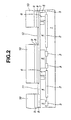
- a masking layer 10 is used and provided in patterning and etching processes to define a plurality of openings through the underlying body including a conductive layer 8 of the first conductivity type as shown in Figure 2.
- the openings are two rectangular openings having different widths, namely, a first opening with a width of X ⁇ m, and a second opening with a width X + ⁇ ⁇ m.
- the masking layer 10 has such first and second openings over the selected regions or desired locations of emitter base junctions 20 (see Figure 7) of the first and second bipolar transistors 31 and 32.
- the openings defined through the underlying body expose the selected regions 11 and 12 of a semiconductor substrate (1, 4, 7), respectively, within bottoms of the openings, exposing sidewalls of the underlying body including the conductive layer 8.
- the selected regions 11 and 12 define emitter base junction areas of the first and second bipolar transistors 31 and 32, respectively, which are configured in the surface region of the semiconductor substrate.
- the semiconductor substrate includes a silicon substrate 1 according to the exemplary embodiment.
- Buried collector regions 2 heavily doped with dopant of a first conductivity type are formed in the substrate surface as shown in Figures 1 to 7.
- the substrate surface region includes so-called guard ring regions 3, each surrounding one of the buried collector regions 2, for isolating the adjacent circuit elements from each other in cooperation with the overlying oxide regions 5.
- the substrate surface region also includes collector electrodes 6 and a layer 4 of epitaxial silicon lightly doped with dopant of the first conductivity type.
- the epitaxial layer 4 overlies the buried collector regions 2 and guard ring regions 3.
- the oxide regions 5 and collector electrodes 6 are buried in the epitaxial layer 4.
- the first and second bipolar transistors 31 and 32 each, have a buried collector region 2 configured in the semiconductor substrate, extrinsic base regions 19 of a second conductivity type configured in the surface region of the semiconductor substrate, and an emitter base junction 20 between an emitter structure 17 and the underlying intrinsic base region.
- Each of the emitter structures 17 includes a layer of an emitter material of the first conductivity type filling the emitter opening in the conductive layer 8 that serves as a collector electrode.
- the emitter material of each of the emitter structure 17 is isolated from the conductive layer 8 by an isolation layer including sidewall spacers (14, 16) and forms an emitter base junction 20 with the underlying intrinsic base region surrounded by extrinsic base regions 16
- the emitter base junctions of the bipolar transistors 31 and 32 have different emitter contact widths.
- the emitter base junction of the first bipolar transistor 31 has a first emitter contact width X ⁇ m
- the emitter base junction of the second bipolar transistor 32 has a second emitter contact width X + ⁇ ⁇ m, which greater or wider than the first emitter contact width.
- the exemplary embodiment describes a structure including a NPN bipolar transistor or PNP bipolar transistor as the first and second bipolar transistors 31 and 32.
- a substrate for an integrated circuit in the form of a semiconductor substrate is provided.
- the semiconductor substrate includes a silicon substrate 1.
- buried collector regions 2, heavily doped with N-type dopant, are configured in the substrate surface.
- the substrate surface region includes a layer 4 of epitaxial silicon lightly doped with N-type dopant. Buried in the epitaxial layer 4 are guard ring regions 3, each surrounding one of the buried collector regions 2, for isolating the adjacent circuit elements from each other in cooperation with the overlying field isolation oxide regions 5, and collector electrodes 6 contacting with the buried collector regions 2.
- the surface of the semiconductor substrate is planarized to expose the epitaxial layer 4, field isolation oxide regions 5 and collector electrodes 6.
- a conductive layer 8, in the form of a polysilicon layer of P conductivity type, is provided over the surface oxide film layer 7.
- a nitride film 9 is deposited over the polysilicon layer 8.
- the masking layer 10 has a first opening with a width of X ⁇ m, and a second opening with a width X + ⁇ ⁇ m over the selected regions 11 and 12 of the semiconductor substrate where emitter base junctions 20 (see Figure 7) are desired to be located.
- the etching, using the masking layer 10 defines openings through the underlying nitride layer 9 and conductive layer 8.
- the surface oxide film layer 7 is removed and an undercut to produce an overhang in the overlying conductive layer 8 (see Figure 3).
- the selected regions 11 and 12 are of the substrate are exposed within the bottoms of the openings and sidewalls of the layers 7, 8 and 9 are exposed.
- a polysilicon material is grown to fill the openings and the undercuts in the surface oxide film layer 7 and selectively removed leaving portions filling the undercuts, forming base contacts 13 between the conductive layer 8 and extrinsic base regions 19 (see Figures 6 and 7). Subsequently, the masking layer 10 is removed.
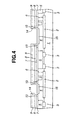
- an oxide film 14 is deposited overall, for example, by growing process. Active base regions 15 are formed below the selected regions 11 and 12 by an appropriate method, such as, ion implantation through the oxide film 14.
- a nitride film 16 is deposited overall, for example, by growing process.
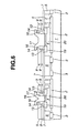
- the nitride film 16 and the underlying oxide film 14 are anisotropically etched back, to leave sidewall spaces (14, 16) on sidewalls of base contacts 13, conductive layer 8 and nitride layer 9. Subsequently, the portions of the oxide film 14 are removed to expose the selected regions 11 and 12 where emitters are to be formed.
- a layer of emitter material in the form of a polysilicon layer 17 is deposited overall to fill the emitter openings defined by the sidewall spacers and etched back using an appropriate masking layer, not shown, to leave portions forming emitter structures 17.
- the layers 8 and 9 are etched leaving base electrodes 8 and the overlying nitride layer 9 portions. Due to heat of the polysilicon layer 17, dopant within the active regions 15 are diffused to form extrinsic base regions 16 and intrinsic base regions.
- Each of the emitter structures 17 in the emitter openings forms an emitter base junction, and it is isolated from the base contacts 13 by the sidewall spacers (14, 16).
- an insulating layer 18 is deposited overall, and conventional metallization steps are provided, including contact 21 formations to the collector base and emitter.
- PNP bipolar transistors could by provided by a complementary process to provide elements of opposite conductivity type, if desired.
Landscapes
- Bipolar Transistors (AREA)
- Semiconductor Integrated Circuits (AREA)
- Bipolar Integrated Circuits (AREA)
Abstract
An integrated circuit comprises a plurality of
bipolar transistors. In an exemplary embodiment, each
bipolar transistor includes a buried collector region
configured in a semiconductor substrate, extrinsic base
regions configured in the surface region of the substrate,
and an emitter base junction. The emitter base junctions
of the bipolar transistors have different emitter
contact widths.
Description
- The present invention relates to integrated circuits, and more particularly relates to integrated circuits including bipolar transistors.
- A continuing trend in fabrication of bipolar transistors for silicon integrated circuits is to build high speed and performance bipolar transistors in integrated circuits. The drive toward this high speed and performance elements in integrated circuits has resulted in continued shrinking of device and circuit features. Such shrinking is intended to shorten carrier travel time by reducing collector base parasitic capacitances, lowering base resistances and accomplishing shallow emitter base junctions.
- The emitter base junction of a bipolar transistor has an emitter contact width.. As is known to one ordinary skill in the art, shrinking emitter contact width would lower electrostatic discharge (ESD) breakdown voltage of the bipolar transistor. The relationship between ESD breakdown voltage and emitter contact width is illustrated in Figure 9. Excessively low ESD breakdown voltage might causes serious damage on the bipolar transistors in an integrated circuit.
- Various measures have been proposed to solve or alleviate this problem. One such measure is to use an ESD protection circuit. Coupling such ESD protection circuit to bipolar transistors in an integrated circuit would alter the device characteristic. Thus, the use of ESD protection circuit is not appropriate where the device characteristic of the integrated circuit should remain unaltered. Other measure is to increase emitter base junction area to avoid the excessive concentration of electric field. If this measure is employed, the chip size will increase considerably, deteriorating high frequency characteristic of bipolar transistor. Thus, this measure is not satisfactory.
- Accordingly, a need remains for development of an integrated circuit with bipolar transistors, which combines high frequency transistor characteristic with sufficiently high ESD breakdown voltage.
- The present invention seeks to provide an integrated circuit and a method of forming bipolar transistors for an integrated circuit, in which the above-mentioned problems are avoided or reduced.
- According to one aspect of the present invention, there is provided an integrated circuit, comprising:
- a semiconductor substrate including a surface region; and
- a plurality of bipolar transistors, each having an emitter base junction in the surface region of the semiconductor substrate,
- the emitter base junctions of the plurality of bipolar transistors having different emitter contact widths.
-
- According to another aspect of the present invention, there is provided a method of forming a plurality of bipolar transistors for an integrated circuit, comprising:
- providing a semiconductor substrate for an integrated circuit;
- providing a conductive layer;
- providing a masking layer over the conductive layer;
- patterning and etching the masking layer to define a plurality of openings therethrough and through the underlying conductive layer exposing a plurality of selected regions of the substrate within bottoms of the plurality of openings and exposing sidewalls of the conductive layer, said selected regions defining emitter base junction areas of the plurality of bipolar transistors, respectively;
- removing the masking layer;
- providing an isolation layer including sidewall spacers on the exposed sidewalls of the conductive layer;
- forming intrinsic base regions within the openings, respectively;
- forming emitter structures within the openings, respectively, each of the emitter structures including a layer of an emitter material filling one of the openings in the conductive layer of the first conductivity type, the emitter material of each of the emitter structures being isolated from the conductive layer by the sidewall spacers and forming an emitter base junction within the underlying intrinsic base region within the one opening,
- the emitter base junctions having different emitter contact widths.
-
- The foregoing and other objects, features and advantages of the invention will be apparent from the following more particular description of exemplary embodiments of the invention as illustrated in the accompanying drawings. The drawings are not necessarily scale, emphasis instead being placed upon illustrating the principles of the invention.
- Figures 1 to 7 are schematic cross sectional views summarizing processes in the fabrication sequences.
- Figure 8 is a fragmentary top plan view a masking layer.
- Figure 9 is a graph illustrating the relationships between ESD breakdown voltage and emitter contact width and between high frequency characteristic and emitter contact width.
- The process steps and structures described below do not form a complete process flow for forming bipolar transistors for an integrated circuit. The present invention can be practiced in conjunction with integrated circuit fabrication techniques currently used in the art, and only so much of the commonly practiced process steps are included as are necessary for an understanding of the present invention. The figures representing cross sections of portions of a device during fabrication are not drawn to scale, but instead are drawn to illustrate the features of the present invention.
- With reference to Figure 7, there is illustrated a portion of an exemplary embodiment of an integrated circuit (IC) according to the present invention. In the embodiment, the IC comprises a plurality of circuit elements including at least one internally connected circuit element in the form of a first
bipolar transistor 31, i.e., a circuit element internally connected to another or other circuit element(s), and at least one externally connected circuit element in the form of a secondbipolar transistor 32, i.e., a circuit element externally connected to another or other device. The exemplary embodiment provides the firstbipolar transistor 31 with high frequency characteristic by narrowing its emitter contact width to reduce base collector capacity, and the secondbipolar transistor 32 with high ESD breakdown voltage by maintaining its emitter contact width. The emitter contact widths of emitter base junctions of thebipolar transistors bipolar transistors masking layer 10 is used and provided in patterning and etching processes to define a plurality of openings through the underlying body including aconductive layer 8 of the first conductivity type as shown in Figure 2. As best seen in Figure 8, the openings are two rectangular openings having different widths, namely, a first opening with a width of X µm, and a second opening with a width X + α µm. Themasking layer 10 has such first and second openings over the selected regions or desired locations of emitter base junctions 20 (see Figure 7) of the first and secondbipolar transistors selected regions conductive layer 8. Theselected regions bipolar transistors - The semiconductor substrate includes a
silicon substrate 1 according to the exemplary embodiment. Buriedcollector regions 2 heavily doped with dopant of a first conductivity type are formed in the substrate surface as shown in Figures 1 to 7. The substrate surface region includes so-calledguard ring regions 3, each surrounding one of the buriedcollector regions 2, for isolating the adjacent circuit elements from each other in cooperation with the overlyingoxide regions 5. The substrate surface region also includescollector electrodes 6 and alayer 4 of epitaxial silicon lightly doped with dopant of the first conductivity type. Theepitaxial layer 4 overlies the buriedcollector regions 2 andguard ring regions 3. Theoxide regions 5 andcollector electrodes 6 are buried in theepitaxial layer 4. - With reference again to Figure 7, the first and second
bipolar transistors collector region 2 configured in the semiconductor substrate,extrinsic base regions 19 of a second conductivity type configured in the surface region of the semiconductor substrate, and anemitter base junction 20 between anemitter structure 17 and the underlying intrinsic base region. Each of theemitter structures 17 includes a layer of an emitter material of the first conductivity type filling the emitter opening in theconductive layer 8 that serves as a collector electrode. The emitter material of each of theemitter structure 17 is isolated from theconductive layer 8 by an isolation layer including sidewall spacers (14, 16) and forms anemitter base junction 20 with the underlying intrinsic base region surrounded byextrinsic base regions 16 - As mentioned before in connection with Figures 2 and 8, according to the exemplary embodiment, the emitter base junctions of the
bipolar transistors bipolar transistor 31 has a first emitter contact width X µm, while the emitter base junction of the secondbipolar transistor 32 has a second emitter contact width X + α µm, which greater or wider than the first emitter contact width. - Clearly, the exemplary embodiment describes a structure including a NPN bipolar transistor or PNP bipolar transistor as the first and second
bipolar transistors - In a method of forming
bipolar transistors silicon substrate 1. As shown in Figure 1, buriedcollector regions 2, heavily doped with N-type dopant, are configured in the substrate surface. The substrate surface region includes alayer 4 of epitaxial silicon lightly doped with N-type dopant. Buried in theepitaxial layer 4 areguard ring regions 3, each surrounding one of the buriedcollector regions 2, for isolating the adjacent circuit elements from each other in cooperation with the overlying fieldisolation oxide regions 5, andcollector electrodes 6 contacting with the buriedcollector regions 2. The surface of the semiconductor substrate is planarized to expose theepitaxial layer 4, fieldisolation oxide regions 5 andcollector electrodes 6. The substrate surface of overlaid by a surfaceoxide film layer 7. Aconductive layer 8, in the form of a polysilicon layer of P conductivity type, is provided over the surfaceoxide film layer 7. Anitride film 9 is deposited over thepolysilicon layer 8. - With reference to Figures 2 and 8, patterning and etching processes using a
masking layer 10 are described. Themasking layer 10 has a first opening with a width of X µm, and a second opening with a width X + α µm over the selectedregions masking layer 10, defines openings through theunderlying nitride layer 9 andconductive layer 8. Then, with another etching using thesame making layer 10, the surfaceoxide film layer 7 is removed and an undercut to produce an overhang in the overlying conductive layer 8 (see Figure 3). As a result, the selectedregions layers - With reference to Figure 3, a polysilicon material is grown to fill the openings and the undercuts in the surface
oxide film layer 7 and selectively removed leaving portions filling the undercuts, formingbase contacts 13 between theconductive layer 8 and extrinsic base regions 19 (see Figures 6 and 7). Subsequently, themasking layer 10 is removed. - With reference to Figure 4, an
oxide film 14 is deposited overall, for example, by growing process.Active base regions 15 are formed below the selectedregions oxide film 14. - Subsequently, a
nitride film 16 is deposited overall, for example, by growing process. - With reference to Figure 5, the
nitride film 16 and theunderlying oxide film 14 are anisotropically etched back, to leave sidewall spaces (14, 16) on sidewalls ofbase contacts 13,conductive layer 8 andnitride layer 9. Subsequently, the portions of theoxide film 14 are removed to expose the selectedregions - With reference to Figure 6, a layer of emitter material in the form of a
polysilicon layer 17, is deposited overall to fill the emitter openings defined by the sidewall spacers and etched back using an appropriate masking layer, not shown, to leave portions formingemitter structures 17. Thelayers base electrodes 8 and theoverlying nitride layer 9 portions. Due to heat of thepolysilicon layer 17, dopant within theactive regions 15 are diffused to formextrinsic base regions 16 and intrinsic base regions. - Each of the
emitter structures 17 in the emitter openings forms an emitter base junction, and it is isolated from thebase contacts 13 by the sidewall spacers (14, 16). - With reference to Figure 7, an insulating
layer 18 is deposited overall, and conventional metallization steps are provided, includingcontact 21 formations to the collector base and emitter. - Clearly, while the embodiment describes a process for formation of NPN bipolar transistors, PNP bipolar transistors could by provided by a complementary process to provide elements of opposite conductivity type, if desired.
- While the present invention has been particularly described, in conjunction with the exemplary embodiments, it is evident that many alternatives, modifications and variations will be apparent to those skilled in the art in light of the foregoing description. It is therefore contemplated that the appended claims will embrace any such alternatives, modifications and variations as falling within the true scope and spirit of the present invention.
Claims (4)
- An integrated circuit, comprising:a semiconductor substrate including a surface region; anda plurality of bipolar transistors, each having a an emitter base junction in the surface region of the semiconductor substrate,the emitter base junctions of the plurality of bipolar transistors having different emitter contact widths.
- An integrated circuit, comprising:a semiconductor substrate including a surface region;an internally connected circuit element in the form of a first bipolar transistor including an emitter base junction, in the surface region of the semiconductor substrate, having a first emitter contact width; andan externally connected circuit element in the form of a second bipolar transistor including an emitter base junction, in the surface region of the semiconductor substrate, having a second emitter contact width,the second emitter contact width being greater than the first emitter contact width.
- A method of forming a plurality of bipolar transistors for an integrated circuit, comprising:providing a semiconductor substrate for an integrated circuit;providing a conductive layer over the substrate;providing a masking layer over the conductive layer;patterning and etching the masking layer to define a plurality of openings therethrough and through the underlying conductive layer exposing a plurality of selected regions of the substrate within bottoms of the plurality of openings and exposing sidewalls of the conductive layer, said selected regions defining emitter base junction areas of the plurality of bipolar transistors, respectively;removing the masking layer;providing an isolation layer including sidewall spacers on the exposed sidewalls of the conductive layer;forming intrinsic base regions within the openings, respectively;forming emitter structures within the openings, respectively, each of the emitter structures including a layer of an emitter material filling one of the openings in the conductive layer, the emitter material of each of the emitter structures being isolated from the conductive layer by the sidewall spacers and forming an emitter base junction within the underlying intrinsic base region within the one opening,the emitter base junctions having different emitter contact widths.
- A method of forming a plurality of bipolar transistors for an integrated circuit, comprising:providing a semiconductor substrate for an integrated circuit;providing a conductive layer over the substrate;providing a masking layer over the conductive layer;patterning and etching the masking layer to define a plurality of openings therethrough and through the underlying conductive layer exposing a plurality of selected regions of the substrate within bottoms of the plurality of openings and exposing sidewalls of the conductive layer, said selected regions defining emitter base junction areas of a first bipolar transistor and a second bipolar, respectively;removing the masking layer;providing an isolation layer including sidewall spacers on the exposed sidewalls of the conductive layer;forming intrinsic base regions within the openings, respectively;forming emitter structures within the openings, respectively, each of the emitter structures including a layer of an emitter material filling one of the openings in the conductive layer, the emitter material of each of the emitter structures being isolated from the conductive layer by the sidewall spacers and forming an emitter base junction within the underlying intrinsic base region within the one opening,the emitter base junction of the first bipolar transistor having a first emitter contact width, the emitter base junction of the second bipolar transistor having a second emitter contact width greater than the first emitter contact width.
Applications Claiming Priority (2)
| Application Number | Priority Date | Filing Date | Title |
|---|---|---|---|
| JP2001026456A JP2002231818A (en) | 2001-02-02 | 2001-02-02 | Semiconductor integrated circuit |
| JP2001026456 | 2001-02-02 |
Publications (1)
| Publication Number | Publication Date |
|---|---|
| EP1229585A1 true EP1229585A1 (en) | 2002-08-07 |
Family
ID=18891270
Family Applications (1)
| Application Number | Title | Priority Date | Filing Date |
|---|---|---|---|
| EP02002474A Withdrawn EP1229585A1 (en) | 2001-02-02 | 2002-02-01 | Integrated circuit with bipolar transistors having different emitter base junction widths |
Country Status (3)
| Country | Link |
|---|---|
| US (1) | US20020105053A1 (en) |
| EP (1) | EP1229585A1 (en) |
| JP (1) | JP2002231818A (en) |
Families Citing this family (3)
| Publication number | Priority date | Publication date | Assignee | Title |
|---|---|---|---|---|
| US8791546B2 (en) * | 2010-10-21 | 2014-07-29 | Freescale Semiconductor, Inc. | Bipolar transistors having emitter-base junctions of varying depths and/or doping concentrations |
| US20160380067A1 (en) | 2015-06-23 | 2016-12-29 | Globalfoundries Inc. | Shaped terminals for a bipolar junction transistor |
| US9761608B1 (en) * | 2016-08-15 | 2017-09-12 | International Business Machines Corporation | Lateral bipolar junction transistor with multiple base lengths |
Citations (4)
| Publication number | Priority date | Publication date | Assignee | Title |
|---|---|---|---|---|
| EP0342695A2 (en) * | 1988-05-20 | 1989-11-23 | Fujitsu Limited | Semiconductor device |
| US5866462A (en) * | 1995-09-29 | 1999-02-02 | Analog Devices, Incorporated | Double-spacer technique for forming a bipolar transistor with a very narrow emitter |
| JPH11307538A (en) * | 1998-04-17 | 1999-11-05 | Sony Corp | Semiconductor device and manufacturing method thereof |
| EP0967642A1 (en) * | 1998-06-26 | 1999-12-29 | Mitel Semiconductor Limited | Semiconductor device including a plurality of bipolar transistors |
-
2001
- 2001-02-02 JP JP2001026456A patent/JP2002231818A/en not_active Withdrawn
-
2002
- 2002-02-01 EP EP02002474A patent/EP1229585A1/en not_active Withdrawn
- 2002-02-01 US US10/061,118 patent/US20020105053A1/en not_active Abandoned
Patent Citations (4)
| Publication number | Priority date | Publication date | Assignee | Title |
|---|---|---|---|---|
| EP0342695A2 (en) * | 1988-05-20 | 1989-11-23 | Fujitsu Limited | Semiconductor device |
| US5866462A (en) * | 1995-09-29 | 1999-02-02 | Analog Devices, Incorporated | Double-spacer technique for forming a bipolar transistor with a very narrow emitter |
| JPH11307538A (en) * | 1998-04-17 | 1999-11-05 | Sony Corp | Semiconductor device and manufacturing method thereof |
| EP0967642A1 (en) * | 1998-06-26 | 1999-12-29 | Mitel Semiconductor Limited | Semiconductor device including a plurality of bipolar transistors |
Non-Patent Citations (1)
| Title |
|---|
| PATENT ABSTRACTS OF JAPAN vol. 2000, no. 02 29 February 2000 (2000-02-29) * |
Also Published As
| Publication number | Publication date |
|---|---|
| US20020105053A1 (en) | 2002-08-08 |
| JP2002231818A (en) | 2002-08-16 |
Similar Documents
| Publication | Publication Date | Title |
|---|---|---|
| JP3130323B2 (en) | MOSFET having substrate source contact and method of manufacturing the same | |
| US5516710A (en) | Method of forming a transistor | |
| US5428243A (en) | Bipolar transistor with a self-aligned heavily doped collector region and base link regions. | |
| KR100603881B1 (en) | Formation process of bipolar transistor having laminated outer base and intermediate semiconductor structure used in the process | |
| KR20000031553A (en) | High speed transistor of bipolar and fabricating method thereof | |
| KR100200485B1 (en) | MOS transistor and manufacturing method thereof | |
| KR100292905B1 (en) | Bipolar transistor on a semiconductor-on-insulator substrate and method for manufacturing thereof | |
| US5591651A (en) | Method of making a bipolar stripe transistor structure | |
| EP0637838A2 (en) | Integrated circuit with self-aligned isolation | |
| EP0951074A2 (en) | Multi-emitter bipolar transistor | |
| CN114628490A (en) | Heterojunction bipolar transistor with undercut extrinsic base region | |
| EP1229585A1 (en) | Integrated circuit with bipolar transistors having different emitter base junction widths | |
| JP2628988B2 (en) | Semiconductor device and manufacturing method thereof | |
| CN119314941A (en) | Deep trench isolation structure and manufacturing method thereof | |
| CA2130806C (en) | Semiconductor device | |
| JPH0897225A (en) | Semiconductor device and manufacturing method thereof | |
| CN118352352A (en) | Electrostatic Devices | |
| EP1228533B1 (en) | Method of manufacturing a bipolar transistor semiconductor device | |
| US12278269B2 (en) | Bipolar transistor with stepped emitter | |
| JPS5915494B2 (en) | Manufacturing method of semiconductor device | |
| KR0137568B1 (en) | Method of making a bipolar transistor | |
| CN119314943A (en) | Deep trench isolation structure and manufacturing method thereof | |
| KR100278424B1 (en) | Thin active layer semiconductor device with high breakdown voltage | |
| US6300220B1 (en) | Process for fabricating isolation structure for IC featuring grown and buried field oxide | |
| KR19980063791A (en) | Well isolated bipolar transistor |
Legal Events
| Date | Code | Title | Description |
|---|---|---|---|
| PUAI | Public reference made under article 153(3) epc to a published international application that has entered the european phase |
Free format text: ORIGINAL CODE: 0009012 |
|
| AK | Designated contracting states |
Kind code of ref document: A1 Designated state(s): AT BE CH CY DE DK ES FI FR GB GR IE IT LI LU MC NL PT SE TR |
|
| AX | Request for extension of the european patent |
Free format text: AL;LT;LV;MK;RO;SI |
|
| 17P | Request for examination filed |
Effective date: 20020620 |
|
| AKX | Designation fees paid |
Designated state(s): DE NL |
|
| RAP1 | Party data changed (applicant data changed or rights of an application transferred) |
Owner name: NEC ELECTRONICS CORPORATION |
|
| STAA | Information on the status of an ep patent application or granted ep patent |
Free format text: STATUS: THE APPLICATION HAS BEEN WITHDRAWN |
|
| 18W | Application withdrawn |
Effective date: 20040204 |